EP1323281B1 - Apparatus and method for enhancing low-frequency operation of mobile communication antennas - Google Patents
Apparatus and method for enhancing low-frequency operation of mobile communication antennas Download PDFInfo
- Publication number
- EP1323281B1 EP1323281B1 EP01958358A EP01958358A EP1323281B1 EP 1323281 B1 EP1323281 B1 EP 1323281B1 EP 01958358 A EP01958358 A EP 01958358A EP 01958358 A EP01958358 A EP 01958358A EP 1323281 B1 EP1323281 B1 EP 1323281B1
- Authority
- EP
- European Patent Office
- Prior art keywords
- pwb
- ground
- enlarger
- antenna
- electrically
- Prior art date
- Legal status (The legal status is an assumption and is not a legal conclusion. Google has not performed a legal analysis and makes no representation as to the accuracy of the status listed.)
- Expired - Lifetime
Links
- 238000010295 mobile communication Methods 0.000 title claims abstract description 28
- 238000000034 method Methods 0.000 title claims description 16
- 230000002708 enhancing effect Effects 0.000 title claims description 8
- 238000004891 communication Methods 0.000 claims abstract description 39
- 238000010276 construction Methods 0.000 description 18
- 230000005855 radiation Effects 0.000 description 9
- 230000001413 cellular effect Effects 0.000 description 2
- 230000005284 excitation Effects 0.000 description 2
- 238000004519 manufacturing process Methods 0.000 description 2
- 239000002184 metal Substances 0.000 description 2
- 238000010521 absorption reaction Methods 0.000 description 1
- 239000004020 conductor Substances 0.000 description 1
- 230000008878 coupling Effects 0.000 description 1
- 238000010168 coupling process Methods 0.000 description 1
- 238000005859 coupling reaction Methods 0.000 description 1
- 238000009826 distribution Methods 0.000 description 1
- 238000005516 engineering process Methods 0.000 description 1
- 238000012986 modification Methods 0.000 description 1
- 230000004048 modification Effects 0.000 description 1
- 239000003973 paint Substances 0.000 description 1
- 238000002360 preparation method Methods 0.000 description 1
- 239000000758 substrate Substances 0.000 description 1
Images


Classifications
-
- H—ELECTRICITY
- H01—ELECTRIC ELEMENTS
- H01Q—ANTENNAS, i.e. RADIO AERIALS
- H01Q1/00—Details of, or arrangements associated with, antennas
- H01Q1/12—Supports; Mounting means
- H01Q1/22—Supports; Mounting means by structural association with other equipment or articles
- H01Q1/24—Supports; Mounting means by structural association with other equipment or articles with receiving set
- H01Q1/241—Supports; Mounting means by structural association with other equipment or articles with receiving set used in mobile communications, e.g. GSM
- H01Q1/242—Supports; Mounting means by structural association with other equipment or articles with receiving set used in mobile communications, e.g. GSM specially adapted for hand-held use
- H01Q1/243—Supports; Mounting means by structural association with other equipment or articles with receiving set used in mobile communications, e.g. GSM specially adapted for hand-held use with built-in antennas
-
- H—ELECTRICITY
- H01—ELECTRIC ELEMENTS
- H01Q—ANTENNAS, i.e. RADIO AERIALS
- H01Q1/00—Details of, or arrangements associated with, antennas
- H01Q1/48—Earthing means; Earth screens; Counterpoises
-
- H—ELECTRICITY
- H01—ELECTRIC ELEMENTS
- H01Q—ANTENNAS, i.e. RADIO AERIALS
- H01Q13/00—Waveguide horns or mouths; Slot antennas; Leaky-waveguide antennas; Equivalent structures causing radiation along the transmission path of a guided wave
- H01Q13/10—Resonant slot antennas
- H01Q13/106—Microstrip slot antennas
-
- H—ELECTRICITY
- H01—ELECTRIC ELEMENTS
- H01Q—ANTENNAS, i.e. RADIO AERIALS
- H01Q9/00—Electrically-short antennas having dimensions not more than twice the operating wavelength and consisting of conductive active radiating elements
- H01Q9/04—Resonant antennas
- H01Q9/0407—Substantially flat resonant element parallel to ground plane, e.g. patch antenna
- H01Q9/0421—Substantially flat resonant element parallel to ground plane, e.g. patch antenna with a shorting wall or a shorting pin at one end of the element
-
- H—ELECTRICITY
- H01—ELECTRIC ELEMENTS
- H01Q—ANTENNAS, i.e. RADIO AERIALS
- H01Q9/00—Electrically-short antennas having dimensions not more than twice the operating wavelength and consisting of conductive active radiating elements
- H01Q9/04—Resonant antennas
- H01Q9/0407—Substantially flat resonant element parallel to ground plane, e.g. patch antenna
- H01Q9/0442—Substantially flat resonant element parallel to ground plane, e.g. patch antenna with particular tuning means
Definitions
- the present invention relates to apparatus, and also to a method, for enhancing the operation of mobile communication antennas particularly in the low-frequency portion of the bandwidth or bandwidths for which the apparatus was designed.
- the invention is particularly useful in mobile communication apparatus (such as mobile telephone handsets) having built-in internal antennas or external antennas, and is therefore described below particularly for such applications.
- Mobile communication equipment including their antennas, are becoming smaller in size as the technology is developed.
- it should usually be about half a wavelength in size, except for monopole-like antennas (which normally operate above a ground plane) where a quarter wavelength is required.
- monopole-like antennas which normally operate above a ground plane
- a quarter wavelength is required.
- advanced mobile communication devices e.g., cellular telephone handsets
- such dimensions are impractical since the overall handset dimensions are smaller than half a wavelength of the appropriate frequency.
- a particular problem in the known internal antennas is their narrow bandwidth of operation.
- the input impedance is unmatched, the radiation efficiency is even further reduced.
- the latter is considered an even more difficult problem in cases where dual-frequency bands, triple-frequency bands, or other multi-band operations of the mobile communication devices are required, such as cellular GSM 900/1800, 900/1900, 900/1800/1900 MHz, etc., or in GPRS (2.5G) and UMTS (3G) applications where bandwidth is the key for operation.
- bandwidth is generally important for all mobile communication applications, in order to maximize the overall system capacity.
- Internal antennas for mobile communication apparatus are known that utilize printed constructions, e.g. patches and slots. These are very convenient to use because of their ease of manufacture, their low profile, and their low production cost. Examples of known internal antenna constructions are described in US Patents 5,262,792 , 5,802,458 , 5,068,670 , 5,929,813 , 5,945,954 , 6,002,367 , and 6,025,802 , and in European Patents 0892459 and 0924797 . If such printed elements could be used in mobile communication devices with respect to efficiency, gain, impedance matching and reproducibility, it would be the best choice. Unfortunately, such elements, because of the small size of the mobile communication device, show very low efficiency and hence low gain; moreover it is difficult to match their impedance to that of the mobile communication device.
- the present invention is particularly directed to mobile communication apparatus which includes a housing containing a printed circuit board, or PCB (now more commonly referred to as a printed wired board or PWB, which term will be hereafter used) carrying the communication circuitry and formed with a signal terminal and an electrically-conductive ground plane for the communication circuitry.
- PCB printed circuit board
- Such apparatus further includes an antenna carried internally within the housing, or externally of the housing, and electrically-connected to the signal terminal, and optionally also to the ground plane of the communication circuitry on the PWB within the housing. While such antennas may be designed in a relatively small and compact form for relatively high radio frequency bands, their operation at low radio frequency bands is relatively inefficient.
- the printed wired board (PWB) carrying the communication circuitry of the mobile communication apparatus actually serves as an extension of the antenna, and enhances its efficiency and bandwidth.
- PWB printed wired board
- mobile communication apparatus comprising: a housing including communication circuitry and a printed wired board (PWB) formed with a signal terminal for an antenna, and an electrically-conductive ground for the communication circuitry; an antenna carried by the housing and electrically connected to the signal terminal of the communication circuitry in the PWB (and optionally to the ground), the antenna being designed to operate in at least one radio frequency band; and an electrically-conductive ground-enlarger carried by the PWB and electrically connected to the electrically-conductive ground of the PWB such that the electrically-mnductive ground-enlarger effectively enlarges the ground of the PWB to load the antenna in said radio frequency band and thereby to enhance the operating efficiency of the antenna particularly in the lower part of said radio frequency band and/or to widen said radio frequency band.
- PWB printed wired board
- the antenna is connected to the signal terminal of the communication circuitry at one end of the PWB, and the electrically-conductive ground-enlarger is connected to the ground of the communication circuitry at the opposite end of the PWB.
- the ground-enlarger may be carried on a separate board from the PWB and electrically connected to the ground of the communication circuitry at the opposite end of the PWB. Since the electrically-conductive ground-enlarger may be added without enlarging the physical size of the PWB, this enhancement of the operation, and/or widening of the bandwidth, of the mobile communication apparatus can be effected without any significant increase In the physical size of the overall apparatus.
- the ground-enlarger includes a pair of stub ground-enlargers formed in the electrically-conductive ground of the PWB at the opposite end of the PWB.
- the opposite end of the PWB includes an electrically-conductive ground on one layer of the PWB, the stub ground-enlargers being defined by slots formed in the electrically-conductive ground on the one layer.
- the stub ground-enlargers may be symmetrical or asymmetrical and may have open or shorted ends, according to the particular application.
- ground of the communication circuitry is carried on one layer of the PWB, and the ground-enlarger is carried on another layer of the PWB.
- the electrically-conductive ground-enlarger is included in a box having a plurality, e.g., six, sides overlying one end of the PWB, at least one of the sides of the box being electrically-conductive and serving as the ground-enlarger electrically connected to the ground of the PWB.
- a method of enhancing the operational efficiency of a mobile communication apparatus in at least one radio frequency band, or to widen its radio frequency band which apparatus comprises a housing including communication circuitry and a printed wired board (PWB) formed with a signal terminal for an antenna and an electrically-conductive ground for the communication circuitry, and an antenna carried by the housing and electrically connected to the signal terminal of the communication circuitry in the PWB; characterized in that the operating efficiency of the antenna is enhanced, particularly in the lower portion of the radio frequency band, or its radio frequency band is widened by connecting an electrically-conductive ground-enlarger to the electrically-conductive ground of the PWB such that the electrically-conductive ground-enlarger effectively enlarges the ground of the PWB to load the antenna in the radio frequency band.
- PWB printed wired board
- the performance enhancement i.e., the antenna gain
- the higher frequency bands e.g., 1800 or 1900 MHz
- the lower bands e.g., 800 or 900 MHz
- the addition of the ground-enlarger or the stub-ground-enlargers may also enhance the bandwidth of all the operation bands in that it also adjusts the antenna operational frequency down to the required lower frequency band.
- the apparatus and method of the present invention are applicable to both internal antennas as well as to external antennas.
- a housing generally designated 2, constituted of a front cover 3 and a back cover 5.
- a printed wired board PWB 4
- PCB printed circuit board
- PWB 4 is formed with a signal terminal indicated at 7, and with an electrically-conductive ground connected to ground terminals 8, 9 for the communication circuitry.
- the ground may be a continuous conductive layer serving as a ground plane, or may be one or more conductive strips serving as a ground for individual components of the communication circuitry.
- terminals 7 - 9 are on the underlying surface of PWB 4 and face an internal antenna, generally designated 10, covering a portion of the PWB 4.
- the internal antenna 10 may be of any desired construction.
- Fig. 2 illustrates one construction, for purposes of example, which is similar to one of those described in our International Patent Application PCT IL/01/00626 filed 9 July 2001 .
- internal antenna 10 includes a PWB constituted of a dielectric substrate having an electrically-conductive layer 13 on one face, serving as the ground plane and cut with a radiant slot 14.
- Slot 14 is of a curved U-shaped configuration, closed at both of its ends, to define two closed side arms 14a, 14b joined by a bridge 14c.
- Radiant slot 14 is excited by an electrically-conductive feed line 15 carried on the opposite face of the dielectric panel and therefore indicated by broken lines in Fig. 2 .
- the antenna illustrated in Fig. 2 is of a symmetrical construction, wherein the two side arms 14a, 14b are substantially parallel and of substantially the same length and width, and are excited by common excitation point, namely the point where the feed line 15 crosses the slot 14.
- the illustrated antenna has a signal input terminal 17 electrically connected to the signal terminal 7 of the PWB 4 ( Fig. 1 ), and two ground terminals 18, 19, electrically connected to the two ground terminals 8, 9 of the PWB 4. These electrical connections may be by pins passing through plated-through-holes (PTHs) or the like.
- the feed line 15 (shown in broken lines in Fig. 2 since it is on the opposite face of the antenna panel 10) includes a main feed line arm 15a connected to the input signal terminal 17. Feed line arm 15a divides the power into two feed line transformer sections 15b, 15c, exciting the slot 14 at two points.
- the transformer sections 15b and 15c continue from the excitation points underneath the slot and perform the function of reactive loads which are shorted to the ground 13, as shown at 16a, 16b. These reactive loads enhance and improve the matching of the slot impedance; that is, they mainly reduce the reactive part of the slot impedance to the order of zero at a broad frequency range.
- the antenna is made resonant and radiant not only at a predetermined high frequency, as determined by the parameters of slot 14, the feed line 15, and the reactive loads, but also at a lower frequency band so as to be capable of use as a multi-band microwave antenna.
- this is done by providing an extension in the form of stub ground-enlargers, or by providing a further panel serving as a continuation of the ground plane 13 at the load side of the slot 14, and thereby effectively enlarging the ground plane to load the antenna in a lower radio frequency band, such as to enhance the operating efficiency of the antenna in the lower radio frequency band.
- a similar technique is used but with respect to the main PWB 4 of the handset 2. This is done by extending the electrically-conductive ground of the printed wired board (PWB) 4 containing the communication circuitry 6, either with an external panel or with stub-ground-enlargers electrically connected to that ground, so as to effectively enlarge that ground. This effectively loads the antenna in the lower radio frequency band, and thereby enhances the operating efficiency of the antenna in the lower radio frequency band and/or widens that band.
- PWB printed wired board
- Fig. 3 illustrates an arrangement wherein the electrically-conductive ground-enlarger, generally designated 30, is attached to the PWB 4 carrying the internal antenna 10.
- the ground-enlarger 30 is in the form of an insulating panel carrying an electrical-conductive layer 31 on one face. It is electrically connected by a terminal 32 to a terminal 33 on the PWB 4 at the end of the PWB opposite to that carrying the internal antenna 10 and the signal terminal 7 of the PWB connected to the signal terminal 17 of the internal antenna.
- the connection between terminals 32 and 33 may be by pin 34 ( Figs. 3b, 3c ); and the connections between the terminals 7 - 9 of the PWB 4 and terminals 17 - 19 of the internal antenna 10 may be by pins 35.
- Fig. 3a illustrates the initial stage in the preparation of the ground-enlarger 30;
- Fig. 3b illustrates the application of the ground-enlarger to underlie the respective end of the PWB 4; and
- Fig. 3c illustrates the application of the ground-enlarger to overlie the respective end of the PWB 4.
- the ground-enlarger 30 acts as a load to the antenna in the lower operational band, by enlarging the ground plane of the main PWB 4 (and thereby of the antenna 10). As described above, this improving antenna matching and enhances the operating efficiency of the antenna in the lower radio frequency band.
- the dimensions and shape of the ground-enlarger 30, as well as the distance from the PWB 4, may vary. Although the ground-enlarger is shown in Figs. 3b and 3c as parallel to the main PWB 4, it may be mounted to the latter at any desired angle.
- the ground-enlarger may be made in any suitable manner, such as by providing a conductive layer on an insulating board, by using a metal plate, metallic paint, metal plated plastic, etc. It may also be an independent part of the apparatus, such as a part of the battery, the housing cover, the keyboard, etc.
- the antenna 10 may also be connected to the ground of the PWB 4, in addition to its connection to the signal terminal 17 of the PWB 4.
- Fig. 4 illustrates a ground-enlarger, generally designated 40, constructed as a flexible part of the PWB 4, or of the conductive layer of that board, at the opposite end carrying the internal antenna 10 and the input signal terminals 7 of the PWB 4, and the corresponding terminal 17 of the internal antenna.
- the ground-enlarger 40 illustrated in Fig. 4 thus also includes an electrically-conductive layer 41 which is connected by a flexible strip 42 to the elecraically-conducfive layer of the PWB 4.
- the ground-enlarger 40 is bent under the respective end of the PWB 4 ( Fig. 4b ), or over the respective end of the PWB 4 ( Fig.
- the antenna 10 is connected to the PWB 4 in any suitable manner, such as by pins 45 passing through the signal terminal 17 and ground terminals 18, 19 in the antenna, and the corresponding terminals 7-9 ( Fig. 1 ) in the PWB 4.
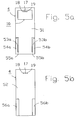
- Fgs. 5a and 5b illustrate a construction wherein the electrically-conductive ground-enlarger is in the form of stub ground-enlargers formed in the end of the PWB 4 opposite to that carrying the internal antenna 10 and the signal input terminal 17 of the antenna.
- the PWB 4 is provided with an electrically-conductive layer on both of its opposite faces, as shown at 51 in Fig. 5a and 52 in Fig. 5b .
- the face 51, shown in Fig. 5a which carries the internal antenna 10, is formed, at the opposite end from that carrying the internal antenna 10, with a pair of slots 53a, 53b, cut in the conductive layer 51 defining the ground plane.
- Each of the slots 53a, 53b is closed at one end and open at the opposite end to define two stub ground-enlargers 54a, 54b, and electrical connections 55a, 55b at the ground plane 51.
- the electrically-conductive layer 52 on the opposite face of the PWB 4 (as shown in Fig. 5b ) is formed with two interruptions 56a, 56b i.e., areas without conductors, in the ground plane 52 in alignment with the stub ground-enlargers 54a, 54b.
- the stub ground-enlargers 54a, 54b thus act similarly to the ground-enlarger 30 in Fig. 3 , to effectively enlarge the ground plane 51 of the PWB 4, but better enable tuning to enhance the operating efficiency of the antenna in the lower radio frequency band.
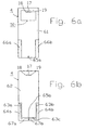
- Figs. 6a and 6b illustrate a construction similar to that of Figs. 5a and 5b , except that the stub ground-enlargers and the interruptions are reversed with respect to the opposite faces of the PWB 4.
- the etectrically-conductive layer 61 on the side of PWB 4 carrying the internal antenna 10 is formed with the interruptions 66a, 66b; whereas the opposite face of the PWB 4 carrying the electrically-conductive layer 62 is formed with the slots 63a, 63b, defining the stub ground-enlargers 64a, 64b.
- the electrical connections for exciting the stub ground-enlargers 64a, 64b are in the form of PTHs 65a, 65b, and the conductive portions 67a, 67b of layer 62 electrically connecting conductive layer 61 to the stub ground-enlargers 64a, 64b; while the slots 63a, 63b insulate the stub ground-enlargers from the electrically-conductive layer 62.
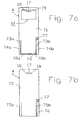
- Figs. 7a and 7b illustrate an arrangement also similar to that of Figs. 5a and 5b , respectively, but wherein the two stub ground-enlargers are of an asymmetrical construction.
- the slots 73a, 73b are cut in the electrically-conductive layer 71 of the PWB 4 in the form of two half-closed slots of different configurations so as to define two stub ground-enlargers 74a, 74b of different configurations and electrically connected to the electrically-conductive layer 71 (serving as the ground) by electrical connections 78a, 78b also of different configurations.
- Interruption 75a in the electrically-conductive layer 72 on the opposite face of the PWB 4 is of a rectangular configuration, whereas interruption 75b is of an L-shaped configuration such as to define a ground-enlarger extension 76 on face 72 ( Fig. 7b ).
- Ground-enlarger extension 76 is electrically connected by a plated-through-hole 77 (or pin, etc) to the stub ground-enlarger 74b on the opposite face of the PWB 4.
- the electrical connections 78a, 78b to the stub ground-enlargers are separated by gap 79 in the two slots 73a, 73b.
- the main PWB 4 can be separately tuned to enhance the antenna operation in two low frequency bands.
- stub ground-enlarger 74a and the ground-enlarger extension 76 shown are open ended, it is appreciated that each of them can also be grounded at its end.
- Figs. 8a and 8b illustrate a construction similar to that of Figs. 6a and 6b , except that the stub ground-enlargers are asymmetrical, and the connections of the antenna 10 to the PWB 4 are by means of two terminals rather than three terminals.
- the internal antenna 10 carried by the PWB 4 includes a signal input terminal 17, but only a ground terminal 18 on one side of the latter terminal. The location of the terminal 18 can be changed as desired.
- interruptions 86a, 86b formed in the conductive layer 81 on one side of the PWB 4, and the slots 83a, 83b, formed in the electrically-conductive layer 82 on the opposite face of the PWB are the same as the corresponding interruptions 66a, 66b and slots 63a, 63b in Figs. 6a, 6b , except that they are asymmetrical.
- the electrical connections for exciting the stub ground-enlargers 84a, 84b in the form of PTH 85a, 85b or the like, the electrical connections 87a, 87b electrically connecting conductive layer 81 to the stub ground-enlargers are asymmetrical as well.
- stub ground-enlargers could be used.
- the stub ground-enlargers could include, discrete reactive elements, such as described in U.S. Patent 5,068,670 .
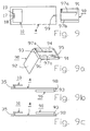
- Fig. 9 illustrates a construction wherein the electrically-conductive ground-enlarger, therein designated 90, is in the form of a plural-sided, i.e., six-sided box to be carried by the end of the PWB 4 opposite to that carrying the internal antenna 10 and the signal input terminal 17 of that ground-enlarger.
- the six sides of box ground-enlarger 90 are shown at 91 - 96, respectively, in Fig. 9a .
- Side 91 includes an electrically-conductive layer formed with an open slot 97a, and a closed slot 97b.
- Side 93 is made completely electrically-conductive, whereas the remaining sides 92, 94, 95 and 96 are electrically insulating.
- the ground-enlarger box 90 may be mounted below the PWB 4 ( Fig. 9b ) or above ( Fig. 9c ). In either case, its electrically-conductive layers (91, 93) are electrically connected to the electrically-conductive layer of the PWB 4 in any suitable manner, e.g., as by a spring-loaded conductive pin 98 passing through a plated-through-hole 99 in the PWB 4 and engaging electrically-conductive side 93.
- the purpose of the electrically-conductive layers of the ground-enlarger 90 is to effectively enlarge the ground plane of the PWB 4 so as to load the antenna 10 in the lower radio frequency band, and thereby to enhance the operating efficiency of the antenna in the lower radio frequency band.
- the ground-enlarger box 90 may therefore have a different number or arrangement of electrically-conductive layers for effectively enlarging the ground of the PWB 4.
- the slots 97a, 97b may be of different locations and/or configurations to improve the matching, and thereby to enhance the radiation of the antenna in the desired operational band. In some cases, only one slot, or no slots, may be provided.
- the antenna is an internal antenna. It will be appreciated, however, that the invention could also be implemented in mobile communication apparatus having external antennas.
- the electrically-conductive ground-enlarger, shown at 105, for effectively enlarging the ground of the PWB 103 to load the antenna 104 in a lower radio frequency band may be any of the constructions described above. It is electrically connected to the ground conductive layer 106 at the opposite end of the PWB 103 connected to the antenna by a pin 107 passing through PTHs 108, 109 in the PWB and the ground-enlarger, respectively.
- the ground-enlarger 105 may be mounted to underlie the PWB 103 as shown in Fig. 10b , to overlie it as shown in Fig. 10c , or at any angle thereto.
- Figs. 11a and 11b illustrate another implementation of the invention, in the form of a mobile telephone handset, generally designated 110, including a main housing 112 containing the main PWB 113, an external antenna 114, and a flip section 115 containing the microphone of the handset.
- the ground-enlarger provided to effectively enlarge the ground of the PWB 113 is carried by the flip section 115 as shown at 116.
- the ground-enlarger 116 is electrically connected to the ground of the PWB 113 at its end opposite to that connected to the external antenna 114 in any suitable manner, e.g., by an electrically-conductive flexible 117 in the pivoted coupling of the flip section 115 to the housing 112.
- the housing has two sections movable relative to each other, (e.g., relatively slidable sections), in which the PWB, communication circuitry and signal terminal are in one section.
- the invention may also be implemented in those constructions, e.g., by including the electrically-conductive ground-enlarger in the other section.
Abstract
Description
- The present invention relates to apparatus, and also to a method, for enhancing the operation of mobile communication antennas particularly in the low-frequency portion of the bandwidth or bandwidths for which the apparatus was designed. The invention is particularly useful in mobile communication apparatus (such as mobile telephone handsets) having built-in internal antennas or external antennas, and is therefore described below particularly for such applications.
- Mobile communication equipment, including their antennas, are becoming smaller in size as the technology is developed. For an antenna to operate properly, it should usually be about half a wavelength in size, except for monopole-like antennas (which normally operate above a ground plane) where a quarter wavelength is required. For advanced mobile communication devices, e.g., cellular telephone handsets, such dimensions are impractical since the overall handset dimensions are smaller than half a wavelength of the appropriate frequency.
- Using small antennas therefore reduces their efficiency, and accordingly requires higher power to be supplied. Higher power reduces the intervals between battery recharges, and increases the radiation into the user's head/body. The level of power radiated into the human head is particularly significant, and serious limitations and specifications are prescribed in order to reduce this possible hazard to the users.
- Operation of such devices in the vicinity of a human body also changes the field and/or current distribution along the antenna, and hence changes its radiation pattern, as well as the radiation efficiency. Practically speaking, the reduction in efficiency may be in the range of 10 - 20 dB or more. External whip antennas, such as the "STUBBY" or retractable antennas, are commonly used to increase the antenna efficiency. However, the use of such antennas is also inconvenient as the antennas are often "caught up" inside the pocket. They also detract from the aesthetic appearance of the mobile communication device. Moreover, their radiation pattern is quasi-omni so as to provide little protection of the user's head/body against excessive radiation.
- Internal antennas supplied by several companies are relatively inefficient as compared to external antennas. Furthermore, these known internal antennas generally do not decrease the radiation into the user's head/body, and in many cases even increase such radiation. The antenna gain is also generally poor (especially while used adjacent to the head/body), and the SAR (Specific Absorption Ratio) results are generally high.
- A particular problem in the known internal antennas is their narrow bandwidth of operation. In addition, where the input impedance is unmatched, the radiation efficiency is even further reduced. The latter is considered an even more difficult problem in cases where dual-frequency bands, triple-frequency bands, or other multi-band operations of the mobile communication devices are required, such as cellular GSM 900/1800, 900/1900, 900/1800/1900 MHz, etc., or in GPRS (2.5G) and UMTS (3G) applications where bandwidth is the key for operation. Further, bandwidth is generally important for all mobile communication applications, in order to maximize the overall system capacity.
- Internal antennas for mobile communication apparatus are known that utilize printed constructions, e.g. patches and slots. These are very convenient to use because of their ease of manufacture, their low profile, and their low production cost. Examples of known internal antenna constructions are described in
US Patents 5,262,792 ,5,802,458 ,5,068,670 ,5,929,813 ,5,945,954 ,6,002,367 , and6,025,802 , and in European Patents0892459 and0924797 . If such printed elements could be used in mobile communication devices with respect to efficiency, gain, impedance matching and reproducibility, it would be the best choice. Unfortunately, such elements, because of the small size of the mobile communication device, show very low efficiency and hence low gain; moreover it is difficult to match their impedance to that of the mobile communication device. - The present invention is particularly directed to mobile communication apparatus which includes a housing containing a printed circuit board, or PCB (now more commonly referred to as a printed wired board or PWB, which term will be hereafter used) carrying the communication circuitry and formed with a signal terminal and an electrically-conductive ground plane for the communication circuitry. Such apparatus further includes an antenna carried internally within the housing, or externally of the housing, and electrically-connected to the signal terminal, and optionally also to the ground plane of the communication circuitry on the PWB within the housing. While such antennas may be designed in a relatively small and compact form for relatively high radio frequency bands, their operation at low radio frequency bands is relatively inefficient. Where the antenna is very small, the printed wired board (PWB) carrying the communication circuitry of the mobile communication apparatus actually serves as an extension of the antenna, and enhances its efficiency and bandwidth. However, since mobile communication devices are becoming smaller in size, this contribution of the PWB to the antenna performance is limited. This limitation applies to all kinds of antennas used with such mobile communication apparatus, i.e., internal antennas as well as external antennas.
- An object of the present invention is to provide mobile communication apparatus including small, compact antennas, wherein the operating efficiency and bandwidth of the antenna are enhanced. Another object of the invention is to provide a method of enhancing the operating efficiency of such antennas.
- The invention is defined in the appended claims.
- According to one aspect there is provided mobile communication apparatus, comprising: a housing including communication circuitry and a printed wired board (PWB) formed with a signal terminal for an antenna, and an electrically-conductive ground for the communication circuitry; an antenna carried by the housing and electrically connected to the signal terminal of the communication circuitry in the PWB (and optionally to the ground), the antenna being designed to operate in at least one radio frequency band; and an electrically-conductive ground-enlarger carried by the PWB and electrically connected to the electrically-conductive ground of the PWB such that the electrically-mnductive ground-enlarger effectively enlarges the ground of the PWB to load the antenna in said radio frequency band and thereby to enhance the operating efficiency of the antenna particularly in the lower part of said radio frequency band and/or to widen said radio frequency band.
- Many embodiments of the invention are described below for purposes of example.
- According to further features in the described preferred embodiments, the antenna is connected to the signal terminal of the communication circuitry at one end of the PWB, and the electrically-conductive ground-enlarger is connected to the ground of the communication circuitry at the opposite end of the PWB. The ground-enlarger may be carried on a separate board from the PWB and electrically connected to the ground of the communication circuitry at the opposite end of the PWB. Since the electrically-conductive ground-enlarger may be added without enlarging the physical size of the PWB, this enhancement of the operation, and/or widening of the bandwidth, of the mobile communication apparatus can be effected without any significant increase In the physical size of the overall apparatus.
- According to further features In some of the described preferred embodiments, the ground-enlarger includes a pair of stub ground-enlargers formed in the electrically-conductive ground of the PWB at the opposite end of the PWB. In some described preferred embodiments, the opposite end of the PWB includes an electrically-conductive ground on one layer of the PWB, the stub ground-enlargers being defined by slots formed in the electrically-conductive ground on the one layer. The stub ground-enlargers may be symmetrical or asymmetrical and may have open or shorted ends, according to the particular application.
- A further embodiment is described wherein the ground of the communication circuitry is carried on one layer of the PWB, and the ground-enlarger is carried on another layer of the PWB.
- According to another preferred embodiment described below, the electrically-conductive ground-enlarger is included in a box having a plurality, e.g., six, sides overlying one end of the PWB, at least one of the sides of the box being electrically-conductive and serving as the ground-enlarger electrically connected to the ground of the PWB.
- According to another aspect, there is provided a method of enhancing the operational efficiency of a mobile communication apparatus in at least one radio frequency band, or to widen its radio frequency band, which apparatus comprises a housing including communication circuitry and a printed wired board (PWB) formed with a signal terminal for an antenna and an electrically-conductive ground for the communication circuitry, and an antenna carried by the housing and electrically connected to the signal terminal of the communication circuitry in the PWB; characterized in that the operating efficiency of the antenna is enhanced, particularly in the lower portion of the radio frequency band, or its radio frequency band is widened by connecting an electrically-conductive ground-enlarger to the electrically-conductive ground of the PWB such that the electrically-conductive ground-enlarger effectively enlarges the ground of the PWB to load the antenna in the radio frequency band.
- In case of two or more operational frequency bands, the performance enhancement (i.e., the antenna gain) would practically be applied to the lower band. That is, the higher frequency bands (e.g., 1800 or 1900 MHz) do not always need this extension for normal operation, and only the lower bands (e.g., 800 or 900 MHz) will be enhanced. However, the addition of the ground-enlarger or the stub-ground-enlargers may also enhance the bandwidth of all the operation bands in that it also adjusts the antenna operational frequency down to the required lower frequency band.
- As indicated earlier, the apparatus and method of the present invention are applicable to both internal antennas as well as to external antennas.
- Further features and advantages of the invention will be apparent from the description below.
- The invention is herein described, by way of example only, with reference to the accompanying drawings, wherein:
-
Fig. 1 is an exploded view illustrating one form of mobile communication apparatus constructed in accordance with the present invention; -
Fig. 2 illustrates an example of an internal antenna which may be used in the apparatus ofFig. 1 ; -
Fig. 3 illustrates one arrangement in accordance with the present invention for enhancing the operating efficiency of the antenna in the apparatus ofFigs. 1 and 2 in the lower radio frequency band,Figs. 3a, 3b and 3c being side views illustrating possible locations of the ground-enlarger; -
Figs. 4, 4a, 4b and 4c are views, corresponding to those ofFigs. 3, 3a, 3b and 3c , respectively, Illustrating another arrangement in accordance with the present invention for enhancing the operating efficiency of the antenna in the lower radio frequency band; -
Figs. 5a and 5b are views of the opposite faces of the PWB in the apparatus ofFigs. 1 and 2 illustrating a further arrangement in accordance with the present invention for enhancing the operating efficiency of the antenna in the lower radio frequency band; -
Figs. 6a, 6b ,7a, 7b and8a, 8b are views corresponding to those ofFigs. 5a and 5b , respectively, illustrating three other arrangements that may be used in accordance with the present invention; -
Fig. 9 illustrates a still further arrangement wherein the electrically-conductive ground-enlarger is in the form of a box having one or more electrically-conductive faces,Fig. 9a illustrating one example of such a box construction, andFigs. 9b and 9c illustrating alternative dispositions of the box with respect to the PWB; -
Figs. 10, 10a, 10b, and 10c are views, corresponding to those ofFigs. 3, 3a, 3b and 3c , respectively, illustrating an arrangement similar to that ofFig. 3 but wherein the antenna is an external antenna, rather than an internal antenna; and -
Figs. 11a and 11b illustrate the invention implemented in a mobile telephone handset having an external antenna,Fig. 11a illustrating the closed position of the handset andFig. 11b illustrating the open position of the handset. - With reference first to
Fig. 1 , there is illustrated one form of mobile communication apparatus constructed in accordance with the present invention, including a housing, generally designated 2, constituted of afront cover 3 and aback cover 5. Withinhousing 2 is a printed wired board (PWB) 4, sometimes referred to as a printed circuit board (PCB), which includes all or a part of the communication circuitry, generally designated 6, of the apparatus.PWB 4 is formed with a signal terminal indicated at 7, and with an electrically-conductive ground connected toground terminals 8, 9 for the communication circuitry. The ground may be a continuous conductive layer serving as a ground plane, or may be one or more conductive strips serving as a ground for individual components of the communication circuitry. - In the apparatus illustrated in
Fig. 1 , terminals 7 - 9 are on the underlying surface ofPWB 4 and face an internal antenna, generally designated 10, covering a portion of thePWB 4. Theinternal antenna 10 may be of any desired construction.Fig. 2 illustrates one construction, for purposes of example, which is similar to one of those described in our International Patent ApplicationPCT IL/01/00626 filed 9 July 2001 - Thus, as more particularly shown in
Fig. 2 ,internal antenna 10 includes a PWB constituted of a dielectric substrate having an electrically-conductive layer 13 on one face, serving as the ground plane and cut with aradiant slot 14.Slot 14 is of a curved U-shaped configuration, closed at both of its ends, to define twoclosed side arms bridge 14c.Radiant slot 14 is excited by an electrically-conductive feed line 15 carried on the opposite face of the dielectric panel and therefore indicated by broken lines inFig. 2 . - The antenna illustrated in
Fig. 2 is of a symmetrical construction, wherein the twoside arms slot 14. - The illustrated antenna has a
signal input terminal 17 electrically connected to thesignal terminal 7 of the PWB 4 (Fig. 1 ), and twoground terminals ground terminals 8, 9 of thePWB 4. These electrical connections may be by pins passing through plated-through-holes (PTHs) or the like. The feed line 15 (shown in broken lines inFig. 2 since it is on the opposite face of the antenna panel 10) includes a mainfeed line arm 15a connected to theinput signal terminal 17.Feed line arm 15a divides the power into two feed line transformer sections 15b, 15c, exciting theslot 14 at two points. The transformer sections 15b and 15c continue from the excitation points underneath the slot and perform the function of reactive loads which are shorted to theground 13, as shown at 16a, 16b. These reactive loads enhance and improve the matching of the slot impedance; that is, they mainly reduce the reactive part of the slot impedance to the order of zero at a broad frequency range. - Further features of the construction and operation of the
internal antenna 10 illustrated inFigs. 1 and 2 , as well as alternative constructions that may be used, are described in the above-cited PCT ApplicationPCT/L01/00626, filed 9 July 2001 - In the above-cited PCT Application, the antenna is made resonant and radiant not only at a predetermined high frequency, as determined by the parameters of
slot 14, the feed line 15, and the reactive loads, but also at a lower frequency band so as to be capable of use as a multi-band microwave antenna. In the above-cited PCT Application, this is done by providing an extension in the form of stub ground-enlargers, or by providing a further panel serving as a continuation of theground plane 13 at the load side of theslot 14, and thereby effectively enlarging the ground plane to load the antenna in a lower radio frequency band, such as to enhance the operating efficiency of the antenna in the lower radio frequency band. - In the present application, a similar technique is used but with respect to the
main PWB 4 of thehandset 2. This is done by extending the electrically-conductive ground of the printed wired board (PWB) 4 containing the communication circuitry 6, either with an external panel or with stub-ground-enlargers electrically connected to that ground, so as to effectively enlarge that ground. This effectively loads the antenna in the lower radio frequency band, and thereby enhances the operating efficiency of the antenna in the lower radio frequency band and/or widens that band. -
Fig. 3 illustrates an arrangement wherein the electrically-conductive ground-enlarger, generally designated 30, is attached to thePWB 4 carrying theinternal antenna 10. The ground-enlarger 30 is in the form of an insulating panel carrying an electrical-conductive layer 31 on one face. It is electrically connected by a terminal 32 to a terminal 33 on thePWB 4 at the end of the PWB opposite to that carrying theinternal antenna 10 and thesignal terminal 7 of the PWB connected to thesignal terminal 17 of the internal antenna. The connection betweenterminals Figs. 3b, 3c ); and the connections between the terminals 7 - 9 of thePWB 4 and terminals 17 - 19 of theinternal antenna 10 may be by pins 35. -
Fig. 3a illustrates the initial stage in the preparation of the ground-enlarger 30;Fig. 3b illustrates the application of the ground-enlarger to underlie the respective end of thePWB 4; andFig. 3c illustrates the application of the ground-enlarger to overlie the respective end of thePWB 4. - It will thus be seen that the ground-
enlarger 30 acts as a load to the antenna in the lower operational band, by enlarging the ground plane of the main PWB 4 (and thereby of the antenna 10). As described above, this improving antenna matching and enhances the operating efficiency of the antenna in the lower radio frequency band. The dimensions and shape of the ground-enlarger 30, as well as the distance from thePWB 4, may vary. Although the ground-enlarger is shown inFigs. 3b and 3c as parallel to themain PWB 4, it may be mounted to the latter at any desired angle. The ground-enlarger may be made in any suitable manner, such as by providing a conductive layer on an insulating board, by using a metal plate, metallic paint, metal plated plastic, etc. It may also be an independent part of the apparatus, such as a part of the battery, the housing cover, the keyboard, etc. - It will also be appreciated that the
antenna 10 may also be connected to the ground of thePWB 4, in addition to its connection to thesignal terminal 17 of thePWB 4. -
Fig. 4 illustrates a ground-enlarger, generally designated 40, constructed as a flexible part of thePWB 4, or of the conductive layer of that board, at the opposite end carrying theinternal antenna 10 and theinput signal terminals 7 of thePWB 4, and the correspondingterminal 17 of the internal antenna. The ground-enlarger 40 illustrated inFig. 4 thus also includes an electrically-conductive layer 41 which is connected by aflexible strip 42 to the elecraically-conducfive layer of thePWB 4. Preferably, the ground-enlarger 40 is bent under the respective end of the PWB 4 (Fig. 4b ), or over the respective end of the PWB 4 (Fig. 4c ) or at any angle thereto, to provide a compact arrangement for thePWB 4 which enhances the operating efficiency of the antenna in the lower radio frequency band, as described above. Theantenna 10 is connected to thePWB 4 in any suitable manner, such as bypins 45 passing through thesignal terminal 17 andground terminals Fig. 1 ) in thePWB 4. - Fgs. 5a and 5b illustrate a construction wherein the electrically-conductive ground-enlarger is in the form of stub ground-enlargers formed in the end of the
PWB 4 opposite to that carrying theinternal antenna 10 and thesignal input terminal 17 of the antenna. In this case, thePWB 4 is provided with an electrically-conductive layer on both of its opposite faces, as shown at 51 inFig. 5a and 52 inFig. 5b . Theface 51, shown inFig. 5a , which carries theinternal antenna 10, is formed, at the opposite end from that carrying theinternal antenna 10, with a pair ofslots conductive layer 51 defining the ground plane. Each of theslots enlargers electrical connections ground plane 51. The electrically-conductive layer 52 on the opposite face of the PWB 4 (as shown inFig. 5b ) is formed with twointerruptions ground plane 52 in alignment with the stub ground-enlargers - The stub ground-
enlargers enlarger 30 inFig. 3 , to effectively enlarge theground plane 51 of thePWB 4, but better enable tuning to enhance the operating efficiency of the antenna in the lower radio frequency band. -
Figs. 6a and 6b illustrate a construction similar to that ofFigs. 5a and 5b , except that the stub ground-enlargers and the interruptions are reversed with respect to the opposite faces of thePWB 4. Thus, as shown inFig. 6a , the etectrically-conductive layer 61 on the side ofPWB 4 carrying theinternal antenna 10 is formed with the interruptions 66a, 66b; whereas the opposite face of thePWB 4 carrying the electrically-conductive layer 62 is formed with theslots enlargers enlargers PTHs conductive portions layer 62 electrically connectingconductive layer 61 to the stub ground-enlargers slots conductive layer 62. -
Figs. 7a and 7b illustrate an arrangement also similar to that ofFigs. 5a and 5b , respectively, but wherein the two stub ground-enlargers are of an asymmetrical construction. Thus, as shown inFig. 7a , theslots conductive layer 71 of thePWB 4 in the form of two half-closed slots of different configurations so as to define two stub ground-enlargers 74a, 74b of different configurations and electrically connected to the electrically-conductive layer 71 (serving as the ground) byelectrical connections Interruption 75a in the electrically-conductive layer 72 on the opposite face of thePWB 4 is of a rectangular configuration, whereasinterruption 75b is of an L-shaped configuration such as to define a ground-enlarger extension 76 on face 72 (Fig. 7b ). Ground-enlarger extension 76 is electrically connected by a plated-through-hole 77 (or pin, etc) to the stub ground-enlarger 74b on the opposite face of thePWB 4. Theelectrical connections gap 79 in the twoslots - By controlling the location, width and length of the
gap 79, and the width and length of each stub ground-enlarger 74a, 74b, each halfopen slot electrical connection ground interruption 75a, the ground-enlarger extension 76 and theslot 75b, themain PWB 4 can be separately tuned to enhance the antenna operation in two low frequency bands. - While the stub ground-enlarger 74a and the ground-
enlarger extension 76 shown are open ended, it is appreciated that each of them can also be grounded at its end. -
Figs. 8a and 8b illustrate a construction similar to that ofFigs. 6a and 6b , except that the stub ground-enlargers are asymmetrical, and the connections of theantenna 10 to thePWB 4 are by means of two terminals rather than three terminals. Thus, theinternal antenna 10 carried by thePWB 4 includes asignal input terminal 17, but only aground terminal 18 on one side of the latter terminal. The location of the terminal 18 can be changed as desired. In addition, theinterruptions 86a, 86b formed in theconductive layer 81 on one side of thePWB 4, and theslots conductive layer 82 on the opposite face of the PWB are the same as the corresponding interruptions 66a, 66b andslots Figs. 6a, 6b , except that they are asymmetrical. The electrical connections for exciting the stub ground-enlargers PTH electrical connections conductive layer 81 to the stub ground-enlargers are asymmetrical as well. - Other constructions for stub ground-enlargers could be used. For example, the stub ground-enlargers could include, discrete reactive elements, such as described in
U.S. Patent 5,068,670 . -
Fig. 9 illustrates a construction wherein the electrically-conductive ground-enlarger, therein designated 90, is in the form of a plural-sided, i.e., six-sided box to be carried by the end of thePWB 4 opposite to that carrying theinternal antenna 10 and thesignal input terminal 17 of that ground-enlarger. The six sides of box ground-enlarger 90 are shown at 91 - 96, respectively, inFig. 9a .Side 91 includes an electrically-conductive layer formed with anopen slot 97a, and aclosed slot 97b.Side 93 is made completely electrically-conductive, whereas the remainingsides - The ground-
enlarger box 90 may be mounted below the PWB 4 (Fig. 9b ) or above (Fig. 9c ). In either case, its electrically-conductive layers (91, 93) are electrically connected to the electrically-conductive layer of thePWB 4 in any suitable manner, e.g., as by a spring-loadedconductive pin 98 passing through a plated-through-hole 99 in thePWB 4 and engaging electrically-conductive side 93. - As described above, the purpose of the electrically-conductive layers of the ground-
enlarger 90 is to effectively enlarge the ground plane of thePWB 4 so as to load theantenna 10 in the lower radio frequency band, and thereby to enhance the operating efficiency of the antenna in the lower radio frequency band. The ground-enlarger box 90 may therefore have a different number or arrangement of electrically-conductive layers for effectively enlarging the ground of thePWB 4. Similarly, theslots - In all the above-described embodiments of the invention, the antenna is an internal antenna. It will be appreciated, however, that the invention could also be implemented in mobile communication apparatus having external antennas.
- One such construction is illustrated in
Fig. 10 , wherein the housing is shown at 102, the PWB containing the communication circuitry of the apparatus is shown at 103, and the external antenna is shown at 104. The electrically-conductive ground-enlarger, shown at 105, for effectively enlarging the ground of thePWB 103 to load theantenna 104 in a lower radio frequency band may be any of the constructions described above. It is electrically connected to the groundconductive layer 106 at the opposite end of thePWB 103 connected to the antenna by apin 107 passing throughPTHs enlarger 105 may be mounted to underlie thePWB 103 as shown inFig. 10b , to overlie it as shown inFig. 10c , or at any angle thereto. -
Figs. 11a and 11b illustrate another implementation of the invention, in the form of a mobile telephone handset, generally designated 110, including amain housing 112 containing themain PWB 113, anexternal antenna 114, and aflip section 115 containing the microphone of the handset. In this embodiment of the invention, the ground-enlarger provided to effectively enlarge the ground of thePWB 113 is carried by theflip section 115 as shown at 116. The ground-enlarger 116 is electrically connected to the ground of thePWB 113 at its end opposite to that connected to theexternal antenna 114 in any suitable manner, e.g., by an electrically-conductive flexible 117 in the pivoted coupling of theflip section 115 to thehousing 112. - Other constructions of mobile telephone handsets are known in which the housing has two sections movable relative to each other, (e.g., relatively slidable sections), in which the PWB, communication circuitry and signal terminal are in one section. The invention may also be implemented in those constructions, e.g., by including the electrically-conductive ground-enlarger in the other section.
- While the invention has been described with respect to several preferred embodiments, it will be appreciated, therefore, that these are set forth merely for purposes of example, and that many other variations, modifications and applications of the invention may be made.
Claims (31)
- Mobile communication apparatus, comprising:a housing (2) including communication circuitry (6) and a printed wired board PWB (4) formed with a signal terminal (7) for an antenna, and an electrically-conductive ground plane for said communication circuitry; wherein the ground plane and the communication circuitry are carried on the PWBand an antenna (10) carried by said housing and electrically connected to said signal terminal of the communication circuitry (6) at one end of the PWB (4), said antenna being designed to operate in at least one radio frequency band, wherein the antenna is substantially located at said one end of the PWB,characterized in that said apparatus further comprises an electrically-conductive ground-enlarger (30, etc.) carried by said PWB and electrically connected to said electrically-conductive ground plane of the PWB such that said electrically-conductive ground-enlarger is connected to the ground plane of the communication circuitry at the opposite end of said PWB and is located at said opposite end of said PWB and effectively enlarges said ground plane of the PWB to load the antenna in said radio frequency band, and thereby to enhance the operating efficiency of the antenna particularly in the lower part of said radio frequency band, and/or to widen said radio frequency band.
- The apparatus according to Claim 1, wherein said ground-enlarger is carried on a board (30) which is separate from said PWB (4, Fig. 3) and is electrically connected to the ground plane of the communication circuitry at said opposite end of the PWB.
- The apparatus according to Claim 2, wherein said ground-enlarger board (30) is fixed to said PWB (4) and underlies said opposite end of the PWB (Fig. 3b).
- The apparatus according to Claim 2, wherein said ground-enlarger board (40, Fig. 4) is fixed to said PWB (4) and overlies said opposite end of the PWB (Fig. 3a).
- The apparatus according to Claim 2, wherein said ground-enlarger board (40, Fig. 4) is integrally formed with said PWB (4) at said opposite end thereof, and is folded with respect to said opposite end of the PWB.
- The apparatus according to Claim 1, wherein said ground plane (61, Fig. 6a) of the communication circuitry (6) is carried on one layer of said PWB (4), and said ground-enlarger (64a, 64b, Fig. 6b) is carried on another layer of said PWB.
- The apparatus according to Claim 1, wherein said signal terminal (17) of the communication circuitry (6) is on one layer of the PWB (4) at one end thereof, and said ground-enlarger (64a, 64b, Fig. 6b) is carried on another layer of the PWB at the opposite end thereof.
- The apparatus according to Claim 1, wherein said ground-enlarger includes at least one stub ground-enlarger (54a, 54b; etc) carried by said PWB (4).
- The apparatus according to Claim 1, wherein said signal terminal (17) of the communication circuitry is at one end of the PWB, and said ground-enlarger includes at least one stub ground-enlarger (54a, 54b; etc.) at the opposite end of the PWB.
- The apparatus according to Claim 9, wherein said ground-enlarger includes a pair of stub ground-enlargers (54a, 54b; etc.) formed in the electrically-conductive ground plane (51; etc.) of the PWB (4) at said opposite end of the PWB.
- The apparatus according to Claim 10, wherein said opposite end of the PWB (4) includes an electrically-conductive ground on one layer (51; etc.) of the PWB, said stub ground-enlargers (54a, 54b; etc.) being defined by slots (53a, 53b; etc.) formed in the electrically-conducdve ground plane on said one layer.
- The apparatus according to Claim 11, wherein said PWB (4) includes an electrically-conductive ground (52) on a second layer of the PWB, said second layer being formed with Interruptions (56a, 56b) in said electricaily-conductive ground plane, which interruptions are aligned with said stub ground-enlargers (54a, 54b) in said one layer.
- The apparatus according to Claim 11, wherein said stub ground-enlargers (64a, 64b) include electrically-conductive portions on another layer (62) of said PWB to which said stub ground-enlargers are electrically connected (65a, 65b).
- The apparatus according to Claim 1, wherein said electrically-conductive ground-enlarger is included in a box (90) having a plurality of sides overlying one end of the PWB, at least one (91) of said sides of the box being electrically-conductive, and serving as the ground-enlarger electrically connected to said ground plane of the PWB.
- The apparatus according to Claim 14, wherein a plurality (91, 93) of said sides of said electrically-conductive ground-enlarger box are electrically-conductive and serve as the ground-enlarger electrically connected to said ground plane of the PWB.
- The apparatus according to Claim 14, wherein said at least one electrically-conductive side (91) of said ground-enlarger box is formed with at least one slot (97a, 97b) to modify the load produced by said ground-enlarger box.
- The apparatus according to Claim 1, wherein said antenna (10) is an internal antenna within said housing (2) and is electrically connected to said PWB (4) within said housing (Figs. 1-9).
- The apparatus according to Claim 1, wherein said antenna is an external antenna (104; 114) carried by said housing externally thereof and is electrically connected to said PWB within said housing.
- The apparatus according to Claim 1, wherein said antenna is electrically connected to the ground plane of said PWB, in addition to its connection to the signal terminal of said PWB.
- The apparatus according to Claim 1, wherein said mobile communication apparatus is a mobile telephone handset (Figs. 11a, 11b) and includes a housing having two sections (112, 115) movable relative to each other, one (112) of said housing sections including said PWB, communication circuitry, and signal terminal for an antenna, the other (115) of said housing sections including said electrically-conductive ground-enlarger (116).
- The apparatus according to Claim 20, wherein said other housing section is pivotal (at 117) with respect to said one housing section.
- A method of enhancing the operational efficiency of a mobile communication apparatus in at least one radio frequency band, or to widen its radio frequency band, which apparatus comprises a housing (2) including communication circuitry (6) and a printed wired board PWB (4) formed with a signal terminal (7) for an antenna (10) and an electrically-conductive ground plane for said communication circuitry wherein the ground plane and the communication circuitry are carried on the PWB, and an antenna (10) carried by said housing and electrically connected to said signal terminal (7) of the communication circuitry (6) at one end of the PWB (4) wherein the antenna is substantially located at said one end of said PWB;
characterized in that the operating efficiency of the antenna is enhanced, particularly in the lower portion of said radio frequency band, or its radio frequency band is widened, by connecting an electrically-conductive ground-enlarger (30, etc.) to said electrically-conductive ground plane of the communication circuitry at the opposite end of said PWB such that said electrically-conductive ground-enlarger is located at said opposite end of said PWB and effectively enlarges said ground of the PWB to load the antenna in said radio frequency band. - The method according to Claim 22, wherein said ground-enlarger is carried on a separate board (30) from said PWB (4, Fig. 3) and is electrically connected to said opposite end of the PWB.
- The method according to Claim 22, wherein said ground plane (61, Fig. 6a) of the communication circuitry (6) is carried on one layer of said PWB (4), and said ground-enlarger (64a, 64b, Fig. 6b) is carried on another layer of said PWB.
- The method according to Claim 22, wherein said signal terminal (17) of the communication circuitry (6) is on one layer of the PWB (4) at one end thereof, and said ground-enlarger (64b, Fig. 6b) is carried on another layer of the PWB at the opposite end thereof.
- The method according to Claim 22, wherein said ground-enlarger includes at least one stub ground-enlarger (54a, 54b; etc.) carried by said PWB (4).
- The method according to Claim 22, wherein said antenna (10) is an internal antenna within said housing (2) and is electrically connected to said PWB (4) within said housing (Figs. 1-9).
- The method according to Claim 22, wherein said antenna (114) is an external antenna carried by said housing externally thereof and is electrically connected to said PWB within said housing.
- The method according to Claim 22, wherein said antenna is electrically connected to the ground plane of said PWB, in addition to its connection to the signal terminal of said PWB.
- The method according to Claim 22, wherein said mobile communication apparatus is a mobile telephone handset (Figs. 11a, 11b) and includes a housing having two sections (112, 115) movable relative to each other, one (112) of said housing sections including said PWB, communication circuitry, and signal terminal for an antenna, the other (115) of said housing sections including said electrically-conductive ground-enlarger.
- The method according to Claim 22, wherein said electrically-conductive ground-enlarger is formed with slots (53a, etc.) to modify the load produced thereby.
Applications Claiming Priority (3)
| Application Number | Priority Date | Filing Date | Title |
|---|---|---|---|
| US22812300P | 2000-08-28 | 2000-08-28 | |
| US228123P | 2000-08-28 | ||
| PCT/IL2001/000767 WO2002019671A1 (en) | 2000-08-28 | 2001-08-16 | Apparatus and method for enhancing low-frequency operation of mobile communication antennas |
Publications (3)
| Publication Number | Publication Date |
|---|---|
| EP1323281A1 EP1323281A1 (en) | 2003-07-02 |
| EP1323281A4 EP1323281A4 (en) | 2005-03-30 |
| EP1323281B1 true EP1323281B1 (en) | 2008-06-25 |
Family
ID=22855897
Family Applications (1)
| Application Number | Title | Priority Date | Filing Date |
|---|---|---|---|
| EP01958358A Expired - Lifetime EP1323281B1 (en) | 2000-08-28 | 2001-08-16 | Apparatus and method for enhancing low-frequency operation of mobile communication antennas |
Country Status (13)
| Country | Link |
|---|---|
| US (1) | US6940460B2 (en) |
| EP (1) | EP1323281B1 (en) |
| JP (1) | JP4162993B2 (en) |
| KR (1) | KR100675264B1 (en) |
| CN (1) | CN100581179C (en) |
| AT (1) | ATE399431T1 (en) |
| AU (2) | AU2001280076B2 (en) |
| CA (1) | CA2420959C (en) |
| DE (1) | DE60134560D1 (en) |
| ES (1) | ES2309083T3 (en) |
| HK (1) | HK1055367A1 (en) |
| TW (1) | TW504858B (en) |
| WO (1) | WO2002019671A1 (en) |
Families Citing this family (60)
| Publication number | Priority date | Publication date | Assignee | Title |
|---|---|---|---|---|
| US6873268B2 (en) * | 2000-01-21 | 2005-03-29 | Medtronic Minimed, Inc. | Microprocessor controlled ambulatory medical apparatus with hand held communication device |
| RU2303843C2 (en) * | 2001-09-13 | 2007-07-27 | Фрактус, С.А. | Multilevel and space-filling ground plane for miniature and multiband antennas, and antenna assembly |
| CN1653645A (en) * | 2002-06-25 | 2005-08-10 | 松下电器产业株式会社 | Antenna for portable radio |
| JP2004104419A (en) * | 2002-09-09 | 2004-04-02 | Hitachi Cable Ltd | Antenna for portable radio |
| FI114836B (en) * | 2002-09-19 | 2004-12-31 | Filtronic Lk Oy | Internal antenna |
| US20040233172A1 (en) * | 2003-01-31 | 2004-11-25 | Gerhard Schneider | Membrane antenna assembly for a wireless device |
| JP4021814B2 (en) * | 2003-06-30 | 2007-12-12 | 本田技研工業株式会社 | Car antenna |
| JP4426531B2 (en) * | 2003-09-18 | 2010-03-03 | ソニー・エリクソン・モバイルコミュニケーションズ株式会社 | Mobile communication terminal |
| US7991479B2 (en) * | 2003-10-02 | 2011-08-02 | Medtronic, Inc. | Neurostimulator programmer with clothing attachable antenna |
| US7729766B2 (en) * | 2003-10-02 | 2010-06-01 | Medtronic, Inc. | Circuit board construction for handheld programmer |
| US20050075685A1 (en) * | 2003-10-02 | 2005-04-07 | Forsberg John W. | Medical device programmer with infrared communication |
| US7272445B2 (en) * | 2003-10-02 | 2007-09-18 | Medtronic, Inc. | Medical device programmer with faceplate |
| US7561921B2 (en) * | 2003-10-02 | 2009-07-14 | Medtronic, Inc. | Neurostimulator programmer with internal antenna |
| US7203549B2 (en) * | 2003-10-02 | 2007-04-10 | Medtronic, Inc. | Medical device programmer with internal antenna and display |
| US7263406B2 (en) | 2003-10-02 | 2007-08-28 | Medtronic, Inc. | Medical device programmer with selective disablement of display during telemetry |
| US7356369B2 (en) * | 2003-10-02 | 2008-04-08 | Medtronic, Inc. | Z-axis assembly of medical device programmer |
| US7187959B2 (en) * | 2003-11-25 | 2007-03-06 | Motorola, Inc. | Antenna structure for devices with conductive chassis |
| JP4444021B2 (en) | 2004-06-29 | 2010-03-31 | パナソニック株式会社 | Foldable portable radio |
| EP1796207A4 (en) | 2004-09-28 | 2009-06-17 | Panasonic Corp | Radio machine antenna device and portable radio machine |
| KR101176027B1 (en) | 2004-10-19 | 2012-08-24 | 가부시키가이샤 한도오따이 에네루기 켄큐쇼 | Semiconductor device having antenna and method for manufacturing thereof |
| KR100681759B1 (en) * | 2004-11-24 | 2007-02-15 | 삼성전자주식회사 | Partable wireless terminal with conductive member for improving antenna property |
| JP4966662B2 (en) * | 2005-04-13 | 2012-07-04 | パナソニック株式会社 | Portable radio |
| TWI257739B (en) * | 2005-05-26 | 2006-07-01 | Wistron Neweb Corp | Mobile communication device |
| US7317421B2 (en) * | 2005-08-24 | 2008-01-08 | Accton Technology Corporation | Antenna module with an enhanced angular coverage |
| EP1922783B1 (en) * | 2005-09-07 | 2010-04-28 | Thomson Licensing | Compact multiband antenna |
| WO2007039071A2 (en) | 2005-09-19 | 2007-04-12 | Fractus, S.A. | Antenna set, portable wireless device, and use of a conductive element for tuning the ground-plane of the antenna set |
| SE528327C2 (en) * | 2005-10-10 | 2006-10-17 | Amc Centurion Ab | Antenna device for e.g. mobile phone, has ground plane with wave trap comprising conductor |
| KR100683868B1 (en) * | 2005-12-05 | 2007-02-15 | 삼성전자주식회사 | Antenna be applied to mobile communication terminal device of slide-type |
| US7479927B2 (en) * | 2005-12-30 | 2009-01-20 | Motorola, Inc. | Radio frequency antenna system |
| US7755547B2 (en) * | 2006-06-30 | 2010-07-13 | Nokia Corporation | Mechanically tunable antenna for communication devices |
| KR100819281B1 (en) * | 2006-10-30 | 2008-04-02 | 삼성전자주식회사 | Battery cover grounding device for portable terminal |
| US8502739B2 (en) * | 2007-06-22 | 2013-08-06 | Nokia Corporation | Antenna arrangement |
| WO2009037523A2 (en) * | 2007-09-20 | 2009-03-26 | Nokia Corporation | An antenna arrangement, a method for manufacturing an antenna arrangement and a printed wiring board for use in an antenna arrangement |
| TWI352458B (en) * | 2008-04-09 | 2011-11-11 | Univ Nat Taiwan | Antenna |
| KR101044994B1 (en) * | 2008-06-20 | 2011-06-29 | 삼성전자주식회사 | Antenna apparatus of potable terminal |
| EP2151890A1 (en) * | 2008-08-07 | 2010-02-10 | Laird Technologies AB | Antenna arrangement for a portable radio communication device, and portable radio communication device comprising such an antenna arrangement |
| TWI358852B (en) | 2008-09-03 | 2012-02-21 | Htc Corp | Handset device |
| TWI411159B (en) * | 2009-03-11 | 2013-10-01 | Acer Inc | A mobile communication antenna with reduced groundplane effects |
| TWI411163B (en) * | 2009-06-06 | 2013-10-01 | Acer Inc | Mobile communication device |
| CN101610310B (en) * | 2009-07-07 | 2013-05-15 | 惠州Tcl移动通信有限公司 | Mobile communication terminal |
| KR20110078048A (en) * | 2009-12-30 | 2011-07-07 | 엘지전자 주식회사 | Portable terminal |
| US8746577B2 (en) * | 2010-09-20 | 2014-06-10 | The Board Of Trustees Of The University Of Illinois | Placement insensitive antenna for RFID, sensing, and/or communication systems |
| US8514138B2 (en) * | 2011-01-12 | 2013-08-20 | Mediatek Inc. | Meander slot antenna structure and antenna module utilizing the same |
| KR101801186B1 (en) * | 2011-02-25 | 2017-11-24 | 엘지전자 주식회사 | Mobile terminal |
| CN102683828B (en) * | 2011-03-09 | 2015-02-25 | 光宝电子(广州)有限公司 | Antenna assembly with sleeve-shaped choke structures |
| CN103165983A (en) | 2011-12-16 | 2013-06-19 | 华为技术有限公司 | Antenna assembly, equipment and signal transmitting device |
| US8902109B2 (en) * | 2012-02-05 | 2014-12-02 | Auden Techno Corp. | Communication device |
| CN102664303B (en) * | 2012-04-27 | 2016-01-20 | 深圳光启创新技术有限公司 | There is the electronic installation of built-in antenna |
| CN102821570A (en) * | 2012-07-31 | 2012-12-12 | 深圳光启创新技术有限公司 | Electronic apparatus and housing thereof |
| CN102821565A (en) * | 2012-07-31 | 2012-12-12 | 深圳光启创新技术有限公司 | Electronic equipment and enclosure thereof |
| TWI527307B (en) | 2013-05-29 | 2016-03-21 | 智易科技股份有限公司 | Antanna structure |
| TWI599105B (en) * | 2015-07-31 | 2017-09-11 | 宏碁股份有限公司 | Mobile communication device |
| US10734713B2 (en) | 2016-04-27 | 2020-08-04 | Fractus Antennas, S.L. | Ground plane booster antenna technology for wearable devices |
| KR102137492B1 (en) * | 2016-11-28 | 2020-07-27 | 한국전자통신연구원 | Communication device and communication system including the same |
| KR20190120349A (en) | 2017-03-06 | 2019-10-23 | 스냅 인코포레이티드 | Wearable Device Antenna System |
| KR101966709B1 (en) * | 2017-03-08 | 2019-04-09 | 한국철도기술연구원 | Beacon antenna apparatus |
| SE541063C2 (en) * | 2017-10-30 | 2019-03-26 | Smarteq Wireless Ab | Ground plane independent antenna |
| CN108400430B (en) * | 2018-02-06 | 2021-08-17 | 中兴通讯股份有限公司 | Antenna device and terminal |
| JP7152190B2 (en) * | 2018-05-28 | 2022-10-12 | 矢崎総業株式会社 | Detection equipment and detection system |
| CN112968273A (en) * | 2021-02-03 | 2021-06-15 | 惠州Tcl移动通信有限公司 | Antenna structure and terminal equipment |
Family Cites Families (36)
| Publication number | Priority date | Publication date | Assignee | Title |
|---|---|---|---|---|
| US4471493A (en) | 1982-12-16 | 1984-09-11 | Gte Automatic Electric Inc. | Wireless telephone extension unit with self-contained dipole antenna |
| IL82331A (en) | 1987-04-26 | 1991-04-15 | M W A Ltd | Microstrip and stripline antenna |
| US4868576A (en) | 1988-11-02 | 1989-09-19 | Motorola, Inc. | Extendable antenna for portable cellular telephones with ground radiator |
| JPH0496520A (en) | 1990-08-13 | 1992-03-27 | Sharp Corp | Data transmitter |
| GB9102935D0 (en) | 1991-02-12 | 1991-03-27 | Shaye Communications Ltd | Improvements in and relating to antennae |
| US5262792A (en) * | 1991-09-11 | 1993-11-16 | Harada Kogyo Kabushiki Kaisha | Shortened non-grounded type ultrashort-wave antenna |
| GB9309368D0 (en) * | 1993-05-06 | 1993-06-16 | Ncr Int Inc | Antenna apparatus |
| NL9302192A (en) | 1993-07-09 | 1995-02-01 | Ericsson Business Mobile Netwo | Cordless telephone |
| US5539414A (en) * | 1993-09-02 | 1996-07-23 | Inmarsat | Folded dipole microstrip antenna |
| CA2152860A1 (en) * | 1994-07-15 | 1996-01-16 | Argyrios A. Chatzipetros | Antenna for communication device |
| US5561436A (en) * | 1994-07-21 | 1996-10-01 | Motorola, Inc. | Method and apparatus for multi-position antenna |
| US6452553B1 (en) * | 1995-08-09 | 2002-09-17 | Fractal Antenna Systems, Inc. | Fractal antennas and fractal resonators |
| JP3130461B2 (en) * | 1995-11-13 | 2001-01-31 | 株式会社ケンウッド | Portable radio |
| SE507077C2 (en) | 1996-05-17 | 1998-03-23 | Allgon Ab | Antenna device for a portable radio communication device |
| US6072434A (en) | 1997-02-04 | 2000-06-06 | Lucent Technologies Inc. | Aperture-coupled planar inverted-F antenna |
| US6031503A (en) | 1997-02-20 | 2000-02-29 | Raytheon Company | Polarization diverse antenna for portable communication devices |
| FI113212B (en) * | 1997-07-08 | 2004-03-15 | Nokia Corp | Dual resonant antenna design for multiple frequency ranges |
| SE511131C2 (en) * | 1997-11-06 | 1999-08-09 | Ericsson Telefon Ab L M | Portable electronic communication device with multi-band antenna system |
| SE511068C2 (en) * | 1997-11-06 | 1999-08-02 | Ericsson Telefon Ab L M | Portable electronic communication device with dual band antenna system |
| FR2772517B1 (en) | 1997-12-11 | 2000-01-07 | Alsthom Cge Alcatel | MULTIFREQUENCY ANTENNA MADE ACCORDING TO MICRO-TAPE TECHNIQUE AND DEVICE INCLUDING THIS ANTENNA |
| US5929813A (en) | 1998-01-09 | 1999-07-27 | Nokia Mobile Phones Limited | Antenna for mobile communications device |
| EP0929115A1 (en) | 1998-01-09 | 1999-07-14 | Nokia Mobile Phones Ltd. | Antenna for mobile communications device |
| US5945954A (en) * | 1998-01-16 | 1999-08-31 | Rangestar International Corporation | Antenna assembly for telecommunication devices |
| JP3340374B2 (en) | 1998-01-27 | 2002-11-05 | 株式会社東芝 | Multi-frequency antenna |
| JP3252786B2 (en) * | 1998-02-24 | 2002-02-04 | 株式会社村田製作所 | Antenna device and wireless device using the same |
| GB2335081B (en) | 1998-03-05 | 2002-04-03 | Nec Technologies | Antenna for mobile telephones |
| FR2778272B1 (en) * | 1998-04-30 | 2000-09-08 | Alsthom Cge Alcatel | RADIOCOMMUNICATION DEVICE AND BIFREQUENCY ANTENNA MADE ACCORDING TO MICRO-TAPE TECHNIQUE |
| US6016126A (en) * | 1998-05-29 | 2000-01-18 | Ericsson Inc. | Non-protruding dual-band antenna for communications device |
| JP4075154B2 (en) * | 1998-09-21 | 2008-04-16 | ソニー株式会社 | ANTENNA DEVICE AND PORTABLE RADIO DEVICE |
| US6049314A (en) | 1998-11-17 | 2000-04-11 | Xertex Technologies, Inc. | Wide band antenna having unitary radiator/ground plane |
| JP3351363B2 (en) * | 1998-11-17 | 2002-11-25 | 株式会社村田製作所 | Surface mount antenna and communication device using the same |
| FI105421B (en) | 1999-01-05 | 2000-08-15 | Filtronic Lk Oy | Planes two frequency antenna and radio device equipped with a planar antenna |
| FI113588B (en) * | 1999-05-10 | 2004-05-14 | Nokia Corp | Antenna Design |
| US6373442B1 (en) * | 1999-05-28 | 2002-04-16 | David L. Thomas | Antenna for a parking meter |
| US6329949B1 (en) * | 2000-03-09 | 2001-12-11 | Avaya Technology Corp. | Transceiver stacked assembly |
| US6421016B1 (en) | 2000-10-23 | 2002-07-16 | Motorola, Inc. | Antenna system with channeled RF currents |
-
2001
- 2001-08-16 DE DE60134560T patent/DE60134560D1/en not_active Expired - Lifetime
- 2001-08-16 KR KR1020037003015A patent/KR100675264B1/en not_active IP Right Cessation
- 2001-08-16 AU AU2001280076A patent/AU2001280076B2/en not_active Ceased
- 2001-08-16 AU AU8007601A patent/AU8007601A/en active Pending
- 2001-08-16 ES ES01958358T patent/ES2309083T3/en not_active Expired - Lifetime
- 2001-08-16 JP JP2002523839A patent/JP4162993B2/en not_active Expired - Fee Related
- 2001-08-16 US US10/362,219 patent/US6940460B2/en not_active Expired - Fee Related
- 2001-08-16 WO PCT/IL2001/000767 patent/WO2002019671A1/en active IP Right Grant
- 2001-08-16 EP EP01958358A patent/EP1323281B1/en not_active Expired - Lifetime
- 2001-08-16 CN CN01818128A patent/CN100581179C/en not_active Expired - Fee Related
- 2001-08-16 CA CA002420959A patent/CA2420959C/en not_active Expired - Fee Related
- 2001-08-16 AT AT01958358T patent/ATE399431T1/en not_active IP Right Cessation
- 2001-08-21 TW TW090120503A patent/TW504858B/en not_active IP Right Cessation
-
2003
- 2003-10-16 HK HK03107512A patent/HK1055367A1/en not_active IP Right Cessation
Also Published As
| Publication number | Publication date |
|---|---|
| CN100581179C (en) | 2010-01-13 |
| CN1600016A (en) | 2005-03-23 |
| EP1323281A4 (en) | 2005-03-30 |
| EP1323281A1 (en) | 2003-07-02 |
| KR100675264B1 (en) | 2007-01-29 |
| JP2004522332A (en) | 2004-07-22 |
| AU2001280076B2 (en) | 2007-04-05 |
| US20040125029A1 (en) | 2004-07-01 |
| CA2420959A1 (en) | 2002-03-07 |
| HK1055367A1 (en) | 2004-01-02 |
| CA2420959C (en) | 2009-11-03 |
| ES2309083T3 (en) | 2008-12-16 |
| JP4162993B2 (en) | 2008-10-08 |
| TW504858B (en) | 2002-10-01 |
| KR20030032001A (en) | 2003-04-23 |
| US6940460B2 (en) | 2005-09-06 |
| DE60134560D1 (en) | 2008-08-07 |
| AU8007601A (en) | 2002-03-13 |
| ATE399431T1 (en) | 2008-07-15 |
| WO2002019671A1 (en) | 2002-03-07 |
| WO2002019671A8 (en) | 2002-05-16 |
Similar Documents
| Publication | Publication Date | Title |
|---|---|---|
| EP1323281B1 (en) | Apparatus and method for enhancing low-frequency operation of mobile communication antennas | |
| AU2001280076A1 (en) | Apparatus and method for enhancing low-frequency operation of mobile communication antennas | |
| EP1307947B1 (en) | Internal antennas for mobile communication devices | |
| US7439916B2 (en) | Antenna for mobile communication terminals | |
| US6759991B2 (en) | Antenna arrangement | |
| US6747601B2 (en) | Antenna arrangement | |
| Chen et al. | PIFA with a meandered and folded patch for the dual-band mobile phone application | |
| AU2001269413A1 (en) | Internal antennas for mobile communication devices | |
| US6795028B2 (en) | Wideband compact planar inverted-F antenna | |
| JPH11251825A (en) | Multi-ple frequency resonance-type inverted f-type antenna | |
| IL154645A (en) | Apparatus and method for enhancing low-frequency operation of mobile communication antennas | |
| US7149540B2 (en) | Antenna | |
| ZA200300242B (en) | Internal antennas for mobile communication devices. |
Legal Events
| Date | Code | Title | Description |
|---|---|---|---|
| PUAI | Public reference made under article 153(3) epc to a published international application that has entered the european phase |
Free format text: ORIGINAL CODE: 0009012 |
|
| 17P | Request for examination filed |
Effective date: 20030314 |
|
| AK | Designated contracting states |
Designated state(s): AT BE CH CY DE DK ES FI FR GB GR IE IT LI LU MC NL PT SE TR |
|
| AX | Request for extension of the european patent |
Extension state: AL LT LV MK RO SI |
|
| A4 | Supplementary search report drawn up and despatched |
Effective date: 20050211 |
|
| RIC1 | Information provided on ipc code assigned before grant |
Ipc: 7H 01Q 1/48 B Ipc: 7H 04B 1/08 B Ipc: 7H 01Q 1/24 B Ipc: 7H 04B 1/034 B Ipc: 7H 04B 7/00 B Ipc: 7H 04B 1/38 B Ipc: 7H 01Q 9/04 B Ipc: 7H 04M 1/00 A |
|
| GRAP | Despatch of communication of intention to grant a patent |
Free format text: ORIGINAL CODE: EPIDOSNIGR1 |
|
| GRAS | Grant fee paid |
Free format text: ORIGINAL CODE: EPIDOSNIGR3 |
|
| GRAA | (expected) grant |
Free format text: ORIGINAL CODE: 0009210 |
|
| AK | Designated contracting states |
Kind code of ref document: B1 Designated state(s): AT BE CH CY DE DK ES FI FR GB GR IE IT LI LU MC NL PT SE TR |
|
| AX | Request for extension of the european patent |
Extension state: AL LT LV MK RO SI |
|
| REG | Reference to a national code |
Ref country code: GB Ref legal event code: FG4D |
|
| REG | Reference to a national code |
Ref country code: CH Ref legal event code: EP |
|
| REF | Corresponds to: |
Ref document number: 60134560 Country of ref document: DE Date of ref document: 20080807 Kind code of ref document: P |
|
| REG | Reference to a national code |
Ref country code: IE Ref legal event code: FG4D |
|
| PG25 | Lapsed in a contracting state [announced via postgrant information from national office to epo] |
Ref country code: AT Free format text: LAPSE BECAUSE OF FAILURE TO SUBMIT A TRANSLATION OF THE DESCRIPTION OR TO PAY THE FEE WITHIN THE PRESCRIBED TIME-LIMIT Effective date: 20080625 |
|
| REG | Reference to a national code |
Ref country code: ES Ref legal event code: FG2A Ref document number: 2309083 Country of ref document: ES Kind code of ref document: T3 |
|
| NLR4 | Nl: receipt of corrected translation in the netherlands language at the initiative of the proprietor of the patent | ||
| REG | Reference to a national code |
Ref country code: HK Ref legal event code: GR Ref document number: 1055367 Country of ref document: HK |
|
| PG25 | Lapsed in a contracting state [announced via postgrant information from national office to epo] |
Ref country code: PT Free format text: LAPSE BECAUSE OF FAILURE TO SUBMIT A TRANSLATION OF THE DESCRIPTION OR TO PAY THE FEE WITHIN THE PRESCRIBED TIME-LIMIT Effective date: 20081125 Ref country code: SE Free format text: LAPSE BECAUSE OF FAILURE TO SUBMIT A TRANSLATION OF THE DESCRIPTION OR TO PAY THE FEE WITHIN THE PRESCRIBED TIME-LIMIT Effective date: 20080925 |
|
| PG25 | Lapsed in a contracting state [announced via postgrant information from national office to epo] |
Ref country code: BE Free format text: LAPSE BECAUSE OF FAILURE TO SUBMIT A TRANSLATION OF THE DESCRIPTION OR TO PAY THE FEE WITHIN THE PRESCRIBED TIME-LIMIT Effective date: 20080625 |
|
| PG25 | Lapsed in a contracting state [announced via postgrant information from national office to epo] |
Ref country code: MC Free format text: LAPSE BECAUSE OF NON-PAYMENT OF DUE FEES Effective date: 20080831 |
|
| PG25 | Lapsed in a contracting state [announced via postgrant information from national office to epo] |
Ref country code: DK Free format text: LAPSE BECAUSE OF FAILURE TO SUBMIT A TRANSLATION OF THE DESCRIPTION OR TO PAY THE FEE WITHIN THE PRESCRIBED TIME-LIMIT Effective date: 20080625 |
|
| PLBE | No opposition filed within time limit |
Free format text: ORIGINAL CODE: 0009261 |
|
| STAA | Information on the status of an ep patent application or granted ep patent |
Free format text: STATUS: NO OPPOSITION FILED WITHIN TIME LIMIT |
|
| REG | Reference to a national code |
Ref country code: IE Ref legal event code: MM4A |
|
| 26N | No opposition filed |
Effective date: 20090326 |
|
| PG25 | Lapsed in a contracting state [announced via postgrant information from national office to epo] |
Ref country code: IE Free format text: LAPSE BECAUSE OF NON-PAYMENT OF DUE FEES Effective date: 20080816 |
|
| PG25 | Lapsed in a contracting state [announced via postgrant information from national office to epo] |
Ref country code: CY Free format text: LAPSE BECAUSE OF FAILURE TO SUBMIT A TRANSLATION OF THE DESCRIPTION OR TO PAY THE FEE WITHIN THE PRESCRIBED TIME-LIMIT Effective date: 20080625 Ref country code: LU Free format text: LAPSE BECAUSE OF NON-PAYMENT OF DUE FEES Effective date: 20080816 |
|
| PG25 | Lapsed in a contracting state [announced via postgrant information from national office to epo] |
Ref country code: TR Free format text: LAPSE BECAUSE OF FAILURE TO SUBMIT A TRANSLATION OF THE DESCRIPTION OR TO PAY THE FEE WITHIN THE PRESCRIBED TIME-LIMIT Effective date: 20080625 |
|
| PG25 | Lapsed in a contracting state [announced via postgrant information from national office to epo] |
Ref country code: GR Free format text: LAPSE BECAUSE OF FAILURE TO SUBMIT A TRANSLATION OF THE DESCRIPTION OR TO PAY THE FEE WITHIN THE PRESCRIBED TIME-LIMIT Effective date: 20080926 |
|
| PGFP | Annual fee paid to national office [announced via postgrant information from national office to epo] |
Ref country code: CH Payment date: 20100824 Year of fee payment: 10 Ref country code: ES Payment date: 20100825 Year of fee payment: 10 Ref country code: NL Payment date: 20100823 Year of fee payment: 10 |
|
| PGFP | Annual fee paid to national office [announced via postgrant information from national office to epo] |
Ref country code: FI Payment date: 20100823 Year of fee payment: 10 Ref country code: IT Payment date: 20100824 Year of fee payment: 10 Ref country code: FR Payment date: 20100901 Year of fee payment: 10 Ref country code: DE Payment date: 20100823 Year of fee payment: 10 |
|
| PGFP | Annual fee paid to national office [announced via postgrant information from national office to epo] |
Ref country code: GB Payment date: 20100819 Year of fee payment: 10 |
|
| REG | Reference to a national code |
Ref country code: NL Ref legal event code: V1 Effective date: 20120301 |
|
| REG | Reference to a national code |
Ref country code: CH Ref legal event code: PL |
|
| GBPC | Gb: european patent ceased through non-payment of renewal fee |
Effective date: 20110816 |
|
| PG25 | Lapsed in a contracting state [announced via postgrant information from national office to epo] |
Ref country code: LI Free format text: LAPSE BECAUSE OF NON-PAYMENT OF DUE FEES Effective date: 20110831 Ref country code: CH Free format text: LAPSE BECAUSE OF NON-PAYMENT OF DUE FEES Effective date: 20110831 |
|
| REG | Reference to a national code |
Ref country code: FR Ref legal event code: ST Effective date: 20120430 |
|
| PG25 | Lapsed in a contracting state [announced via postgrant information from national office to epo] |
Ref country code: FI Free format text: LAPSE BECAUSE OF NON-PAYMENT OF DUE FEES Effective date: 20110816 Ref country code: IT Free format text: LAPSE BECAUSE OF NON-PAYMENT OF DUE FEES Effective date: 20110816 Ref country code: NL Free format text: LAPSE BECAUSE OF NON-PAYMENT OF DUE FEES Effective date: 20120301 |
|
| REG | Reference to a national code |
Ref country code: DE Ref legal event code: R119 Ref document number: 60134560 Country of ref document: DE Effective date: 20120301 |
|
| PG25 | Lapsed in a contracting state [announced via postgrant information from national office to epo] |
Ref country code: GB Free format text: LAPSE BECAUSE OF NON-PAYMENT OF DUE FEES Effective date: 20110816 Ref country code: FR Free format text: LAPSE BECAUSE OF NON-PAYMENT OF DUE FEES Effective date: 20110831 |
|
| REG | Reference to a national code |
Ref country code: ES Ref legal event code: FD2A Effective date: 20130606 |
|
| PG25 | Lapsed in a contracting state [announced via postgrant information from national office to epo] |
Ref country code: DE Free format text: LAPSE BECAUSE OF NON-PAYMENT OF DUE FEES Effective date: 20120301 |
|
| PG25 | Lapsed in a contracting state [announced via postgrant information from national office to epo] |
Ref country code: ES Free format text: LAPSE BECAUSE OF NON-PAYMENT OF DUE FEES Effective date: 20110817 |