EP1320117A2 - Method for defect and conductivity engineering of a conducting nanoscaled structure - Google Patents
Method for defect and conductivity engineering of a conducting nanoscaled structure Download PDFInfo
- Publication number
- EP1320117A2 EP1320117A2 EP02027938A EP02027938A EP1320117A2 EP 1320117 A2 EP1320117 A2 EP 1320117A2 EP 02027938 A EP02027938 A EP 02027938A EP 02027938 A EP02027938 A EP 02027938A EP 1320117 A2 EP1320117 A2 EP 1320117A2
- Authority
- EP
- European Patent Office
- Prior art keywords
- current density
- nanoscaled
- electron beam
- nanoscaled structure
- conducting
- Prior art date
- Legal status (The legal status is an assumption and is not a legal conclusion. Google has not performed a legal analysis and makes no representation as to the accuracy of the status listed.)
- Withdrawn
Links
- 238000000034 method Methods 0.000 title claims abstract description 61
- 230000007547 defect Effects 0.000 title claims abstract description 58
- 238000010894 electron beam technology Methods 0.000 claims abstract description 62
- 230000008018 melting Effects 0.000 claims abstract description 10
- 238000002844 melting Methods 0.000 claims abstract description 10
- 238000013508 migration Methods 0.000 claims abstract description 10
- 230000008020 evaporation Effects 0.000 claims abstract description 9
- 238000001704 evaporation Methods 0.000 claims abstract description 9
- 230000005012 migration Effects 0.000 claims abstract description 9
- 238000004544 sputter deposition Methods 0.000 claims abstract description 9
- 239000004020 conductor Substances 0.000 claims abstract description 7
- 238000013021 overheating Methods 0.000 claims abstract description 5
- 230000003247 decreasing effect Effects 0.000 claims description 13
- 230000001965 increasing effect Effects 0.000 claims description 9
- 238000001514 detection method Methods 0.000 claims description 6
- 230000005684 electric field Effects 0.000 claims description 5
- 230000000979 retarding effect Effects 0.000 claims description 4
- 239000002070 nanowire Substances 0.000 description 22
- 238000011282 treatment Methods 0.000 description 13
- 239000000463 material Substances 0.000 description 12
- 230000007423 decrease Effects 0.000 description 9
- 230000008859 change Effects 0.000 description 6
- 230000000694 effects Effects 0.000 description 6
- 239000000758 substrate Substances 0.000 description 6
- 239000013078 crystal Substances 0.000 description 4
- 238000010438 heat treatment Methods 0.000 description 4
- 230000001133 acceleration Effects 0.000 description 3
- 238000000137 annealing Methods 0.000 description 3
- 230000002950 deficient Effects 0.000 description 3
- 230000001419 dependent effect Effects 0.000 description 3
- 238000007499 fusion processing Methods 0.000 description 3
- 238000007689 inspection Methods 0.000 description 3
- 230000003993 interaction Effects 0.000 description 3
- 238000005259 measurement Methods 0.000 description 3
- 239000002184 metal Substances 0.000 description 3
- 229910052751 metal Inorganic materials 0.000 description 3
- 238000001338 self-assembly Methods 0.000 description 3
- OKTJSMMVPCPJKN-UHFFFAOYSA-N Carbon Chemical compound [C] OKTJSMMVPCPJKN-UHFFFAOYSA-N 0.000 description 2
- 238000004458 analytical method Methods 0.000 description 2
- 238000000429 assembly Methods 0.000 description 2
- 230000000712 assembly Effects 0.000 description 2
- 238000005520 cutting process Methods 0.000 description 2
- 230000002708 enhancing effect Effects 0.000 description 2
- PCHJSUWPFVWCPO-UHFFFAOYSA-N gold Chemical compound [Au] PCHJSUWPFVWCPO-UHFFFAOYSA-N 0.000 description 2
- 238000011835 investigation Methods 0.000 description 2
- 238000001465 metallisation Methods 0.000 description 2
- 239000002159 nanocrystal Substances 0.000 description 2
- 239000002071 nanotube Substances 0.000 description 2
- 238000012545 processing Methods 0.000 description 2
- 230000008439 repair process Effects 0.000 description 2
- 238000001878 scanning electron micrograph Methods 0.000 description 2
- 238000009736 wetting Methods 0.000 description 2
- 241001663154 Electron Species 0.000 description 1
- XUIMIQQOPSSXEZ-UHFFFAOYSA-N Silicon Chemical compound [Si] XUIMIQQOPSSXEZ-UHFFFAOYSA-N 0.000 description 1
- 230000004931 aggregating effect Effects 0.000 description 1
- 229910003481 amorphous carbon Inorganic materials 0.000 description 1
- 238000004630 atomic force microscopy Methods 0.000 description 1
- 230000015572 biosynthetic process Effects 0.000 description 1
- 229910052799 carbon Inorganic materials 0.000 description 1
- 239000002041 carbon nanotube Substances 0.000 description 1
- 229910021393 carbon nanotube Inorganic materials 0.000 description 1
- 238000005516 engineering process Methods 0.000 description 1
- 238000002474 experimental method Methods 0.000 description 1
- 230000004927 fusion Effects 0.000 description 1
- 239000010931 gold Substances 0.000 description 1
- 229910052737 gold Inorganic materials 0.000 description 1
- 229930195733 hydrocarbon Natural products 0.000 description 1
- 150000002430 hydrocarbons Chemical class 0.000 description 1
- 238000004519 manufacturing process Methods 0.000 description 1
- 239000000203 mixture Substances 0.000 description 1
- 230000004048 modification Effects 0.000 description 1
- 238000012986 modification Methods 0.000 description 1
- 239000002086 nanomaterial Substances 0.000 description 1
- 230000003287 optical effect Effects 0.000 description 1
- 230000000704 physical effect Effects 0.000 description 1
- 238000007747 plating Methods 0.000 description 1
- 230000008569 process Effects 0.000 description 1
- 230000009467 reduction Effects 0.000 description 1
- 238000004626 scanning electron microscopy Methods 0.000 description 1
- 239000004054 semiconductor nanocrystal Substances 0.000 description 1
- 229910052710 silicon Inorganic materials 0.000 description 1
- 239000010703 silicon Substances 0.000 description 1
- 230000002269 spontaneous effect Effects 0.000 description 1
- 230000008685 targeting Effects 0.000 description 1
Images






Classifications
-
- B—PERFORMING OPERATIONS; TRANSPORTING
- B82—NANOTECHNOLOGY
- B82Y—SPECIFIC USES OR APPLICATIONS OF NANOSTRUCTURES; MEASUREMENT OR ANALYSIS OF NANOSTRUCTURES; MANUFACTURE OR TREATMENT OF NANOSTRUCTURES
- B82Y10/00—Nanotechnology for information processing, storage or transmission, e.g. quantum computing or single electron logic
-
- H—ELECTRICITY
- H01—ELECTRIC ELEMENTS
- H01J—ELECTRIC DISCHARGE TUBES OR DISCHARGE LAMPS
- H01J37/00—Discharge tubes with provision for introducing objects or material to be exposed to the discharge, e.g. for the purpose of examination or processing thereof
- H01J37/30—Electron-beam or ion-beam tubes for localised treatment of objects
- H01J37/305—Electron-beam or ion-beam tubes for localised treatment of objects for casting, melting, evaporating, or etching
- H01J37/3053—Electron-beam or ion-beam tubes for localised treatment of objects for casting, melting, evaporating, or etching for evaporating or etching
- H01J37/3056—Electron-beam or ion-beam tubes for localised treatment of objects for casting, melting, evaporating, or etching for evaporating or etching for microworking, e. g. etching of gratings or trimming of electrical components
-
- H—ELECTRICITY
- H01—ELECTRIC ELEMENTS
- H01J—ELECTRIC DISCHARGE TUBES OR DISCHARGE LAMPS
- H01J2237/00—Discharge tubes exposing object to beam, e.g. for analysis treatment, etching, imaging
- H01J2237/30—Electron or ion beam tubes for processing objects
- H01J2237/317—Processing objects on a microscale
- H01J2237/31735—Direct-write microstructures
-
- H—ELECTRICITY
- H01—ELECTRIC ELEMENTS
- H01J—ELECTRIC DISCHARGE TUBES OR DISCHARGE LAMPS
- H01J2237/00—Discharge tubes exposing object to beam, e.g. for analysis treatment, etching, imaging
- H01J2237/30—Electron or ion beam tubes for processing objects
- H01J2237/317—Processing objects on a microscale
- H01J2237/3174—Etching microareas
Definitions
- the invention is related to a method for defect and conductivity engineering of a conducting nanoscaled structure or of an individual portion or an individual region in or an element of such a nanoscaled structure.
- the term "defect and conductivity engineering” has to be understood in the sense of this invention in its broadest possible extent and comprises both a defect repairing of conducting nanoscaled structures, i.e. a connecting of nanoscaled structures having a gap between gap edges, as well as the amendment or tuning of the conductivity of a nanoscaled structure or of an individual part thereof, i.e. both enhancing and lowering of the conductivity of the nanoscaled structure or of specific portions or elements thereof, even in case there is no real "gap" in the respective wire or structure.
- T.R. Groves describes in his publication "Theory of beam-induced substrate heating” (J.Vac. Sci. Technol. B 14(6), Nov/Dec 1996, pages 3839 ff, by American Vacuum Society 1996) a general analysis of beam induced substrate heating and the dependencies of heating and beam power and pattern density.
- a method for defect and conductivity engineering of a conducting nanoscaled structure or of an individual portion in such a structure which generates heat-induced migration, melting, sputtering and/or evaporation of conductive material of the nanoscaled structure by directing a focused electron beam on the structure or on an individual portion of such a structure to be engineered.
- a method for defect and conductivity engineering by applying one or multiple wires of the conducting nanoscaled structure by applying a current density J D,I whereas the current density J D,I has a value below a critical current density J C , which is the current per cross-section area of the wire at which the wire fails due to overheating and electro-migration, and not lower than 3 orders of magnitude below J C is provided.
- the invention is therefore especially, but not exclusively, directed to conductivity engineering of individual portions or parts of a nanoscaled structure, especially for closing gaps or defects, but also for conductivity engineering of larger parts, especially complete wires or multiple wires of a conductive nanoscaled structure or even the complete nanoscaled structure.
- the beam-inducted heating of the targeted conducting structure is the origin for the material modification effect, namely migration, melting, sputtering and/or evaporation.
- the method according to the present invention thereby provides an easily applicable method for repairing of defects, the enhancement and the tuning of conductivity along nanoscaled conducting structures of a wide variety, especially as the inventive method is adaptable to the different nanoscaled conducting structures and its physical properties, especially its melting points etc.
- nanoscaled structure By using a focused electron beam it is possible to treat defects, i.e. segments of reduced conductivity or even gaps, reducing the conductivity to zero, without influencing other parts of the nanoscaled conducting structure.
- defects i.e. segments of reduced conductivity or even gaps, reducing the conductivity to zero, without influencing other parts of the nanoscaled conducting structure.
- An engineering of a nanoscaled structure according to specific requirements, especially the constructing of specific nanoscaled designs is therefore possible, which is especially important for providing nanoscaled structures as a basis for manufacturing of miniaturized processing data devices, e.g. integrated areas of nanometer-scaled circuits e.g. from metal and semiconductor nanocrystals or other materials.
- the invention is especially useful for providing conducting nanoscaled structures of DNA-templated nanowires, which were made highly conductive by selective, self-assembly driven metallisation or e.g. polycrystalline metal nanowires.
- conducting nanoscaled structures comprising DNA nanowires are usually prepared on silicon substrates having an oxide thickness between 2 nm and 500 nm, however the inventive method is also applicable to conducting nanostructures on various kinds of substrate materials.
- inventive method can further be used to fuse together grain boundaries or individual nanocrystals, e.g. in order to increase the conductivity of a granular conducting structure. Also these grain boundaries or individual nanocrystals should be understood as “conducting nanoscaled structures" in the sense of this invention.
- the inventive method is preferably applicable to a gap region in a conducting nanoscaled structure, whereby the focused electron beam is directed onto the gap region covering also the defect edges.
- the generated heat induced migration by melting, sputtering and/or evaporation of the conductive material at this defect edges leads to a filling of the gap and a connection of said defect edges, thereby closing the gap and providing a conductive nanoscaled structure.
- the parameters of the focused electron beam are dependent on the material of the conducting nanoscaled structure as well as on the desired effect and can be adopted to the nanoscaled structure to be engineered.
- Preferred beam voltages especially for above mentioned DNA-templated nanowires, which can be e.g. metallised by selective plating with gold, but also for other materials and nanoscaled structures, are preferably in a range of 0,1 to 50 kV, especially between 3 and 10 kV and most preferably in the range of about 5 kV.
- Preferred current densities are in the range of 1 to 100 A/cm 2 , especially in the range of 10 to 50 A/cm 2 and most preferably in the range of about 20 A/cm 2 .
- Preferred absolute beam currents are in the range of 10 to 1000 pA, preferably in the range of 20 to 500 pA, most preferably in the range of 200 to 400 pA.
- the application of such low energy beams is sufficient to realize the engineering, especially the defect repair and enhancement of the conductivity, within short application times, preferably in the area of about 2 to 30 seconds, normally between 10 to 20 seconds, especially in the case of the above mentioned metallised DNA nanowires, however the application time or scanning time is of course dependent on the nanoscaled structure material and the substrate material. Depending on the material properties, especially the thermal conductivity of the material to be engineered, application time can also rise up to one minute or in specific cases also up to several minutes.
- a scanning window for the electron beam is preferably adjusted to the defect region (or region to be engineered in general), whereas the defect, or the region to be engineered, has to be centered within the scanning window.
- the scan window can have different geometrical forms, having typically a diameter between 10 and 100 nm in case of generally circular scan windows or side lengths of between 10 to 100 nm in case of rectangular scan windows. Preferably the diameter or the side lengths of the scanning window are between 50 nm and 100 nm.
- Typical electron beam diameters are in the range 1 to 50 nm, especially in the range of 5 to 20 nm, preferably at about 10 nm.
- a preferred electron dose is in the range between 1 to 500 mC/cm 2 , preferably between 10 and 200 mC/cm 2 , especially in the range of above 50 mC/cm 2 to 100 mC/cm 2 for one step of engineering of a particular region of the nanoscaled structure.
- the electron dose can however also range up to several tens of C/cm 2 , preferably in the range of 10 to 50 C/cm 2 .
- backscattered electrons carry the required electronic information about the surface, allowing the inspecting and investigation of the conductivity of the nanoscaled structure, whereas secondary electrons, generated by the primary electrons of the electron beam, do in general not provide useful contrast variations related to conductivity variations but normally carry only topologic information of the surface.
- filter for detecting only the backscattered electrons
- filter in this sense has to be understood in its broadest possible sense, comprising e.g. specific detectors or specific detector arrangements or also one or more acceleration or retardation fields possibly in combination with different detector elements, in order to receive or calculate a signal or information only or also mainly based on the backscattered electrones.
- the analysis of the backscattered electrons according to this aspect of the invention therefore provides a backscattered electron picture having contrast information being directly related to the presence of defects in a conducting nanoscaled structure or the conductivity in this nanoscaled structure respectively.
- both methods for inspecting and engineering are applied together in a sequence, preferably alternating, so that first a nanoscaled structure will be examined and, in case of defects, engineered, whereby after an engineering step again inspecting of the amended nanoscaled structure is performed, in order to avoid an "over-engineering", i.e. an undesired over-treatment leading to overheating and undesired migration, melting, sputtering and/or evaporation of the conductive material.
- the electron dose should be normally below several mC/cm 2 , preferably below 10 mC/cm 2 .
- Preferred electron doses are in the range of 1 to 5 mC/cm 2 , whereas also very small electron doses below 1 mC/cm 2 are possible, e.g. preferably in the range of 1 to 500 ⁇ C/cm 2 .
- the engineering electron dose is preferably about a magnitude higher, preferred engineering electron doses do exceed the inspecting electron doses by a factor 5 to 100, preferably by a factor 10 to 50 and in a most of the cases by a factor 10 to 30.
- the beam current for inspecting is preferably between 10 to 500 pA, more preferably between 20 to 100 pA and especially in the range of about 50 pA.
- a preferred scanning window is about in the same range as a preferred scanning window for engineering, having side lengths of about 10 to 100 nm, preferably between 50 nm and 100 nm in case of a rectangular form.
- Preferred acceleration voltages in an inspecting modus are in the range of 0,1 to 50 kV, especially between 1 and 10 kV, thereby comparable to the accelerating beam voltage in case of an engineering electron beam, but normally slightly lower, preferably lower by a factor of about 1,5 to 3.
- the nanoscaled structure is attached to an electrode, which serves as an electron reservoir. This will greatly enhance the image contrast, if defects are present.
- the nanoscaled structure could be just attached to a thin conducting line, which provides a certain voltage bias of the nanoscaled structure from outside. This would also lead to a certain contrast enhancement.
- a beam of primary electrons is accelerated in a high voltage electrical field and the electrons are then retarded by a retarding field before reaching the conducting nanoscaled structure, whereby in a preferred embodiment a first detection means only detects backscattered electrons preferably accelerated by said retarding field in direction to said first detection means, and a second detection means detects a mixture of both secondary electrons and backscattered electrons, whereby a backscattered electron signal or backscattered electron picture can be determined especially by comparison of the measurement of the both detection means.
- the retardation field retards the primary electrons of the electron beam to an energy of about 2% to 10% of its maximum energy generated by said high voltage electrical field.
- the retarded beam can actually have beam voltages between about 100 V and 10 keV, and can therefore be below 1 % and up to 100 % of the maximum energy generated by above mentioned high voltage electric field, whereas the retarded beam has been voltages preferably between 10 % and 100 %.
- the current density J D for decreasing the resistivity is in an area between about 1% and 10 % of the critical current density J C , preferably in an area between 2% and 9%, especially between 5% and 8% of the critical current density J C .
- the current density J I is closer to the critical current density J C and higher than J D as described above, and preferably in an area between about 10% and 90% of J C , preferably between 30% and 90% of J C and preferably above 50% of J C .
- Biasing of the wire with a current density J D or J I is preferably conducted over a time period of less than 5000 seconds, preferably less than 1000 seconds or even less than 500 seconds, a preferred application time is normally between 1 to 5 seconds and 400 seconds, especially between 100 and 250 seconds.
- the typical application of a focus electron beam will normally not be longer than 6000 seconds, preferred application times will be especially between 1 second and 4000 seconds, especially between 500 or 1000 and 3000 seconds.
- the object of the invention is further solved by the use of a scanning electron microscope SEM system for a method as described above, whereas the scanning microscope having a filter for detecting backscattered electrons and secondary electrons and having a filter for detecting essentially only backscattered electrons (whereas "filter” in the sense of this invention relates to any means leading to a "backscattered electron picture” or respective signal, as mentioned above).
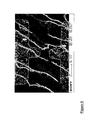
- Figure 1 shows a backscattered electron picture of two electrodes 10 and a system of DNA-templated nanowires 20, 22, 24, which were made highly conductive by selective, self-assembly driven metallisation, whereas this picture is taken by directing an electron beam onto the system to be inspected and by detecting the backscattered electrons according to one aspect of the invention.
- the backscattered picture shown in figure 1 has been achieved with a beam voltage of 4 kV and a working distance WD of 6 mm.
- the DNA-templated nanoscaled wires are randomly aligned, however, for circuits in e.g. nanoelectronics, better defined alignments can be realized.
- the DNA-templated nanowires 20, 22, 24 do show either a bright contrast or a weak contrast.
- Those wire parts 22 which are electrically connected to at least one electrode 10 show a bright contrast whereas those wire parts 24, which obviously have no direct electrical contact to one of the electrodes 10, appear with a weak contrast.
- Figure 2a shows the system of figure 1 for better comparison and figure 2b shows the same system after an additional defect 32, indicated also by a white circle, has been introduced into the system by an AFM (atomic force microscope) tip assisted cutting of a conducting part of the DNA-templated wire.
- AFM atomic force microscope
- Figure 3 shows an enlarged detail of a backscattered electron picture with DNA-templated nanowires 22 connected to electrodes (not shown) and therefore showing a bright contrast and with DNA-templated nanowires 24, not being connected to electrodes (not shown) and therefore showing only a weak contrast.
- a defect 30 could be detected, separating nanowires 24 not being in contact with an electrode (weak contrast, above defect 30) and nanowires 22, being connected to an electrode (bright contrast, below defect 30).
- the method for defect and conductivity engineering can also be applied independently on the method or the step of inspecting said conductivity nanoscaled structure by a backscattered electron picture, although this combination is, as mentioned above, preferred, as by a combination leading to inventive combinatory advantages.
- the conducting nanoscaled structure can however e.g. also be inspected, in order to e.g. find defects or segments of reduced conductivity, by e.g. optical or infrared variations or by electrical measurements or also by structural investigations using atomic force microscopy.
- FIG. 5 schematically shows some of the main elements of an embodiment of an SEM system used for the inventive method.
- a primary electron beam 102 is generated by an electron source 100, whereas the acceleration voltage can be adjusted in a wide area, being preferably, according to the inventive method, in the range of 1 kV to 10 kV.
- the primary electron beam 102 is directed onto a sample 200 having a nanoscaled structure.
- the sample 200 is shown only schematically, having two electrodes 230 attached on the upper surface of the sample 200.
- the primary electron beam 102 directed onto the sample 200 shows effects mainly within an interaction volume 210 in the sample.
- the interaction volume 210 is shown only schematically in this drawing and is dependent of the material of the sample 200 and the parameters of the electron beam.
- the primary electron beam 102 generates backscattered electrons 150 and secondary electrons 160, whereas the backscattered electrons 150, having essentially the same energy as the primary beam electrons 102, are backscattered essentially in a direction being opposite to the primary electron beam, whereas the secondary electrons 160 are generated in a sideward direction, as schematically indicated in figure 5.
- the direction of the electrons is controlled by magnetic lenses 110 and electrostatic lenses 120 of the SEM.
- the SEM shown in figure 5 comprises an annular detector 170 for backscattered electrons 102, so that a signal for the backscattered electrons can be taken directly and a "backscattered electron picture" can be generated.
- the SEM can of course also comprises a detector for the secondary electrons 160 preferably a lateral detector. It should be mentioned at this point that the secondary electrons 160 are generated only in a secondary emission region 220 in the upper surface region of the sample 200 as schematically indicated in figure 5.
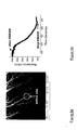
- Fig. 6 shows an SEM image of a single metallized DNA nanowire on a polysterene surface with several nanowires, whereas one of the nanowires, indicated by arrows, has been utilized for obtaining the measurement results shown in Fig. 7.
- Fig. 7 shows the data obtained during the so-called “current-annealing" of this wire, i.e. the result obtained during biasing this wire with a certain current density according to the invention.
- the current density J D was adjusted to provide a decreasing resistivity over time.
- the initial bias voltage of 0,1 V led to a current of 1,24 mA and a current density of 9,34 * 10 10 A/m 2 (taking into account the wire length of 6,5 ⁇ m and a diameter of 130 nm).
- the resistance was stable at a level of about 80,4 Q.
- the current has been increased to 2,32 mA, giving a current density of 1,78 * 10 11 A/m 2 .
- the resistance tremendously decreases versus time. Only after biasing the system with a bias voltage of 0,2 V for 40 seconds, whereafter the bias voltage was returned to 0,1 V, the wire resistance has irreversibly dropped from 80,4 ⁇ to 76,6 ⁇ , which corresponds to a reduction of about 4,7%.
- the resistance can be further decreased by again applying a bias voltage of about 0,2 V, as explained above.
- Fig. 8a shows a metallized DNA wire on a polysterene substrate between two electrodes. An electron beam at 5 kV (apertures between 30 and 120 ⁇ m) was focused on the wire area.
- Fig. 8b shows a change of the resistance of the wire plus electrodes versus an electronic beam treatment time for different apertures.
- an aperture of 30 ⁇ m and 60 ⁇ m corresponding to a beam current of 100 pA and 250 pA, the change of the resistance versus time has been very small.
- the irradiated area was about 1,05 * 10 -7 cm 2 , therefore the corresponding current density was 9,5 * 10 -4 A/cm 2 for 100 pA and 2,4 * 10 -3 A/cm 2 for 250 pA.
- the aperture has been increased to 120 ⁇ m (corresponding to a beam current of 600 pA), a significant change of the wire resistivity has been initiated, as can be clearly seen in the graph of fig. 8b.
- the corresponding density was 5,7 * 10 -3 A/cm 2 in this case.
- the resistance decreased in total from 82,2 ⁇ to 80,5 Q, corresponding to about 2% decrease.
- Fig. 9a shows a further example and a defect in a metallized DNA wire, which has been detected by applying an external voltage to the electrodes.
- An electron beam at 5 kV (aperture 120 ⁇ m, beam current 600 pA) was focused on the defective area.
- the focused area was estimated to be about 90 nm 2 . This gives a current density of about 66,7 A/cm 2 .
- Fig. 9b shows the change of the resistance versus the time during which the electronic beam treatment has been applied.
- the resistance of the DNA wire starts to decrease immediately when the electronic beam has been switched on and still stays at the lower level even after the electronic beam has been switched off again, clearly indicating that the decreasing of the resistance will be maintained permanently.
- Figs. 10a and 10 b show a similar example as shown in Fig. 9.
- Fig. 10a is an SEM picture of a DNA wire with a clear defect in the center. An electron beam at 5 kV (aperture 60 ⁇ m, beam current 250pA) was focused on the defective area. The current density was about 27,8 A/cm 2 .
- Fig. 10b shows, similarly to Fig. 9b, the change of the resistance versus time during which the electron beam treatment has taken place.
- the resistance of the DNA wire decreases when the electron beam is switched on and saturates at a lower level. It has to be noticed here that there is a saturation even in case the electronic beam treatment is continued, as it is shown in this case.
- the overall resistance decreases by a factor of about 12,6, namely from 139 k ⁇ to 11 k ⁇ .
- Figs. 11a and 11b show a still further example, whereas Fig. 11a shows an SEM picture of a DNA wire that had a high contact resistance to the lower electrode, as has been determined in an external biasing experiment. The image shows the situation when a voltage of -5V was applied to the upper electrode.
- an electron beam at 5kV (aperture 120 ⁇ m, beam current 1 nA) was focussed onto the defective area.
- the current density was at a range of about 111 A/cm 2 .
- Fig. 11b shows the decrease of the resistance (log-scale) versus time during which an electron beam treatment took place.
- the resistance of the DNA wire decreases during the time in which an electron beam is switched on, and the resistance of the DNA wire saturates at a lower level.
- the overall resistance decreased by a factor of about 100 from 100 k ⁇ to 1 k ⁇ .
Landscapes
- Engineering & Computer Science (AREA)
- Chemical & Material Sciences (AREA)
- Physics & Mathematics (AREA)
- Nanotechnology (AREA)
- Plasma & Fusion (AREA)
- Analytical Chemistry (AREA)
- Mathematical Physics (AREA)
- Theoretical Computer Science (AREA)
- Crystallography & Structural Chemistry (AREA)
- Internal Circuitry In Semiconductor Integrated Circuit Devices (AREA)
- Testing Or Measuring Of Semiconductors Or The Like (AREA)
- Analysing Materials By The Use Of Radiation (AREA)
Abstract
Description
Depending on the current density JD,I applied, the conductivity or resistivity can be decreased or increased, whereas a lower current density JD is preferably used for decreasing resistivity and a higher current density JI is utilized for increasing resistivity.
- Fig. 1
- shows a backscattered electron picture of nanoscaled metallised DNA-wires connected to electrons;
- Fig. 2
- shows a backscattered electron picture of the system shown in figure 1 before (Figure 2a) and after cutting a nanoscaled metallised DNA-wire (Figure 2b);
- Fig. 3
- shows an enlarged detail of a backscattered electron picture of a nanoscaled metallised DNA wire system with a defect in a single metallised DNA-templated nanowire;
- Fig. 4
- shows the same enlarged detail of the backscattered electron picture of the system shown in figure 3 after the defect in the single metallised DNA-templated nanowire has been repaired;
- Fig. 5
- shows a schematic drawing of an embodiment SEM adopted to the inventive method with indicated paths of backscattered and secondary electrons.
- Fig. 6
- shows an SEM image of a single metallized DNA nanowire on a polysterene surface, whereas this metallized DNA has been "current-annealed " according to the invention;
- Fig. 7
- shows the resistance versus time during a current-annealing treatment according to the invention of a metallized DNA wire according to Fig. 6;
- Fig. 8a
- shows a further SEM picture of a DNA wire;
- Fig. 8b
- shows the resistance versus time during an electron-beam assisted fusing process of the entire wire according to the invention;
- Fig. 9a
- shows a further SEM picture of a system with a defect location;
- Fig. 9b
- shows a resistance versus time for an electron-beam assisted fusion process of the system shown in Fig. 9a according to the invention;
- Fig. 10a
- shows a further SEM picture of a defect location;
- Fig. 10b
- shows a resistance versus time for an electron-beam assisted fusion process of the system shown in Fig. 10a according to the invention;
- Fig. 11a
- shows an SEM picture of a further defect location;
- Fig. 11b
- shows a resistance versus time for an electron-beam assisted fusion process of the system shown in Fig. 11 a according to the invention.
- 10
- electrode
- 20
- nanowire
- 22
- nanowire
- 24
- nanowire
- 30
- defect
- 32
- defect
- 34
- defect
- 35
- repaired defect
- 100
- electron source
- 102
- primary electron beam
- 110
- magnetic lenses
- 120
- electrostatic lenses
- 150
- backscattered electrons
- 160
- secondary electrons
- 170
- detector for backscattered electrons
- 200
- sample (with nanoscaled structure)
- 210
- interaction volume
- 220
- secondary emission region
- 230
- electrodes
Claims (30)
- Method for defect and conductivity engineering of a conducting nanoscaled structure or at least a part of itby generating heat-induced migration, melting, sputtering and/or evaporation of conductive material of the nanoscaled structure by directing a focused electron beam on the nanoscaled structure or an individual portion of it to be engineered and/orby applying one or multiple wires of the conducting nanoscaled structure by applying a current density JD,I whereas the current density JD,I has a value below a critical current density JC, which is the current per cross-section area of the wire at which the wire fails due to overheating and electromigration, and not lower than 3 orders of magnitude below said critical current density JC.
- Method according to claim 1, characterized in that a portion of the nanoscaled structure to be engineered is a gap region to be repaired, whereby the focused electron beam is directed onto said gap region including defect edges and generates heat-induced migration, melting, sputtering and/or evaporation of the conductive material of the defect edges into the gap between said defect edges, filing the gap and connecting said defect edges.
- Method according to claim 1 or 2, characterized in that the electron beam has an accelerating beam voltage between 0,1 kV and 50 kV, preferably between 3kV and 10kV.
- Method according to one of the preceding claims, characterized in that the electron beam has a current density of 1 to 100 A/cm2.
- Method according to one of the preceding claims, characterized in that the electron beam has an absolute beam current of 10 to 1000 pA, preferably 20 to 500 pA.
- Method according to one of the preceding claims, characterized in that the electron beam will be applied in a scanning modus with a scanning window having a diameter or side lengths between 10 nm and 100 nm.
- Method according to claim 6, characterized in that an individual portion of the conducting nanoscaled structure to be engineered is centered in the scanning window.
- Method according to one of the preceding claims, characterized in that the electron beam has a beam diameter of 1 to 50 nm.
- Method according to one of the preceding claims, characterized in that a working distance to the conducting nanoscaled structure is between 2 mm and 10 mm.
- Method according to one of the preceding claims, characterized in that an electron doses of totally 1 to 500 mC/cm2 is applied for the engineering of one individual portion.
- Method according to one of the preceding claims, also including a step of inspecting said conductivity nanoscaled structure by directing an electron beam onto a portion of the conducting nanoscaled structure to be inspected and detecting backscattered electrons.
- Method according to claim 11, characterized in that during the step of inspecting, a beam of primary electrons is accelerated to high potential by an electric field and retarded by a retarding field before reaching the conducting nanoscaled structure.
- Method according to claim 11 or 12, characterized in that a first detection means only detects backscattered electrons and a second detection means detects both secondary electrons and backscattered electrons.
- Method according to one of the claims 11 to 13, characterized in that the electron beam during the step of inspecting said conducting nanoscaled structure applies an electron doses of totally 0,1 to 10 mC/cm2.
- Method according to one of the claims 11 to 14, characterized in that the electron beam during the step of inspecting has an absolute beam current between 1 pA and 500 pA, preferably between 20 pA and 100 pA.
- Method according to one the claims 11 to 15, characterized in that the electron beam during the step of inspecting has an accelerating beam voltage between 0,01 and 50 kV, preferably between 1 kV and 10kV.
- Method according to claims 11 to 16, characterized in that said retarding field retards the primary electrons of the electron beam to an energy of 2% to 10% of its maximum energy generated by said electric field.
- Method according to one of the preceding claims, characterized in that a focused electron beam is directed onto a conducting nanoscaled structure or a portion of it for a time interval of up to 6000 seconds.
- Method according to one of the preceding claims, characterized in that a focused electron beam is directed onto a conducting nanoscaled structure or a portion of it for a time interval between 1 second and 4000 seconds, especially between 1000 seconds and 2000 seconds.
- Method according to one of the preceding claims, characterized in that the current density JD,I is adjusted to less than one order of magnitude below the critical current density JC.
- Method according to one of the preceding claims, characterized in that a current density JD for decreasing the resistivity of one or multiple wires of the nanoscaled structure is between 0,01 * JC and 0,1 * JC.
- Method according to one of the claims 1 to 21, characterized in that a current density JI for increasing the resistivity of a wire or multiple wires of the nanoscaled structure is higher than the current density JD for decreasing the resistivity.
- Method according to claim 22, characterized in that the current density JI for increasing the resistivity is between 0,1 * JC and 0,9 * JC.
- Method according to one of the preceding claims, characterized in that the wire or multiple wires of the nanoscaled structure are biased by a current density JI or JD for a time interval of up to 5000 seconds.
- Method according to one of the preceding claims, characterized in that the wire or multiple wires of the nanoscaled structure are biased by a current density JI or JD for a time interval shorter than 1000 seconds.
- Method according to one of the preceding claims characterized in that the wire or multiple wires of the nanoscaled structure are biased by a current density JI or JD for a time interval shorter than 500 seconds.
- Method according to one of the preceding claims characterized in that the wire or multiple wires of the nanoscaled structure are biased by a current density JI or JD for a time interval between 1 to 400 seconds, especially between 100 seconds and 250 seconds.
- Use of a scanning electron microscope (SEM) system having a filter for detecting backscattered electrons for a method according to one of the claims 1 to 27.
- Use of a scanning electron microscope system according to claim 28, characterized in that the scanning electron microscope is designed to have an aperture between 10 µm and 100 µm, preferably between 30 µm and 60 µm.
- Use of a scanning electron microscope system according to claim 28 or 29, characterized in that the filter for detecting backscattered electrons comprises an annular backscattered electrons detector (102).
Priority Applications (1)
| Application Number | Priority Date | Filing Date | Title |
|---|---|---|---|
| EP02027938A EP1320117A3 (en) | 2001-12-13 | 2002-12-13 | Method for defect and conductivity engineering of a conducting nanoscaled structure |
Applications Claiming Priority (3)
| Application Number | Priority Date | Filing Date | Title |
|---|---|---|---|
| EP01129710 | 2001-12-13 | ||
| EP01129710 | 2001-12-13 | ||
| EP02027938A EP1320117A3 (en) | 2001-12-13 | 2002-12-13 | Method for defect and conductivity engineering of a conducting nanoscaled structure |
Publications (2)
| Publication Number | Publication Date |
|---|---|
| EP1320117A2 true EP1320117A2 (en) | 2003-06-18 |
| EP1320117A3 EP1320117A3 (en) | 2003-11-26 |
Family
ID=26076795
Family Applications (1)
| Application Number | Title | Priority Date | Filing Date |
|---|---|---|---|
| EP02027938A Withdrawn EP1320117A3 (en) | 2001-12-13 | 2002-12-13 | Method for defect and conductivity engineering of a conducting nanoscaled structure |
Country Status (1)
| Country | Link |
|---|---|
| EP (1) | EP1320117A3 (en) |
Family Cites Families (5)
| Publication number | Priority date | Publication date | Assignee | Title |
|---|---|---|---|---|
| IL83038A (en) * | 1987-06-30 | 1991-08-16 | Aaron Lewis | Method and device for submicron precision pattern generation |
| GB8911394D0 (en) * | 1989-05-18 | 1989-07-05 | Spence John | Electron beam machining of materials |
| US5504340A (en) * | 1993-03-10 | 1996-04-02 | Hitachi, Ltd. | Process method and apparatus using focused ion beam generating means |
| US6322672B1 (en) * | 2000-03-10 | 2001-11-27 | Fei Company | Method and apparatus for milling copper interconnects in a charged particle beam system |
| US6821682B1 (en) * | 2000-09-26 | 2004-11-23 | The Euv Llc | Repair of localized defects in multilayer-coated reticle blanks for extreme ultraviolet lithography |
-
2002
- 2002-12-13 EP EP02027938A patent/EP1320117A3/en not_active Withdrawn
Also Published As
| Publication number | Publication date |
|---|---|
| EP1320117A3 (en) | 2003-11-26 |
Similar Documents
| Publication | Publication Date | Title |
|---|---|---|
| KR100686294B1 (en) | Electron source with carbon nanotubes and electron microscope and electron beam drawing device using it | |
| JP4088533B2 (en) | Sample preparation apparatus and sample preparation method | |
| US20100187433A1 (en) | Improved particle beam generator | |
| US6888150B2 (en) | Method for defect and conductivity engineering of a conducting nanoscaled structure | |
| US20100193687A1 (en) | Field emission type electron gun comprising single fibrous carbon electron emitter and operating method for the same | |
| US7759160B2 (en) | Method for producing conductor structures and applications thereof | |
| JP5236501B2 (en) | Nano manufacturing equipment and nano manufacturing method | |
| US20040169142A1 (en) | Method for analyzing organic material per microscopic area, and device for analysis per microscopic area | |
| Li et al. | Low-current focused-ion-beam induced deposition of three-dimensional tungsten nanoscale conductors | |
| JP5102968B2 (en) | Conductive needle and method of manufacturing the same | |
| Gupta et al. | Conducting ion tracks generated by charge-selected swift heavy ions | |
| EP4001970A1 (en) | Radiation detector | |
| RU2194334C1 (en) | Method for producing nanometric-size ferrite conductor | |
| JP3453325B2 (en) | Semiconductor device and manufacturing method thereof | |
| US8887381B2 (en) | Method of making a 3-D structure | |
| DE19802779A1 (en) | Electron emitter device for e.g. display | |
| Brückl et al. | Observation of Coulomb Blockade Effects in AFM‐machined Tunnel Junctions | |
| JP5804415B2 (en) | Nano-gap electrode and manufacturing method thereof | |
| Sapkov et al. | Method of creation of monomolecular transistor with overhanging electrodes | |
| von Gratowski et al. | Creation of the Nano-Soldering Technology for 3D Mechanical Bottomup Nano-Assembling of Individual Nanodevices | |
| Orús | Nanofabrication of metallic and superconducting tungsten-carbon nanostructures using focused ion beams | |
| Krauser et al. | Graphitic nanowires embedded in diamond-like carbon films | |
| Panitz | Electrostatic removal of lithium fluoride from field‐emitter tips at elevated temperatures | |
| Neklyudova | In situ TEM electrical measurements of semiconductor and metal nanowires | |
| JP2003017241A (en) | Micro light emitting device and method of manufacturing the same |
Legal Events
| Date | Code | Title | Description |
|---|---|---|---|
| PUAI | Public reference made under article 153(3) epc to a published international application that has entered the european phase |
Free format text: ORIGINAL CODE: 0009012 |
|
| AK | Designated contracting states |
Designated state(s): AT BE BG CH CY CZ DE DK EE ES FI FR GB GR IE IT LI LU MC NL PT SE SI SK TR |
|
| AX | Request for extension of the european patent |
Extension state: AL LT LV MK RO |
|
| PUAL | Search report despatched |
Free format text: ORIGINAL CODE: 0009013 |
|
| AK | Designated contracting states |
Kind code of ref document: A3 Designated state(s): AT BE BG CH CY CZ DE DK EE ES FI FR GB GR IE IT LI LU MC NL PT SE SI SK TR |
|
| AX | Request for extension of the european patent |
Extension state: AL LT LV MK RO |
|
| 17P | Request for examination filed |
Effective date: 20040517 |
|
| AKX | Designation fees paid |
Designated state(s): DE FR GB NL |
|
| RAP1 | Party data changed (applicant data changed or rights of an application transferred) |
Owner name: SONY DEUTSCHLAND GMBH |
|
| 17Q | First examination report despatched |
Effective date: 20060810 |
|
| RAP1 | Party data changed (applicant data changed or rights of an application transferred) |
Owner name: SONY DEUTSCHLAND GMBH |
|
| STAA | Information on the status of an ep patent application or granted ep patent |
Free format text: STATUS: THE APPLICATION IS DEEMED TO BE WITHDRAWN |
|
| 18D | Application deemed to be withdrawn |
Effective date: 20100701 |