EP1320019A2 - Clock signal supply circuit - Google Patents
Clock signal supply circuit Download PDFInfo
- Publication number
- EP1320019A2 EP1320019A2 EP02258423A EP02258423A EP1320019A2 EP 1320019 A2 EP1320019 A2 EP 1320019A2 EP 02258423 A EP02258423 A EP 02258423A EP 02258423 A EP02258423 A EP 02258423A EP 1320019 A2 EP1320019 A2 EP 1320019A2
- Authority
- EP
- European Patent Office
- Prior art keywords
- circuit
- clock signal
- waveform shaping
- signal supply
- sine wave
- Prior art date
- Legal status (The legal status is an assumption and is not a legal conclusion. Google has not performed a legal analysis and makes no representation as to the accuracy of the status listed.)
- Withdrawn
Links
Images


Classifications
-
- G—PHYSICS
- G06—COMPUTING OR CALCULATING; COUNTING
- G06F—ELECTRIC DIGITAL DATA PROCESSING
- G06F1/00—Details not covered by groups G06F3/00 - G06F13/00 and G06F21/00
- G06F1/04—Generating or distributing clock signals or signals derived directly therefrom
- G06F1/10—Distribution of clock signals, e.g. skew
Definitions
- the present invention relates to a supply circuit of a clock signal in, for example, a computer.
- Fig. 4 shows a conventional clock signal supply circuit 1.
- a clock signal outputted from a clock signal generator 35 is supplied to circuit units provided in the inside of a personal computer (called pasokon), such as a CPU 31, a memory 32, a video card 33, and a sound card 34.
- the clock signal generator 35 outputs a rectangular wave, and is mounted on a mother board 36 in the personal computer as shown in Fig. 5.
- the CPU 31 or the memory 32 is constructed as an integrated circuit, and is mounted on the mother board 36.
- the video card 33 or the sound card 34 is made of a dedicated card-type board on which an image processing circuit or a sound processing circuit is constructed.
- Connectors 37 are attached on the mother board 36, and these cards are mounted to the mother board 36 through the connectors 37.
- a wiring conductor (not shown), which becomes a bus, is formed on the mother board 36, and the clock signal is supplied to the respective circuit devices through this wiring conductor.
- the clock signal is transmitted on the mother board and is inputted to the respective circuit devices.
- the rectangular wave includes many higher harmonics as is generally known, and as shown in Fig. 6, the levels of odd harmonics are especially high. Thus, they easily leak out of the personal computer, and there has been a problem that they interfere with other electronic equipment.
- the invention has an object to realize a circuit for preventing odd harmonics of a clock signal from leaking out of an equipment, such as a personal computer, using the clock signal.
- a circuit of the invention includes a sine wave oscillator and a circuit operating with an oscillation signal, as a clock signal, outputted from the sine wave oscillator, and is characterized in that a waveform shaping circuit is provided correspondingly to the circuit, the circuit and the waveform shaping circuit are constructed in a same circuit unit, and the oscillation signal is converted into a rectangular wave by the waveform shaping circuit in the circuit unit and is supplied to the circuit.
- the circuit unit is an integrated circuit constituting a circuit such as a CPU or a memory.
- the circuit unit may be a dedicated card-type board constituting a circuit such as a sound processing circuit or an image processing circuit.
- the sine wave oscillator is constituted by a PLL synthesizer.
- Fig. 1 is a block diagram showing a structure of a clock signal supply circuit of the invention.
- Fig. 2 is a structural view of the inside of a personal computer for explaining the clock signal supply circuit of the invention.
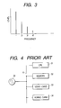
- Fig. 3 is a view showing radiation levels of higher harmonics in the clock signal supply circuit of the invention.
- Fig. 4 is a block diagram showing a structure of a conventional clock signal supply circuit.
- Fig. 5 is a structural view in the inside of a personal computer for explaining the conventional clock signal supply circuit.
- Fig. 6 is a view showing radiation levels of higher harmonics in the conventional clock signal supply circuit.
- Fig. 1 shows a clock signal supply circuit of the invention.
- Circuit units such as a CPU IC (integrated circuit constituting a CPU) 1, a memory IC (integrated circuit constituting a memory) 2, a video card 3, and a sound card 4, and a clock oscillator (sine wave oscillator) 5 are provided in the inside of a personal computer (called pasokon) or the like.
- a waveform shaping circuit 1b is constructed in the inside of the CPU IC 1, in addition to a main body circuit 1a of the CPU comprised of a control unit and an arithmetic unit.
- a waveform shaping circuit 2b is constructed in the inside of the memory IC 2, in addition to a main body circuit 2a of the storage device.
- the video card 3 includes an image processing circuit 3a and a waveform shaping circuit 3b constructed on a dedicated card-type board
- the sound card 4 includes a sound processing circuit 4a and a waveform shaping circuit 4b constructed on a dedicated card-type board.
- the clock oscillator 5 is constituted by a PLL-controlled frequency synthesizer or the like, and outputs an oscillation signal of a sine wave. Then, the oscillation signal is supplied to the respective circuit units, such as the CPU IC 1, the memory IC 2, the video card 3, and the sound card 4, through a bus 6.
- the CPU IC 1, the memory IC 2, and the clock oscillator 5 are mounted on a mother board 7 in the personal computer as shown in Fig. 2.
- a connector 8 is attached on the mother board 7, and the video card 3 or the sound card 4 is mounted to the mother board 7 through the connector 8.
- a wiring conductor 7a, which becomes the bus 6, is formed on the mother board 7, and the oscillation signal outputted from the clock oscillator 5 is transmitted through this wiring conductor 7a and is supplied to the respective circuit units 1, 2, 3 and 4.
- the oscillation signal supplied to each of the circuit units 1, 2, 3 and 4 is first converted into a rectangular wave by each of the waveform shaping circuits 1b, 2b, 3b and 4b, and is supplied to each of the main body circuit 1a of the CPU, the memory main body circuit 2a, the video processing circuit 3a, and the sound processing circuit 4a, in the same circuit unit.
- the oscillation signal (fundamental frequency f) of the sine wave is transmitted on the mother board 7, the levels of higher harmonics radiated from the wiring conductor 7a, especially those of odd harmonics become low as shown in Fig. 3, and they do not interfere with other circuits in the personal computer, and further, higher harmonics leaking out of the personal computer also lessen.
- the clock signal supply circuit of the invention includes a sine wave oscillator and a circuit operating with an oscillation signal, as a clock signal, outputted from the sine wave oscillator, a waveform shaping circuit is provided correspondingly to the circuit, the circuit and the waveform shaping circuit are constructed in a same circuit unit, and the oscillation signal is converted into a rectangular wave by the waveform shaping circuit in the circuit unit, whereby the oscillation signal having low level higher harmonics is transmitted from the sine wave oscillator to the circuit unit. Accordingly, higher harmonics radiated therebetween also lessen. Besides, since the oscillation signal transmitted to the circuit unit is converted into the rectangular wave in the circuit unit and is immediately supplied to the circuit, higher harmonics radiated to the outside of the circuit unit also lessen. Accordingly, they do not interfere with other circuits in the equipment, and further, higher harmonics radiated to the outside of the equipment also lessen.
- the circuit unit is an integrated circuit constituting a circuit such as a CPU or a memory
- the oscillation signal is changed into the rectangular wave in the integrated circuit and is supplied to the circuit, and accordingly, higher harmonics radiated to the outside of the integrated circuit also lessen.
- the circuit unit is a dedicated card-type board constituting a circuit such as a sound processing circuit or an image processing circuit, it is changed into the rectangular wave in the card-type board and is supplied to the circuit, and accordingly, higher harmonics radiated to the outside of the card-type board also lessen.
- the sine wave oscillator is constituted by a PLL synthesizer, selection of a frequency of the clock signal can be suitably made correspondingly to each circuit.
Landscapes
- Engineering & Computer Science (AREA)
- Theoretical Computer Science (AREA)
- Physics & Mathematics (AREA)
- General Engineering & Computer Science (AREA)
- General Physics & Mathematics (AREA)
- Stabilization Of Oscillater, Synchronisation, Frequency Synthesizers (AREA)
- Microcomputers (AREA)
- Manipulation Of Pulses (AREA)
- Credit Cards Or The Like (AREA)
- Semiconductor Integrated Circuits (AREA)
Abstract
Description
Claims (4)
- A clock signal supply circuit, comprising:a sine wave oscillator; anda circuit operating with an oscillation signal, as a clock signal, outputted from the sine wave oscillator, characterized in thata waveform shaping circuit is provided correspondingly to the circuit,the circuit and the waveform shaping circuit are constructed in a same circuit unit, andthe oscillation signal is converted into a rectangular wave by the waveform shaping circuit in the circuit unit and is supplied to the circuit.
- A clock signal supply circuit as set forth in claim 1, characterized in that the circuit unit is an integrated circuit constituting a circuit such as a CPU or a memory.
- A clock signal supply circuit as set forth in claim 1, characterized in that the circuit unit is a dedicated card-type board constituting a circuit such as a sound processing circuit or an image processing circuit.
- A clock signal supply circuit as set forth in claim 1, characterized in that the sine wave oscillator is constituted by a PLL synthesizer.
Applications Claiming Priority (2)
| Application Number | Priority Date | Filing Date | Title |
|---|---|---|---|
| JP2001381208A JP2003186565A (en) | 2001-12-14 | 2001-12-14 | Clock signal supply circuit |
| JP2001381208 | 2001-12-14 |
Publications (2)
| Publication Number | Publication Date |
|---|---|
| EP1320019A2 true EP1320019A2 (en) | 2003-06-18 |
| EP1320019A3 EP1320019A3 (en) | 2005-09-28 |
Family
ID=19187305
Family Applications (1)
| Application Number | Title | Priority Date | Filing Date |
|---|---|---|---|
| EP02258423A Withdrawn EP1320019A3 (en) | 2001-12-14 | 2002-12-06 | Clock signal supply circuit |
Country Status (4)
| Country | Link |
|---|---|
| US (1) | US6781430B2 (en) |
| EP (1) | EP1320019A3 (en) |
| JP (1) | JP2003186565A (en) |
| TW (1) | TW583836B (en) |
Families Citing this family (8)
| Publication number | Priority date | Publication date | Assignee | Title |
|---|---|---|---|---|
| JP4787651B2 (en) * | 2006-03-31 | 2011-10-05 | 日本電波工業株式会社 | Clock distribution circuit for digital processing equipment |
| CN102468826B (en) * | 2010-11-03 | 2016-04-06 | 北京普源精电科技有限公司 | A kind of multifunctional signal generator |
| CN102468829B (en) * | 2010-11-03 | 2016-04-06 | 北京普源精电科技有限公司 | A kind of signal generator and wave table recombination method thereof |
| US8878620B2 (en) * | 2012-08-24 | 2014-11-04 | Tektronix, Inc. | Phase coherent playback in and arbitrary waveform generator |
| CN103633967B (en) * | 2013-11-29 | 2016-04-27 | 青岛汉泰电子有限公司 | A kind of digital arbitrary waveform generator |
| CN103973271A (en) * | 2014-04-28 | 2014-08-06 | 苏州经贸职业技术学院 | Signal generation circuit |
| CN105306019A (en) * | 2015-11-23 | 2016-02-03 | 国家电网公司 | Triangular wave generation circuit used for active power filter |
| JP2018142774A (en) * | 2017-02-27 | 2018-09-13 | 国立大学法人東北大学 | Receiver |
Family Cites Families (10)
| Publication number | Priority date | Publication date | Assignee | Title |
|---|---|---|---|---|
| JPS5917781B2 (en) * | 1978-04-03 | 1984-04-23 | 日本電信電話株式会社 | Rotation speed detection method using multipolar resolver |
| JPS5769258A (en) * | 1980-10-20 | 1982-04-27 | Nippon Denshi Kagaku Kk | Automatic capacity balancing circuit device for ac bridge |
| JPS59169222A (en) * | 1983-03-16 | 1984-09-25 | Victor Co Of Japan Ltd | Code generator |
| JPH01124014A (en) * | 1987-11-10 | 1989-05-16 | Sharp Corp | Digital apparatus |
| JPH03129416A (en) * | 1989-10-14 | 1991-06-03 | Hitachi Ltd | Pulse supplying system, integrated circuit, and information processor |
| US5281861A (en) * | 1989-11-30 | 1994-01-25 | Compaq Computer Corporation | Sine wave clock distribution with high voltage output |
| JPH03214307A (en) * | 1990-01-19 | 1991-09-19 | Fujitsu General Ltd | Clock transmission method |
| JPH0786878A (en) | 1993-09-10 | 1995-03-31 | Sony Tektronix Corp | Clock signal generating circuit |
| JPH08129428A (en) * | 1994-10-31 | 1996-05-21 | Fuji Facom Corp | Clock signal supply method |
| JPH10268963A (en) * | 1997-03-28 | 1998-10-09 | Mitsubishi Electric Corp | Information processing device |
-
2001
- 2001-12-14 JP JP2001381208A patent/JP2003186565A/en not_active Withdrawn
-
2002
- 2002-11-27 TW TW091134516A patent/TW583836B/en not_active IP Right Cessation
- 2002-12-06 EP EP02258423A patent/EP1320019A3/en not_active Withdrawn
- 2002-12-06 US US10/313,262 patent/US6781430B2/en not_active Expired - Fee Related
Also Published As
| Publication number | Publication date |
|---|---|
| EP1320019A3 (en) | 2005-09-28 |
| JP2003186565A (en) | 2003-07-04 |
| TW583836B (en) | 2004-04-11 |
| TW200301041A (en) | 2003-06-16 |
| US20030117203A1 (en) | 2003-06-26 |
| US6781430B2 (en) | 2004-08-24 |
Similar Documents
| Publication | Publication Date | Title |
|---|---|---|
| KR940001361B1 (en) | Data processing device | |
| EP0645689A2 (en) | Clock supply system, real-time clock module, and clock generator | |
| US6781430B2 (en) | Clock signal supply circuit with odd harmonic leakage prevention feature | |
| JP2001160663A (en) | Circuit board | |
| US6259291B1 (en) | Self-adjusting apparatus and a self-adjusting method for adjusting an internal oscillating clock signal by using same | |
| TW591359B (en) | Analog/digital hybrid integrated circuit | |
| US6680623B2 (en) | Information processing apparatus having a reduced signal distortion between a module and a memory | |
| US6963990B2 (en) | Clock generation for multiple secondary buses of a PCI bridge | |
| US7114092B2 (en) | Method of supplying a required clock frequency by a clock generator module through interface communication with a mainboard | |
| US20090295490A1 (en) | Dds circuit and electronic device having the same | |
| JP2001345423A (en) | Semiconductor integrated circuit device and method of manufacturing the same | |
| JP2000276250A (en) | Clock signal generation method for universal asynchronous transceiver | |
| EP0212640A2 (en) | Data processor | |
| JP2000156578A (en) | Heat dissipation structure of electronic device | |
| JP2010073792A (en) | Semiconductor device and one-chip microcomputer | |
| JPH10242282A (en) | Wiring structure of signal wiring | |
| JPH05189080A (en) | Portable computer | |
| JP2003318352A (en) | System and semiconductor device | |
| US6948137B2 (en) | Semiconductor integrated device | |
| JP2854194B2 (en) | Oscillation clock judgment device for microcomputer | |
| JPH03224019A (en) | Clock cards and information processing equipment | |
| JPH11177025A (en) | Semiconductor integrated circuit | |
| KR100470827B1 (en) | Method of generating a clock signal for universal asynchronous receiver-transmitter | |
| US20030131275A1 (en) | Microcontroller and system having a clock generator | |
| JP2003108259A (en) | Clock noise removal circuit |
Legal Events
| Date | Code | Title | Description |
|---|---|---|---|
| PUAI | Public reference made under article 153(3) epc to a published international application that has entered the european phase |
Free format text: ORIGINAL CODE: 0009012 |
|
| AK | Designated contracting states |
Designated state(s): AT BE BG CH CY CZ DE DK EE ES FI FR GB GR IE IT LI LU MC NL PT SE SI SK TR |
|
| AX | Request for extension of the european patent |
Extension state: AL LT LV MK RO |
|
| PUAL | Search report despatched |
Free format text: ORIGINAL CODE: 0009013 |
|
| AK | Designated contracting states |
Kind code of ref document: A3 Designated state(s): AT BE BG CH CY CZ DE DK EE ES FI FR GB GR IE IT LI LU MC NL PT SE SI SK TR |
|
| AX | Request for extension of the european patent |
Extension state: AL LT LV MK RO |
|
| 17P | Request for examination filed |
Effective date: 20051125 |
|
| AKX | Designation fees paid |
Designated state(s): DE FR GB |
|
| STAA | Information on the status of an ep patent application or granted ep patent |
Free format text: STATUS: THE APPLICATION IS DEEMED TO BE WITHDRAWN |
|
| 18D | Application deemed to be withdrawn |
Effective date: 20061006 |