EP1319973A1 - Optical device - Google Patents

Optical device Download PDF

Info

Publication number
EP1319973A1
EP1319973A1 EP01965559A EP01965559A EP1319973A1 EP 1319973 A1 EP1319973 A1 EP 1319973A1 EP 01965559 A EP01965559 A EP 01965559A EP 01965559 A EP01965559 A EP 01965559A EP 1319973 A1 EP1319973 A1 EP 1319973A1
Authority
EP
European Patent Office
Prior art keywords
waveguide
optical
branch
cross
clad layer
Prior art date
Legal status (The legal status is an assumption and is not a legal conclusion. Google has not performed a legal analysis and makes no representation as to the accuracy of the status listed.)
Granted
Application number
EP01965559A
Other languages
German (de)
French (fr)
Other versions
EP1319973A4 (en
EP1319973B1 (en
Inventor
Osamu c/o NGK Insulators Ltd. Mitomi
Takenori c/o NGK Insulators Ltd. Ichigi
Masatsugu c/o NGK Insulators Ltd. Oshima
Jun c/o NGK Insulators Ltd. Okumura
Masataka c/o NGK Insulators Ltd. Yamashita
Current Assignee (The listed assignees may be inaccurate. Google has not performed a legal analysis and makes no representation or warranty as to the accuracy of the list.)
NGK Insulators Ltd
Original Assignee
NGK Insulators Ltd
Priority date (The priority date is an assumption and is not a legal conclusion. Google has not performed a legal analysis and makes no representation as to the accuracy of the date listed.)
Filing date
Publication date
Application filed by NGK Insulators Ltd filed Critical NGK Insulators Ltd
Publication of EP1319973A1 publication Critical patent/EP1319973A1/en
Publication of EP1319973A4 publication Critical patent/EP1319973A4/en
Application granted granted Critical
Publication of EP1319973B1 publication Critical patent/EP1319973B1/en
Anticipated expiration legal-status Critical
Expired - Lifetime legal-status Critical Current

Links

Images

Classifications

    • GPHYSICS
    • G02OPTICS
    • G02FOPTICAL DEVICES OR ARRANGEMENTS FOR THE CONTROL OF LIGHT BY MODIFICATION OF THE OPTICAL PROPERTIES OF THE MEDIA OF THE ELEMENTS INVOLVED THEREIN; NON-LINEAR OPTICS; FREQUENCY-CHANGING OF LIGHT; OPTICAL LOGIC ELEMENTS; OPTICAL ANALOGUE/DIGITAL CONVERTERS
    • G02F1/00Devices or arrangements for the control of the intensity, colour, phase, polarisation or direction of light arriving from an independent light source, e.g. switching, gating or modulating; Non-linear optics
    • G02F1/29Devices or arrangements for the control of the intensity, colour, phase, polarisation or direction of light arriving from an independent light source, e.g. switching, gating or modulating; Non-linear optics for the control of the position or the direction of light beams, i.e. deflection
    • G02F1/31Digital deflection, i.e. optical switching
    • G02F1/313Digital deflection, i.e. optical switching in an optical waveguide structure
    • G02F1/3137Digital deflection, i.e. optical switching in an optical waveguide structure with intersecting or branching waveguides, e.g. X-switches and Y-junctions
    • GPHYSICS
    • G02OPTICS
    • G02BOPTICAL ELEMENTS, SYSTEMS OR APPARATUS
    • G02B6/00Light guides; Structural details of arrangements comprising light guides and other optical elements, e.g. couplings
    • G02B6/10Light guides; Structural details of arrangements comprising light guides and other optical elements, e.g. couplings of the optical waveguide type
    • G02B6/12Light guides; Structural details of arrangements comprising light guides and other optical elements, e.g. couplings of the optical waveguide type of the integrated circuit kind
    • G02B6/122Basic optical elements, e.g. light-guiding paths
    • G02B6/1228Tapered waveguides, e.g. integrated spot-size transformers
    • GPHYSICS
    • G02OPTICS
    • G02BOPTICAL ELEMENTS, SYSTEMS OR APPARATUS
    • G02B6/00Light guides; Structural details of arrangements comprising light guides and other optical elements, e.g. couplings
    • G02B6/10Light guides; Structural details of arrangements comprising light guides and other optical elements, e.g. couplings of the optical waveguide type
    • G02B6/12Light guides; Structural details of arrangements comprising light guides and other optical elements, e.g. couplings of the optical waveguide type of the integrated circuit kind
    • G02B6/122Basic optical elements, e.g. light-guiding paths
    • G02B6/125Bends, branchings or intersections

Definitions

  • the present invention relates to an optical device included in a photonic network utilizing a wavelength division multiplex (WDM) method, for example.
  • WDM wavelength division multiplex
  • an optical device for example, an optical switch using an optical waveguide, an optical waveguide device such as an optical modulator and so on tends to be often used.
  • an optical switch includes a first type using a directional coupler or a Mach-Zender interference waveguide and a second type using a branch/cross waveguide.
  • the first type of the optical switch operates analogically, for example, as the voltage to be applied for its switching operation increases, the intensity of the output light from the switch gradually reduces to around zero, after then as the voltage increases furthermore, the intensity increases again.
  • the second type of the optical switch operates digitally in general, and performs an on-off operation by applying the voltage not less than a certain value.
  • the first type of the optical switch performs an on-off operation by changing the phase of light waves propagating in a waveguide. Therefore, for example, as the first type of the optical switch can perform the switching operation only by slightly changing the refractive index of a waveguide with an electro-optical effect, the first type of the optical switch has an advantage to make the operating voltage of the first type of the optical switch small and have a comparatively high operation efficiency.
  • the first type of the optical switch has a disadvantage to have a comparative large size of necessity. Also, in order to perform the on-off operation, it is necessary to set the operating voltage of the first type of the optical switch at an appropriate value according to the switching characteristic of the first type of the optical switch. As a result, an electronic circuit for controlling the optical switch has a complex construction, particularly, in case of a device having a plurality of switch elements such as a matrix switch, it is necessary to perform a fine adjustment of the voltage to each switch.
  • the second type of the optical switch has an advantage to have a comparative small size. As it is enough to apply the voltage not less than a certain value in order to perform the switching operation, the second type of the optical switch has an advantage to omit an electric circuit for control and to control easily compared with the first type of the optical switch.
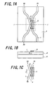
  • Figure 1A is a top view of such a first type of the optical device
  • Figure 1B is a diagram showing a section I-I of Figure 1A
  • Figure 1C is a diagram showing a part surrounded by a dashed line in Figure 1A.
  • This optical device includes a core layer 1 with a cross waveguide, a clad layer 2, an electrode 3 disposed on the cross waveguide and a substrate 4, with the clad layer 2 being deposited on the substrate 4.
  • This optical device utilizes the total reflection phenomenon of light in the switching operation. That is, when a certain voltage is applied to or a certain current is supplied to the electrode 3, the refractive index of a waveguide just under the electrode 3 is changed by an electro-optical (EO) effect or a thermo-optical (TO) effect of a material composing the waveguide.
  • EO electro-optical
  • TO thermo-optical
  • an input light P0 to the waveguide goes straight in the waveguide to become an output light P1, or is totally reflected by the surface just under the electrode 3 to become an output light P2.
  • the branch/cross waveguide has a comparative large sectional area
  • the optical confinement effect in the waveguide is remarkable strong, and thus so-called a multi-mode waveguide performing the propagation in a plurality of modes is formed.
  • the radiation loss or coupling loss to the optical output waveguide caused by such a conversion increases, and thus the optical device may have a remarkable large loss.
  • the amount of variation in refractive index is in proportion to the distribution of the temperature so that the electrode 3 has the highest temperature. Therefore, as the total reflection surface of light formed by changing the refractive index of the waveguide is the same in shape as this distribution of the temperature, and is not perpendicular but inclined to the surface of the clad layer 2, a part of the light reflected by the total reflection surface is emitted from the waveguide, and thus the loss increases. Also, such a part of light may couple to the optical output waveguide opposite to the optical input waveguide, and the crosstalk may degrade.
  • the object of the present invention is to provide an optical device capable of reducing the optical loss and the crosstalk as well as improving the operating efficiency.
  • an optical device comprising;
  • the coupling loss with the optical element or the optical waveguide to be connected to the optical input waveguide and the radiation loss in the connection waveguide reduce in accordance with the reduction of the spot size of a light due to the increasing of the optical confinement.
  • the optical output waveguide or the connection waveguide makes the optical confinement strong and makes the diffraction of the light small, the optical loss and the crosstalk of the optical device reduce.
  • it is preferable to make a branch angle small it is possible to improve the operating efficiency of the optical device because it is possible to have a relative small branch angle without affecting the optical loss and the crosstalk by having a relative large spot size of the light propagating through the branch/cross waveguide.
  • the branch/cross waveguide means a branch waveguide or a cross waveguide.
  • the spot size of light propagating through the branch/cross waveguide is preferably not less than 5 ⁇ m, and the spot size of the light propagating through the optical input waveguide, the optical output waveguide or the connection waveguide is preferably less than 5 ⁇ m.
  • Another optical device according to the present invention comprises;
  • the spot size of the light propagating through a branch/cross waveguide not less than 5 ⁇ m in the present invention, it is possible to make the optical confinement in the optical input waveguide, the branch/cross optical waveguide or the connection waveguide strong and make the diffraction of the light in the branch/cross optical waveguide small, and thus the optical loss and the crosstalk of the optical device reduce regardless of the spot size of the light propagating through the optical input waveguide, the optical output waveguide or the connection waveguide.
  • the width and the thickness of said branch/cross waveguide at a value smaller than the width or the thickness of the optical input waveguide and the optical output waveguide, and/or to set the ratio of width to the thickness of the branch/cross waveguide not less than 10/4.
  • Another optical device of the present invention comprises;
  • Another optical device of the present invention comprises;
  • the width and the thickness of the branch/cross waveguide are not less than 10 ⁇ m and not more than 4 ⁇ m, respectively, and more preferably, the cross/branch angle of the branch/cross waveguide is 3 to 6 degrees.
  • the branch/cross waveguide consists of a single-mode waveguide, for example.
  • the branch/cross waveguide has a tapered waveguide.
  • the optical loss can be reduced.
  • the optical input waveguide and the optical device such as a plane light circuit (PLC) and a semiconductor optical device or the optical waveguide such as an optical fiber by the spot size of the light input into the optical input waveguide substantially equal to the spot size of the light output from an optical element or an optical waveguide to be connected to the optical input waveguide.
  • PLC plane light circuit
  • spot size of the light output from the optical output waveguide is substantially equal to the spot size of the light input into the optical element or the optical waveguide to be connected to the optical output waveguide, it is possible to reduce the coupling loss between the optical output waveguide and the optical device or the optical waveguide.
  • the device of the present invention may further comprise an optical switch for switching over the direction of propagation of light input into the branch/cross waveguide, in this case, the optical switch hsa at least one electrode for changing the refractive index of the branch/cross waveguide by applying a certain voltage or supplying a certain current, for example.
  • Another optical device according to the present invention comprises;
  • the total reflection surface may be substantially perpendicular to the surface of the second clad layer.
  • the loss reduces because the light reflected by the total reflection surface does not substantially emit from a waveguide.
  • the degradation of the crosstalk result from the coupling of a part of the light into the optical output waveguide opposite to the optical input waveguide.
  • the thickness of the first clad layer is preferably between 4 ⁇ m and 40 ⁇ m, and more preferably between 4 ⁇ m and 15 ⁇ m.
  • a core layer with a single-mode optical waveguide does not have a remarkable strong optical confinement effect because of a comparative small sectional area of the core layer, and is generally called a flat core layer.
  • the core layer may have a single-mode optical input waveguide, a single-mode branch/cross waveguide and a single-mode optical output waveguide,
  • the ratio of the width of the electrode to that of the optical waveguide is relatively large, it is possible to have a substantially small excess loss and to have a relatively large extinction ratio of the switching because the optical confinement is not remarkably strong.
  • the ratio of the width of the electrode to that of the optical waveguide is established by the relation between the temperature of the electrode and the driving power.
  • each of the first clad layer and the second clad layer consists of a material having a negative temperature coefficient, and the refractive index of the first clad layer is lower than that of the second clad layer.
  • each of the first clad layer and the second clad layer consists of a material having a positive temperature coefficient, and the refractive index of the first clad layer is higher than that of the second clad layer.
  • optical device using a flat core as the core layer is described, but the optical device is not limited to this as long as it is not described in particular.
  • Figure 2A is a top view of a first embodiment of the optical device according to the present invention, and Figure 2B shows a section II-II of Figure 2A.
  • This optical device formed as a 1 x 2 optical switch includes a core layer 11, a clad layer 12, an electrode 13 disposed on a cross waveguide and a substrate 14, with the clad layer 12 being deposited on the substrate 14.
  • the core layer 11 has optical input waveguides 21a and 21b, a cross waveguide 22, optical output waveguides 23a and 23b, connection waveguides 24a and 24b respectively for connecting the optical input waveguide 21a and the cross waveguide 22 and connecting the optical input waveguide 21b and the cross waveguide 22, and connection waveguides 25a and 25b respectively for connecting the optical output waveguide 23a and the cross waveguide 22 and connecting the optical output waveguide 23b and the cross waveguide 22.
  • the connection waveguides 24a, 24b, 25a and 25b have curved waveguides 26a, 26b, 27a and 27b, and tapered waveguides 28a, 28b 29a and 29b, respectively.
  • Each of these optical input waveguides 21a and 21b, cross waveguide 22, optical output waveguides 23a and 23b, and connection waveguides 24a, 24b, 25a and 25b is a single-mode optical waveguide.
  • the width of the cross waveguide 22 is smaller than those of the optical input waveguides 21a and 21b, the optical output waveguides 23a and 23b, and the curved waveguides 26a, 26b, 27a and 27b. Also, the spot size of the light propagating through the cross waveguide 22 is larger than that of the light propagating through the optical input waveguides 21a and 21b, the optical output waveguides 23a and 23b, or the connection waveguides 24a, 24b, 25a and 25b.
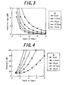
  • Figure 3 is a diagram showing the relation between the branch angle ⁇ of the cross waveguide and the loss
  • Figure 4 is a diagram showing the relation between the branch angle ⁇ of the cross waveguide and the crosstalk.
  • the relations when each of the spot size of the light propagating through the cross waveguide is set at 5 ⁇ m, 7.5 ⁇ m, 10 ⁇ m, 12.5 ⁇ m, and 15 ⁇ m are plotted, and the propagating light is assumed to be circular.
  • the analysis is performed under the assumption that the distribution of the intensity of the light waves propagating through the cross waveguide is a Gaussian distribution.
  • the light waves in the optical input waveguide and the optical output guide each having a normal optional confinement effect are in the shape of the Gaussian distribution.
  • the branch angle ⁇ is, the larger the size of the cross waveguide 22 at the longitudinal direction in Figure 2A is, as a result, the optical loss and the crosstalk increase.
  • the size and the material of the waveguide are selected so that the spot size of the light propagating through the waveguide of the optical switch is about 5 ⁇ m so as to be substantially equal to that of the light propagating through the single-mode optical fiber or is less than 5 ⁇ m by making the optical confinement stronger.
  • the present embodiment it is possible to reduce the loss and the crosstalk without the increase of the optical device size by having the spot size of the light propagating through the cross waveguide 22 larger than that of light propagating through the optical input waveguides 21a and 21b, the optical output waveguides 23a and 23b, or the connection waveguides 24a, 24b, 25a and 25b, as a result, the operating efficiency of the optical device can be improved.
  • ⁇ T is a rough estimate of the amount of temperature change required for the amount of refractive index change ⁇ nc in case of using polymer as the material of the waveguide and considering a TO effect of the polymer (-1 x 10 -4 /°C ⁇ ⁇ nc ⁇ -2 x 10 -4 /°C).
  • ⁇ nc(%) 0.1 0.2 0.3 0.4 0.5 ⁇ T(°) 10 20 30 40 50 ⁇ c(°) 2.6 3.6 4.4 5.1 5.7
  • Figure 6A is a diagram showing the relation between the waveguide size and the coupling loss with the optical fiber when the thickness of the core layer with the waveguide is 6 ⁇ m
  • Figure 6B is a diagram showing the relation between the waveguide size and the coupling loss with the optical fiber when the thickness of the core layer with the waveguide is 2 ⁇ m.
  • the optical confinement is weakened and thus the spot size decrease as the width reduces. Therefore, if the coupling loss is small, the spot size wf is substantially realized by the waveguide size of itself.
  • the light propagating through the waveguide with the width W and the thickness T different from each other generally has a shape similar to an ellipse. Assuming that the spot size in the lateral direction is wx and that in the vertical direction is wy, an effective spot size is represented by (wx x wy) 1/2 .
  • the spot size wf can be set at a proper size by changing the width W.
  • the width W is 7 ⁇ m when the thickness T is 6 ⁇ m, and the width W is 8-10 ⁇ m when the thickness T is 2 ⁇ m.
  • the width W is 2 ⁇ m when the thickness T is 6 ⁇ m, and the width W is 4-4.5 ⁇ m when the thickness T is 2 ⁇ m. Therefore, the spot size wf can be set at a desired size by selecting the material of the waveguide, the refractive index difference ⁇ n, the thickness T or the width W properly.
  • the tapered waveguides 28a, 28b, 29a and 29b gradually varying in width or thickness are formed and the taper length of theirself is set at a degree of several 10 ⁇ m to several 100 ⁇ m for example, and thereby the coupling loss between the waveguides can be reduced.
  • the spot size as desired by having the cross waveguide with the same size as that of the waveguides in the other area and having the refractive index differences in the respective areasdifferent from one another.
  • the refractive index differences among the tapered waveguides 28a, 28b, 29a and 29b vary gradually.
  • the present embodiment it is possible to reduce the optical loss and the crosstalk in the optical device and improve the operating efficiency of the optical device by making the spot size of the light propagating through the cross waveguide larger than that of the light propagating through the optical input waveguide, the optical output waveguide or the connection waveguide.
  • any other waveguide than the cross waveguide is formed so that the radiation loss is small by making the optical confinement strong and thus making the spot size of the light small.
  • FIG. 7 is a diagram showing a second embodiment of the optical device according to the present invention.
  • This optical device comprises optical input waveguides 171a and 171b and optical output waveguides 172a and 172b each having the width W1 and the thickness T1, curved waveguides 173a, 173b, 174a and 174b each having the width W2 and the thickness T2, and a cross waveguide 175 having the width W3 and the thickness T3 as a core layer.
  • it has relations of "W3 ⁇ W1" and "T1 ⁇ T3".
  • Tapered waveguides 176, 177, 178 and 179 interposed between the curved waveguides 173a, 173b, 174a and 174b and the cross waveguide 175 have tapered portions 176a, 177a, 178a and 179a extending from the curved waveguides 173a, 173b, 174a and 174b, and tapered portions 176b, 177b, 178b and 179b extending from the cross waveguide 175.
  • the spot size of the light is converted with a low loss by each of these tapered portions 176a, 177a, 178a and 179a and tapered portions 176b, 177b, 178b and 179b.
  • these waveguides of the single core layer by forming the lateral width and the layer thickness of them into a tapered shape.
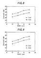
  • Figure 8 is a diagram showing the relation between the width of a core layer with the thickness of 1 ⁇ m or 2 ⁇ m and the crosstalk of the second embodiment
  • Figure 9 is a diagram showing the relation between the width of a core layer with the thickness of 2 ⁇ m or 4 ⁇ m and the crosstalk of the second embodiment.
  • the branch angle ⁇ is 4° and the refractive index difference between the core layer and the clad layer is 0.5%
  • the branch angle ⁇ is 4° and the refractive index difference between the core layer and the clad layer is 0.3%.
  • the branch/cross waveguide is of a single-mode waveguide structure.
  • the second embodiment it is possible to realize a crosstalk reduction effect being remarkably excellent in comparison with a conventional waveguide structure by making a structure having the optical confinement effect in the waveguide with the core layer much thinner than the ordinary waveguide structure.
  • a principle for obtaining such an effect is described in the following.
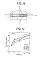
  • Figure 10 shows the distribution of the intensity of light waves propagating through a branch/cross waveguide in a section of the waveguide.
  • the distribution of the intensity in the lateral direction (x direction) of a core layer c is nearly in the shape of a Gaussian distribution.
  • the distribution of the intensity in the vertical direction (y direction) of the core layer c takes the shape of an exponential distribution different from the ordinary waveguide. This is caused by a fact that the spot size of the light waves in the vertical direction is substantially larger than the thickness T of the core layer c due to a small optical confinement effect in the waveguide in the vertical direction.
  • Figures 11 to 13 show the relation between the crosstalk and the branch/cross angle ⁇ in case of setting the thickness of the core layer c at 4 ⁇ m, 3 ⁇ m and 2 ⁇ m when the refractive index difference between the core layer and the clad layer is 0.2% in the present invention, respectively.
  • Figure 11 shows a characteristic in case of forming a waveguide having a comparatively intense optical confinement effect by making the thickness T of a core layer c comparatively large.
  • Figure 11 like the characteristic shown in Figure 4, as large the branch/cross angle ⁇ and the width W of the core layer c are, the greater the crosstalk characteristic.
  • Figure 11 is different from Figure 4 in that the effect of improvement in the crosstalk is not remarkable even if the branch/cross angle ⁇ is comparatively large.
  • the branch/cross angle ⁇ is larger than 6°, the crosstalk characteristic tends to be worse.
  • the light waves propagating through the core layer c have the distribution of the intensity in the shape of the exponential distribution as shown in Figure 10.
  • Such light waves in the shape of the exponential distribution have a substantially small spot size in the central part (core part) of the optical waveguide, namely, they have properties obtained by superposing the light waves being effectively intense in the optical confinement on light waves being comparatively larger in the spot size in the periphery (clad part) of the optical waveguide.
  • the optimum cross/branch angle ⁇ with a good crosstalk in a range of comparatively small angles.
  • the optimum cross/branch angle ⁇ depends on the material, the refractive index difference and the structure of the optical waveguide.
  • the crosstalk characteristic tends to be improved as the cross/branch angle ⁇ increases similar to the construction of the optical waveguide throught which the light waves in the shape of a normal Gaussian distribution propagate.
  • Figures 8 and 9 have respectively shown the cases that the refractive index difference between the core layer and the clad layer is 0.5% and 0.3%, respectively, however, in case that the refractive index of the core layer is different from that of the clad layer, an effect of the present invention can be obtained by properly setting the width and the thickness of the core layer according to the refractive index difference between these layers.
  • Figure 14A is a top view of a third embodiment of the optical device according to the present invention, and Figure 14B shows a section III-III of Figure 14A.
  • This embodiment takes a 2 x 2 switch form by arranging an electrode 42 just above the cross part of a cross waveguide 41.
  • the present invention can be also applied to such an optical switch of the 2 x 2 switch form.
  • Figure 15 is a diagram showing a fourth embodiment of the optical device according to the present invention. This has a 2 x 2 switch form with a cross waveguide 51 and four electrodes 44a, 44b, 44c and 44d, and the present invention can be also applied to this.
  • Figure 16 is a diagram showing a fifth embodiment of the optical device according to the present invention.
  • This forms a matrix switch, and comprises core layers 51 with optical waveguides, a clad layer 52, optical fibers 53 connected to the input side and output side, cross waveguides 54 and optical switch elements 55.
  • a cross waveguide structure of the above-mentioned optical switch portion may be used as the cross waveguide 54, and any of the first type of the switch and the second type of the switch may be used as the optical switch element 55. In this case it is possible to realize an optical switch matrix to which the present invention is applied.
  • the single-mode optical waveguide is used as the optical waveguide
  • the present invention when using the waveguide with a small length or that formed with a high accuracy waveguide processing technique, it is possible to apply the present invention because a low mode conversion loss can be achieved even if the multi-mode optical waveguide is used as a part of the optical device.
  • the present invention can be applied to the case of using the multi-mode optical waveguide as the whole optical waveguides.
  • the above-mentioned embodiments can be applied to all optical devices such as a semiconductor optical waveguide device utilizing a plasma effect caused by carriers in a semiconductor, a multiple quantum well structure effect and the like, and a ferroelectric optical waveguide device composed of lithium niobate or the like utilizing an EO effect, and they are each formed of an optical device composed of glass, polymer and the like utilizing a TO effect as the most suitable ones.
  • Figure 17 is a diagram showing a sixth embodiment of the optical device according to the present invention.
  • This shows a section of the central part of a cross waveguide, and comprises a core layer 101 of the refractive index n having an optical waveguide, a first clad layer 102 of refractive index ns1 and the thickness ts1, a second clad layer 103 of the refractive index ns2 and the thickness ts2, an electrode 104 for changing the refractive index of the cross waveguide by applying a certain voltage or supplying a certain current, and a substrate 105.
  • the core layer 101, the clad layer 102 and the clad layer 103 are each formed of a polymer material such as polyimide with a negative temperature coefficient, and the relation among the refractive indexes is: nc>ns2>ns1.
  • Figure 18 is a diagram showing an effective temperature distribution at a vicinity of a cross waveguide of the conventional optical device in which the first clad layer has the same refractive index as that of the second clad layer
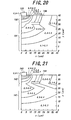
  • Figures 19 to 21 are diagrams each showing an effective temperature distribution at a vicinity of a cross waveguide of an optical device according to the present invention in which the refractive index of the first clad layer is different from that of the second clad layer.
  • These temperature distributions represent values calculated by the finite element method, and the numerical ranges in the figures represent respectively values normalized by the temperature of the electrodes 113, 123, 133 and 143 taking the temperature of a substrate not shown in figures as a reference value.
  • the thicknesses of the first clad layers 111, 121, 131 and 141 are respectively 30 ⁇ m, and the thicknesses of the second clad layers 112, 122, 132 and 142 are respectively 10 ⁇ m.
  • the first clad layers 111, 121, 131 and 141, the second clad layers 112, 122, 132 and 142, and the core layers 114, 124, 134 and 144 are each composed of the polyimide material.
  • the polyimide material has a TO effect in which the refractive index decreases as the temperature increases. Therefore, these temperature distributions correspond to the spatial distributions of the refractive index change portions based on the TO effect, and shows that the refractive index decreases as the temperature increases.
  • the center of the core layer 114 at a position being about 10 ⁇ m in depth from the surface of the second clad layer 112 and about 10 to 20 ⁇ m apart in the x-axis direction from an end of the electrode 113.
  • a part of the reflection light is radiated due to a fact that an isothermal line of the temperature distribution is inclined to a y-z axis plane, namely, a plane perpendicular to the x-axis at a vicinity of the core layer 114, and the total reflection surface of light input into the cross waveguide is deviated from the plane perpendicular to the x-axis.
  • the first clad layers 121, 131 and 141 have a lower refractive index than that of the second clad layers 122, 132 and 142.
  • the difference in the refractive index between the first clad layers 121, 131 and 141 and the second clad layers 122, 132 and 142 is 0.05%
  • the refractive index difference is 0.1%
  • the refractive index difference is 0.2%.
  • the first clad layers 121, 131 and 141 are larger by 0.01 in terms of normalized temperature per refractive index difference of 0.01%.
  • Figures 16 to 18 shows the result of calculation of an effective temperature distribution obtained by considering such an effect. That is to say, when the refractive index difference is set at about 0.05% to 0.1%, the temperature distribution (isothermal line) at a vicinity of the core layer is substantially perpendicular to the x-axis.
  • the loss and the crosstalk caused by the total reflection of the light can be reduced by considering the influence of the TO effect or the EO effect of the waveguide material and the position of a core layer, and properly setting the thickness and the refractive index difference of the clad layer.
  • magnitude of the refractive index can be set by a proper combination of ingredients and the like
  • the thickness can be set by adjusting the viscosity of an unhardened polymer material or the rotation speed of a spinner, and these waveguide structures can be realized by using a conventional photolithographic technique or film forming technique.
  • Figure 22 is a diagram showing a seventh embodiment of the optical device according to the present invention.
  • This shows a section of the central part of a cross waveguide, and comprises a core layer 151 of the refractive index nc having the optical waveguide, a first clad layer 152 of the refractive index ns11 and the thickness ts11, a second clad layer 153 of the refractive index ns1 and the thickness ts12, a third clad layer 154 of the refractive index ns13 and the thickness ts13, an electrode 155 for changing the refractive index of the cross waveguide by applying a certain voltage or supplying a certain current, and a substrate 156.
  • the core layer 151, the clad layer 152, the clad layer 153 and the clad layer 154 are each composed of the polymer material such as the polyimide with the negative temperature coefficient, and the relation among the refractive indexes is: nc > ns12 > ns11 > ns13.
  • the present invention can be also applied to a case of further comprising the third clad layer 154 in this way.
  • Two or more clad layers may be interposed between the second clad layer and the substrate.
  • Figure 23A is a top view of an eighth embodiment of the optical device according to the present invention, and Figure 23B shows a section IV-IV of Figure 23A.
  • two electrodes 162 and 163 are arranged above a branch waveguide 161.
  • the present invention can be also applied to this case.
  • the refractive indexes need to have the following relation: ns2 ⁇ ns1
  • the refractive indexes need to have the following relation: ns12 ⁇ ns11 ⁇ ns13.
  • a current injection effect of a semiconductor to the distribution of the intensity of the electric field formed by an applied voltage between the electrode and the substrate and set the refractive index and the thickness of the clad layer, and the principle of the present invention can be also applied to any optical material.
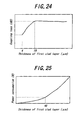
  • the thickness of the first clad layer is smaller than 15 ⁇ m, the coupling loss decreases.
  • the thickness of the first clad layer is smaller than 4 ⁇ m, however, the light may leak from the first clad layer, and thus the propagation loss may degrade. As a result, it is preferable to have the thickness of the first clad layer not less than 4 ⁇ m.
  • the thickness of the first clad layer is not less than 15 ⁇ m, the coupling loss is substantially saturated and a substantial reduction of the coupling loss is not achieved. And as shown in Figure 25, when the thickness of the first clad layer exceeds 40 ⁇ m, the rate of the increase of the power supply is remarkable. As a result, the thickness of the first clad layer is preferably not more than 40 ⁇ m, and more preferably, it is not more than 15 ⁇ m.
  • a conventional 2 x 2 optical device uses a waveguide whose core layer has a comparatively large sectional area and which has a remarkably intense optical confinement effect, it is necessary to have a comparatively narrow width t of an electrode 272 arranged in the central part near the branch waveguide, namely, the ratio (t/d) of the width t of the electrode 272 to the width d of the waveguide in Figure 26 in order to have the excessive loss as small as possible.
  • the width t is small, however, it is difficult to align the electrode 272 with the branch waveguide 271, and making an electric current flow through the electrode 272 is liable to cause the breaking of wire.
  • the width t of the electrode 274 arranged near the branch waveguide 273 shown in Figure 27, namely, the ratio (t/d) of the width t to the width d of the waveguide is comparatively large, and thus an optical switching is performed in such a manner that the light passes through the first clad layer 275 from the branch optical waveguide 273 and propagates again through the branch waveguide 273 as shown by an arrow.
  • Figure 28 shows the relation between the loss in the switching operation (the reflection loss) and a standard value t/d of the electrode width in the 2 x 2 optical devices of the prior art and the present invention.
  • the shape of a core (T/d, T: core thickness) is taken as a parameter. It is found from Figure 28 that in the optical device using a conventional optical waveguide with an intense optical confinement, if t/d is very small, the loss is small, however, the loss increases remarkably as the t/d increases. In this phenomenon, the electrode end parts 272-1 and 272-2 function as the total reflection surfaces to the wave-guided light in the switching operation, and as t/d increases, the reflected light leaks to the clad and causes a substantial loss.
  • the present invention when t/d is small, a slight excess loss occurs in the switching operation. This is caused by the loss occurring at the branch/cross part because of using the single-mode waveguide with a weak confinement. However, it is possible to suppress the loss to a slight increase though t/d increases. The reason is that in the present invention as the third clad layer 154 having a relatively small refractive index as shown in Figure 22 is arranged, the reflected light leaking to the clad region 275 is coupled again into the branch waveguide 273 and the increase of loss is suppressed. Therefore, if t/d is not less than 0.2, the reflection loss can be greatly reduced in comparison with the prior art.
  • the width t of the electrode 274 is larger than a value in a certain range, there is a problem that the power consumption of the electrode increases. Also, when the width of a region functioning as the core layer increases and the light reaches the output side of the waveguide, evanescent waves at the region functioning as the core layer leak to the output side of the waveguide and the extinction ratio decreases. Therefore, the optimum range of the width t of the electrode 274 depends on the thickness of the clad layer and the width d of the core layer, and the maximum extinction ratio is obtained by making the width t not more than 3 times the width d of the core layer 271.
  • the present invention can be also applied to an optical device having a single input waveguide, not less than three output waveguides and a branch waveguide for connecting them, an optical device having not less than three input waveguides, a single output waveguide and a branch waveguide for connecting them, an optical device having not less than two input waveguides, not less than three output waveguides and a cross waveguide for connecting them, or an optical device having not less than three input waveguides, not less than two output waveguides and a cross waveguide for connecting them.
  • an optical device provided with an optical switch has been described, however, the present invention can be also applied to an optical device without an optical switch.
  • the spot size of the light propagating through the branch/cross waveguide is larger than that of the light propagating through the optical input waveguide, the optical output waveguide or the connection waveguide has been described, however, when the spot size of the light propagating through the branch/cross waveguide is not less than 5 ⁇ m, it is possible to have a small loss of the optical input waveguide, the optical output waveguide or the connection waveguide and have a small diffraction of the light at the branch/cross waveguide regardless of the spot size of the light propagating through the optical input waveguide, the optical output waveguide or the connection waveguide, and thus it is possible to reduce the optical loss and crosstalk in the optical device.
  • Such an optical device can be formed by coupling light input into the optical input waveguide with a lens or a spot magnifying waveguide and coupling light output from the optical output waveguide with the lens or the spot magnifying waveguide in the optical switch in Figure 1, for example.
  • the spot size of each light propagating through the branch/cross waveguide, the optical input waveguide, the optical output waveguide and the connection waveguide is not less than 5 ⁇ m.

Landscapes

  • Physics & Mathematics (AREA)
  • General Physics & Mathematics (AREA)
  • Optics & Photonics (AREA)
  • Engineering & Computer Science (AREA)
  • Nonlinear Science (AREA)
  • Microelectronics & Electronic Packaging (AREA)
  • Power Engineering (AREA)
  • Optical Integrated Circuits (AREA)

Abstract

The spot size of light propagating through a cross waveguide 22 is larger than the spot size of light propagating through optical input waveguides 21a and 21b, optical output waveguides 23a and 23b, or connection waveguides 24a, 24b, 25a and 25b.

Description

TECHNICAL FIELD
The present invention relates to an optical device included in a photonic network utilizing a wavelength division multiplex (WDM) method, for example.
BACKGROUND ART
With the development of the photonic network and optical switching technology, an optical device, for example, an optical switch using an optical waveguide, an optical waveguide device such as an optical modulator and so on tends to be often used.
For example, an optical switch includes a first type using a directional coupler or a Mach-Zender interference waveguide and a second type using a branch/cross waveguide.
The first type of the optical switch operates analogically, for example, as the voltage to be applied for its switching operation increases, the intensity of the output light from the switch gradually reduces to around zero, after then as the voltage increases furthermore, the intensity increases again. On the other hand, the second type of the optical switch operates digitally in general, and performs an on-off operation by applying the voltage not less than a certain value.
The first type of the optical switch performs an on-off operation by changing the phase of light waves propagating in a waveguide. Therefore, for example, as the first type of the optical switch can perform the switching operation only by slightly changing the refractive index of a waveguide with an electro-optical effect, the first type of the optical switch has an advantage to make the operating voltage of the first type of the optical switch small and have a comparatively high operation efficiency.
However, the first type of the optical switch has a disadvantage to have a comparative large size of necessity. Also, in order to perform the on-off operation, it is necessary to set the operating voltage of the first type of the optical switch at an appropriate value according to the switching characteristic of the first type of the optical switch. As a result, an electronic circuit for controlling the optical switch has a complex construction, particularly, in case of a device having a plurality of switch elements such as a matrix switch, it is necessary to perform a fine adjustment of the voltage to each switch.
On the other hand, the second type of the optical switch has an advantage to have a comparative small size. As it is enough to apply the voltage not less than a certain value in order to perform the switching operation, the second type of the optical switch has an advantage to omit an electric circuit for control and to control easily compared with the first type of the optical switch.
Figure 1A is a top view of such a first type of the optical device, Figure 1B is a diagram showing a section I-I of Figure 1A, and Figure 1C is a diagram showing a part surrounded by a dashed line in Figure 1A. This optical device includes a core layer 1 with a cross waveguide, a clad layer 2, an electrode 3 disposed on the cross waveguide and a substrate 4, with the clad layer 2 being deposited on the substrate 4.
This optical device utilizes the total reflection phenomenon of light in the switching operation. That is, when a certain voltage is applied to or a certain current is supplied to the electrode 3, the refractive index of a waveguide just under the electrode 3 is changed by an electro-optical (EO) effect or a thermo-optical (TO) effect of a material composing the waveguide.
Due to such an operation, an input light P0 to the waveguide goes straight in the waveguide to become an output light P1, or is totally reflected by the surface just under the electrode 3 to become an output light P2.
In case of such a second type of the optical device, however, in order to generate the variation in refractive index necessary to occur the total reflection, it is necessary to make the operating voltage of the second type of the optical switch larger than the first type of the optical device.
In this case, as it is possible to make the amount of variation in refractive index necessary to occur the total reflection small by making the branch angle  of the cross waveguide, the efficiency of the switching operation can be improved. However, as the smaller the branch angle , the larger the size of the optical device, and thus there is a disadvantage to increase the loss and crosstalk remarkably.
As a measure to counter this, as described in Electronics Letters, Vol. 25, No. 11, pp.730-731, 1989, a method of suppressing crosstalk by making the core layer of a branch/cross waveguide wider in width than the core layers of an optical input waveguide and an optical output waveguide is used.
In this case, as the branch/cross waveguide has a comparative large sectional area, the optical confinement effect in the waveguide is remarkable strong, and thus so-called a multi-mode waveguide performing the propagation in a plurality of modes is formed.
For the purpose of this, because of a slight variation in shape and material of the waveguide of a product, a basic-mode light input from the optical input waveguide is converted into a high-order mode light result from the propagation through this branch/cross waveguide.
The radiation loss or coupling loss to the optical output waveguide caused by such a conversion increases, and thus the optical device may have a remarkable large loss.
Moreover, in case of changing the refractive index of the waveguide with the thermo-optical effect, the amount of variation in refractive index is in proportion to the distribution of the temperature so that the electrode 3 has the highest temperature. Therefore, as the total reflection surface of light formed by changing the refractive index of the waveguide is the same in shape as this distribution of the temperature, and is not perpendicular but inclined to the surface of the clad layer 2, a part of the light reflected by the total reflection surface is emitted from the waveguide, and thus the loss increases. Also, such a part of light may couple to the optical output waveguide opposite to the optical input waveguide, and the crosstalk may degrade.
The object of the present invention is to provide an optical device capable of reducing the optical loss and the crosstalk as well as improving the operating efficiency.
DISCLOSURE OF THE INVENTION
According to the present invention, there is provided an optical device comprising;
  • an optical input waveguide,
  • a branch/cross waveguide,
  • an optical output waveguide, and
  • connection waveguides for respectively connecting said optical input waveguide and the branch/cross waveguide and connecting the optical output waveguide and the branch/cross waveguide to each other,
  •    wherein the spot size of light propagating through the branch/cross waveguide is larger than the spot size of light propagating through the optical input waveguide, the optical output waveguide, or the connection waveguide.
    In the optical input waveguide, the optical output waveguide or the connection waveguide, the coupling loss with the optical element or the optical waveguide to be connected to the optical input waveguide and the radiation loss in the connection waveguide reduce in accordance with the reduction of the spot size of a light due to the increasing of the optical confinement.
    On the other hand, in a branch/cross waveguide, the diffraction of the light, therefore, the loss and the crosstalk reduce as the spot size of light increases.
    According to the present invention, as the spot size of the light propagating through the branch/cross waveguide larger than that of the light propagating the optical input waveguide, the optical output waveguide or the connection waveguide makes the optical confinement strong and makes the diffraction of the light small, the optical loss and the crosstalk of the optical device reduce. From a viewpoint of the operating efficiency, it is preferable to make a branch angle small, however, according to the present invention, it is possible to improve the operating efficiency of the optical device because it is possible to have a relative small branch angle without affecting the optical loss and the crosstalk by having a relative large spot size of the light propagating through the branch/cross waveguide.
    In this specification, the branch/cross waveguide means a branch waveguide or a cross waveguide.
    In order to reduce the optical loss and the crosstalk, the spot size of light propagating through the branch/cross waveguide is preferably not less than 5µm, and the spot size of the light propagating through the optical input waveguide, the optical output waveguide or the connection waveguide is preferably less than 5µm.
    Another optical device according to the present invention comprises;
  • an optical input waveguide,
  • a branch/cross waveguide,
  • an optical output waveguide, and
  • connection waveguides for respectively connecting the optical input waveguide and the branch/cross waveguide and connecting the optical output waveguide and the branch/cross waveguide to each other,
  •    wherein the spot size of light propagating through said branch/cross waveguide is not less than 5µm.
    With the spot size of the light propagating through a branch/cross waveguide not less than 5µm in the present invention, it is possible to make the optical confinement in the optical input waveguide, the branch/cross optical waveguide or the connection waveguide strong and make the diffraction of the light in the branch/cross optical waveguide small, and thus the optical loss and the crosstalk of the optical device reduce regardless of the spot size of the light propagating through the optical input waveguide, the optical output waveguide or the connection waveguide.
    In order to achieve the effect of a remarkable crosstalk reduction, it is preferable to set at least one of the width and the thickness of said branch/cross waveguide at a value smaller than the width or the thickness of the optical input waveguide and the optical output waveguide, and/or to set the ratio of width to the thickness of the branch/cross waveguide not less than 10/4.
    Another optical device of the present invention comprises;
  • an optical input waveguide,
  • a branch/cross waveguide,
  • an optical output waveguide, and
  • connection waveguides for respectively connecting the optical input waveguide and the branch/cross waveguide and connecting the optical output waveguide and the branch/cross waveguide to each other,
  •    wherein at least one of the width and thickness of said branch/cross waveguide is set at a value smaller than the width or the thickness of the optical input waveguide and the optical output waveguide.
    Another optical device of the present invention comprises;
  • an optical input waveguide,
  • a branch/cross waveguide,
  • an optical output waveguide, and
  • connection waveguides respectively for connecting the optical input waveguide and the branch/cross waveguide and connecting the optical output waveguide and the branch/cross waveguide to each other,
  •    wherein the ratio of the width to the thickness of the branch/cross.waveguide is not less than 10/4.
    Preferably, the width and the thickness of the branch/cross waveguide are not less than 10µm and not more than 4µm, respectively, and more preferably, the cross/branch angle of the branch/cross waveguide is 3 to 6 degrees. The branch/cross waveguide consists of a single-mode waveguide, for example.
    Preferably, the branch/cross waveguide has a tapered waveguide. Thereby, as it is possible to gradually change the spot size between waveguides different in spot size from each other, the optical loss can be reduced.
    Preferably, it is possible to reduce the coupling loss between the optical input waveguide and the optical device such as a plane light circuit (PLC) and a semiconductor optical device or the optical waveguide such as an optical fiber by the spot size of the light input into the optical input waveguide substantially equal to the spot size of the light output from an optical element or an optical waveguide to be connected to the optical input waveguide.
    If the spot size of the light output from the optical output waveguide is substantially equal to the spot size of the light input into the optical element or the optical waveguide to be connected to the optical output waveguide, it is possible to reduce the coupling loss between the optical output waveguide and the optical device or the optical waveguide.
    The device of the present invention may further comprise an optical switch for switching over the direction of propagation of light input into the branch/cross waveguide, in this case, the optical switch hsa at least one electrode for changing the refractive index of the branch/cross waveguide by applying a certain voltage or supplying a certain current, for example.
    Another optical device according to the present invention comprises;
  • a core layer having a branch/cross waveguide,
  • a first clad layer having a specific refractive index, with the core layer being deposited on a part of a surface of the first clad layer,
  • a second clad layer having a refractive index different from that of the first clad layer, with the core layer being provided between the first clad layer and the second clad layer, and
  • at least one electrode for changing the refractive index of the branch/cross waveguide by applying a certain voltage or supplying a certain current.
  • According to the present invention, as the second clad layer having a refractive index different from that of the first clad layer, the total reflection surface may be substantially perpendicular to the surface of the second clad layer. As a result, the loss reduces because the light reflected by the total reflection surface does not substantially emit from a waveguide. Also, the degradation of the crosstalk result from the coupling of a part of the light into the optical output waveguide opposite to the optical input waveguide.
    From a viewpoint of reduction of the coupling loss, the thickness of the first clad layer is preferably between 4µm and 40µm, and more preferably between 4µm and 15µm.
    A core layer with a single-mode optical waveguide does not have a remarkable strong optical confinement effect because of a comparative small sectional area of the core layer, and is generally called a flat core layer.
    The core layer may have a single-mode optical input waveguide, a single-mode branch/cross waveguide and a single-mode optical output waveguide,
  • the electrode may be a rectangular electrode disposed near the single-mode branch/cross waveguide,
  • the ratio of the width of the electrode to that of said waveguide may be not less than 0.2 and/or not more than 3, so that the optical device has a function of switching the light so as to pass through the first clad layer from the single-mode branch/cross waveguide and propagate again through the single-mode branch/cross waveguide.
  • In this case, even if the ratio of the width of the electrode to that of the optical waveguide is relatively large, it is possible to have a substantially small excess loss and to have a relatively large extinction ratio of the switching because the optical confinement is not remarkably strong. The ratio of the width of the electrode to that of the optical waveguide is established by the relation between the temperature of the electrode and the driving power.
    For example, each of the first clad layer and the second clad layer consists of a material having a negative temperature coefficient, and the refractive index of the first clad layer is lower than that of the second clad layer.
    Alternatively, each of the first clad layer and the second clad layer consists of a material having a positive temperature coefficient, and the refractive index of the first clad layer is higher than that of the second clad layer.
    BRIEF DESCRIPTION OF THE DRAWINGS
  • Figure 1 is a diagram showing a conventional optical switch.
  • Figure 2 is a diagram showing a first embodiment of the optical device according to the present invention.
  • Figure 3 is a diagram showing the relation between the branch angle  and loss of the cross waveguide.
  • Figure 4 is a diagram showing the relation between the branch angle  and crosstalk of the cross waveguide.
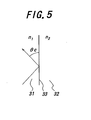
  • Figure 5 is a diagram showing the principle of the present invention.
  • Figure 6 is a diagram showing the relation between the size of the waveguide and the coupling loss with the optical fiber.
  • Figure 7 is a diagram showing a second embodiment of the optical device according to the present invention.
  • Figure 8 is a diagram showing the relation between the width of a core layer with the thickness of 1µm or 2µm and the crosstalk of the second embodiment.
  • Figure 9 is a diagram showing the relation between the width of a core layer with the thickness of 2µm or 4µm and the crosstalk of the second embodiment.
  • Figure 10 is a diagram showing the distribution of the light intensity in the branch/cross waveguide of the second embodiment of the optical device according to the present invention.
  • Figure 11 is a diagram showing the relation between the branch angle  and the crosstalk in the cross waveguide when the thickness of the core layer is 4µm.
  • Figure 12 is a diagram showing the relation between the branch angle  and the crosstalk in the cross waveguide when the thickness of the core layer is 3µm.
  • Figure 13 is a diagram showing the relation between the branch angle  and the crosstalk in the cross waveguide when the thickness of the core layer is 2µm.
  • Figure 14 is a diagram showing a third embodiment of the optical device according to the present invention.
  • Figure 15 is a diagram showing a fourth embodiment of the optical device according to the present invention.
  • Figure 16 is a diagram showing a fifth embodiment of the optical device according to the present invention.
  • Figure 17 is a diagram showing a sixth embodiment of the optical device according to the present invention.
  • Figure 18 is a diagram showing the distribution of the temperature of the optical device of the prior art.
  • Figure 19 is a diagram showing the distribution of the temperature of the optical device of 0.05% in refractive index difference according to the present invention.
  • Figure 20 is a diagram showing the distribution of the temperature of the optical device of 0.10% in refractive index difference according to the present invention.
  • Figure 21 is a diagram showing the distribution of the temperature of the optical device of 0.20% in refractive index difference according to the present invention.
  • Figure 22 is a diagram showing a seventh embodiment of the optical device according to the present invention.
  • Figure 23 is a diagram showing an eighth embodiment of the optical device according to the present invention.
  • Figure 24 is a diagram showing the relation between the thickness of the first clad layer and the coupling loss.
  • Figure 25 is a diagram showing the relation between the thickness of the first clad layer and the power consumption.
  • Figure 26 is a diagram for explaining the relation between the width of the electrode and that of the optical waveguide in the optical device of the prior art.
  • Figure 27 is a diagram for explaining the relation between the width of the electrode and that of the optical waveguide in the optical device according to the present invention.
  • Figure 28 is a diagram for explaining the relation among the ratio of the width of the electrode to that of the optical waveguide, the temperature of the electrode and the driving power in the optical device according to the present invention.
  • BEST MODE FOR CARRYING OUT THE INVENTION
    Embodiments of the optical device according to the present invention are described in detail with reference to the drawings. In embodiments described below, the optical device using a flat core as the core layer is described, but the optical device is not limited to this as long as it is not described in particular.
    Figure 2A is a top view of a first embodiment of the optical device according to the present invention, and Figure 2B shows a section II-II of Figure 2A.
    This optical device formed as a 1 x 2 optical switch includes a core layer 11, a clad layer 12, an electrode 13 disposed on a cross waveguide and a substrate 14, with the clad layer 12 being deposited on the substrate 14.
    The core layer 11 has optical input waveguides 21a and 21b, a cross waveguide 22, optical output waveguides 23a and 23b, connection waveguides 24a and 24b respectively for connecting the optical input waveguide 21a and the cross waveguide 22 and connecting the optical input waveguide 21b and the cross waveguide 22, and connection waveguides 25a and 25b respectively for connecting the optical output waveguide 23a and the cross waveguide 22 and connecting the optical output waveguide 23b and the cross waveguide 22. The connection waveguides 24a, 24b, 25a and 25b have curved waveguides 26a, 26b, 27a and 27b, and tapered waveguides 28a, 28b 29a and 29b, respectively. Each of these optical input waveguides 21a and 21b, cross waveguide 22, optical output waveguides 23a and 23b, and connection waveguides 24a, 24b, 25a and 25b is a single-mode optical waveguide.
    In this embodiment, the width of the cross waveguide 22 is smaller than those of the optical input waveguides 21a and 21b, the optical output waveguides 23a and 23b, and the curved waveguides 26a, 26b, 27a and 27b. Also, the spot size of the light propagating through the cross waveguide 22 is larger than that of the light propagating through the optical input waveguides 21a and 21b, the optical output waveguides 23a and 23b, or the connection waveguides 24a, 24b, 25a and 25b.
    Figure 3 is a diagram showing the relation between the branch angle  of the cross waveguide and the loss, and Figure 4 is a diagram showing the relation between the branch angle  of the cross waveguide and the crosstalk. In Figures 3 and 4, the relations when each of the spot size of the light propagating through the cross waveguide is set at 5µm, 7.5µm, 10µm, 12.5µm, and 15µm are plotted, and the propagating light is assumed to be circular.
    And in order to simplify the calculation, the analysis is performed under the assumption that the distribution of the intensity of the light waves propagating through the cross waveguide is a Gaussian distribution. The light waves in the optical input waveguide and the optical output guide each having a normal optional confinement effect are in the shape of the Gaussian distribution.
    In the switching state where the light is input into the optical input waveguide 21a and is output from the optical output waveguide 23b, if the optical power of the input light is represented as P10, that of the light output from the optical output waveguide 23b is represented as P11, and that of the light output from the optical output waveguide 23a is represented as P12, the loss is represented by P11/P10 and the crosstalk is represented by P12/P10.
    Because the light input into the cross waveguide 22 travels and spreads due to the influence of the diffraction, the loss and the crosstalk of the light occur at the output side of the cross waveguide 22 in principle. Therefore, the smaller the branch angle  is, the larger the size of the cross waveguide 22 at the longitudinal direction in Figure 2A is, as a result, the optical loss and the crosstalk increase.
    In case of the single-mode optical waveguide, as the spot size of the light decreases by the strong optical confinement, the radiation loss of the light at the curved waveguide decreases. In case of a conventional optical switch, it is possible to reduce the coupling loss with an optical fiber to be connected to the switch and the radiation loss at the curved waveguide.
    In the conventional optical switch, in order to reduce the coupling loss and the radiation, the size and the material of the waveguide are selected so that the spot size of the light propagating through the waveguide of the optical switch is about 5µm so as to be substantially equal to that of the light propagating through the single-mode optical fiber or is less than 5µm by making the optical confinement stronger.
    As seen from Figures 3 and 4, in order to reduce the loss to 1 dB or less and obtain the crosstalk to 50 dB or more, not less than 8° of the branch angle  is required. If the branch angle  is constant, as the spot size increases, the reduction of the loss and the improvement of the crosstalk increase. Further, if the loss and the crosstalk are constant, respectively, as the spot size increases, the branch angle  increases because as the spot size increases, the diffraction of the light at the cross waveguide reduces.
    According to the present embodiment, it is possible to reduce the loss and the crosstalk without the increase of the optical device size by having the spot size of the light propagating through the cross waveguide 22 larger than that of light propagating through the optical input waveguides 21a and 21b, the optical output waveguides 23a and 23b, or the connection waveguides 24a, 24b, 25a and 25b, as a result, the operating efficiency of the optical device can be improved.
    Figure 5 is a diagram for explaining the principle of the present invention. This shows the reflection condition for the total reflection of the light in the interface 33 between a medium 31 with the refractive index n1 and a medium 32 with the refractive index n2 (n1 ≥ n2). If the angle of reflection is represented as c, the following relation is fulfilled. cosc=n2/n1
    If the value of that refractive index n1 is substantially equal to that of the refractive index n2, the light passes through the interface 33. On the other hand, if the value of refractive index n1 or n2 is changed, the light is totally reflected by the interface 33 and a switching operation is performed. Here, the amount of refractive index change nc required for the total reflection at the cross waveguide is represented by the following expression: nc = (n1 - n2)/n2
    In this case, the relation between the amount of refractive index change nc required for the switching operation and the angle of the reflection c in which the total reflection is performed is represented as shown in Table 1. In Table 1, ΔT is a rough estimate of the amount of temperature change required for the amount of refractive index change nc in case of using polymer as the material of the waveguide and considering a TO effect of the polymer (-1 x 10⁻⁴/°C ≤ nc ≤ -2 x 10⁻⁴/°C).
    Δnc(%) 0.1 0.2 0.3 0.4 0.5
    ΔT(°) 10 20 30 40 50
    c(°) 2.6 3.6 4.4 5.1 5.7
    Therefore, the larger the branch angle  is, the larger the amount of refractive index change Δnc required for the total reflection, namely, the switching operation is, and thus the operation temperature increases. Therefore, from a viewpoint of the operating efficiency, it is preferable to have the branch angle  as small as possible.
    As known from Figures 3 and 4, if the loss and the crosstalk are constant, respectively, as it is possible to make the branch angle  comparatively small by making the spot size of the light at the cross waveguide comparatively large, the efficiency of the switching operation can be improved drastically compared with the prior art.
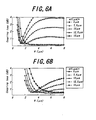
    Figure 6A is a diagram showing the relation between the waveguide size and the coupling loss with the optical fiber when the thickness of the core layer with the waveguide is 6µm, and Figure 6B is a diagram showing the relation between the waveguide size and the coupling loss with the optical fiber when the thickness of the core layer with the waveguide is 2µm.
    These are obtained by calculating the relation between the thickness T and the width W of the core layer and the coupling loss with the optical fiber by means of a steady state interface analysis using a finite element method.
    In this case, it is assumed that a material whose refractive index n is about 1.5 such as quartz, glass or polymer is used as the material of the waveguide, where the refractive index difference Δn between the core layer and the clad layer is 0.5% and the wavelength of the light propagating through the waveguide is 1.55µm. If the refractive index of the core layer is nc and the refractive index of the clad layer is ns, the refractive index difference Δn has the following relation: Δn = (nc - ns)/ns
    Symbol wf in Figures 6A and 6B represents the spot size of the light propagating through the optical fiber. In case of the conventional optical fiber, wf= 5µm.
    In case of the single-mode waveguide, provided that the thickness T is constant, the optical confinement is weakened and thus the spot size decrease as the width reduces. Therefore, if the coupling loss is small, the spot size wf is substantially realized by the waveguide size of itself.
    The light propagating through the waveguide with the width W and the thickness T different from each other generally has a shape similar to an ellipse. Assuming that the spot size in the lateral direction is wx and that in the vertical direction is wy, an effective spot size is represented by (wx x wy)1/2.
    As seen from Figure 6, if the refractive index difference Δn is 0.5% and the thickness T is constant, the spot size wf can be set at a proper size by changing the width W. For example, in order to set the spot size wf at 5µm, the width W is 7µm when the thickness T is 6µm, and the width W is 8-10µm when the thickness T is 2µm. In order to set the spot size wf at 10µm, the width W is 2µm when the thickness T is 6µm, and the width W is 4-4.5µm when the thickness T is 2µm. Therefore, the spot size wf can be set at a desired size by selecting the material of the waveguide, the refractive index difference Δn, the thickness T or the width W properly.
    Similar to the embodiment of the present invention shown in Figure 2, between waveguides different in spot size from each other, the tapered waveguides 28a, 28b, 29a and 29b gradually varying in width or thickness are formed and the taper length of theirself is set at a degree of several 10µm to several 100µm for example, and thereby the coupling loss between the waveguides can be reduced.
    Also, it is possible to determine the spot size as desired by having the cross waveguide with the same size as that of the waveguides in the other area and having the refractive index differences in the respective areasdifferent from one another. In this case, the refractive index differences among the tapered waveguides 28a, 28b, 29a and 29b vary gradually.
    As a method of increasing the spot size, a method of keeping the thickness of the core layer constant and making the width of the core layer narrow has been described, however, it is possible to apply a method of making the thickness of a core layer substantially thin and thus making the width of the core layer wide, or a method of constructing a waveguide structure comprising a plurality of waveguide layers, and it is possible to obtain effects of the present invention by adopting any spot size converting waveguide structure conventionally used. These waveguides can be formed by using a conventional photolithographic technique, a film forming technique, an epitaxial selective growth technique and so on.
    According to the present embodiment, it is possible to reduce the optical loss and the crosstalk in the optical device and improve the operating efficiency of the optical device by making the spot size of the light propagating through the cross waveguide larger than that of the light propagating through the optical input waveguide, the optical output waveguide or the connection waveguide.
    By having the substantially same spot size of the light input into the optical input waveguide as that of light output from the optical element or the optical waveguide to be connected to the optical input waveguide, it is possible to reduce the coupling loss between the optical input waveguide and such an optical element as a plane light circuit (PLC) or a semiconductor optical device or such an optical waveguide as an optical fiber.
    Further, it is possible to keep the whole loss of the optical device small because any other waveguide than the cross waveguide is formed so that the radiation loss is small by making the optical confinement strong and thus making the spot size of the light small.
    Figure 7 is a diagram showing a second embodiment of the optical device according to the present invention. This optical device comprises optical input waveguides 171a and 171b and optical output waveguides 172a and 172b each having the width W1 and the thickness T1, curved waveguides 173a, 173b, 174a and 174b each having the width W2 and the thickness T2, and a cross waveguide 175 having the width W3 and the thickness T3 as a core layer. In this case, it has relations of "W3 ≥ W1" and "T1 ≥ T3".
    Tapered waveguides 176, 177, 178 and 179 interposed between the curved waveguides 173a, 173b, 174a and 174b and the cross waveguide 175 have tapered portions 176a, 177a, 178a and 179a extending from the curved waveguides 173a, 173b, 174a and 174b, and tapered portions 176b, 177b, 178b and 179b extending from the cross waveguide 175.
    The spot size of the light is converted with a low loss by each of these tapered portions 176a, 177a, 178a and 179a and tapered portions 176b, 177b, 178b and 179b. In case of having relations of "W3 ≥ W1" and "T1 ≥ T3", it is also possible to compose these waveguides of the single core layer by forming the lateral width and the layer thickness of them into a tapered shape.
    In this embodiment, also, it is possible to reduce the optical loss and the crosstalk in the optical device and improve the operational efficiency of the device by making the spot size of the light propagating through the cross waveguide larger than that of the light propagating through the optical input waveguide, the optical output waveguide or the connection waveguide.
    Figure 8 is a diagram showing the relation between the width of a core layer with the thickness of 1µm or 2µm and the crosstalk of the second embodiment, and Figure 9 is a diagram showing the relation between the width of a core layer with the thickness of 2µm or 4µm and the crosstalk of the second embodiment. In Figure 8, the branch angle  is 4° and the refractive index difference between the core layer and the clad layer is 0.5%, and in Figure 9, the branch angle  is 4° and the refractive index difference between the core layer and the clad layer is 0.3%.
    As seen from Figures 8 and 9, the lager the width of the core layer is, the greater the crosstalk characteristic is, and a good crosstalk characteristic cannot be obtained if the width of a core layer is not more than 10µm like a conventional optical device. The larger the width of a core layer is, the greater the crosstalk characteristic is, however, if the width of the core layer is larger than a certain value, the waveguide comes into a multi-mode state and the loss increases.
    As seen from Figures 8 and 9, the thinner the width of a core layer is, the greater the crosstalk characteristic is if the width of the core layer is constant. In this embodiment, the branch/cross waveguide is of a single-mode waveguide structure.
    Further, in the second embodiment, it is possible to realize a crosstalk reduction effect being remarkably excellent in comparison with a conventional waveguide structure by making a structure having the optical confinement effect in the waveguide with the core layer much thinner than the ordinary waveguide structure. A principle for obtaining such an effect is described in the following.
    Figure 10 shows the distribution of the intensity of light waves propagating through a branch/cross waveguide in a section of the waveguide. The distribution of the intensity in the lateral direction (x direction) of a core layer c is nearly in the shape of a Gaussian distribution.
    On the other hand, the distribution of the intensity in the vertical direction (y direction) of the core layer c takes the shape of an exponential distribution different from the ordinary waveguide. This is caused by a fact that the spot size of the light waves in the vertical direction is substantially larger than the thickness T of the core layer c due to a small optical confinement effect in the waveguide in the vertical direction.
    In case of the waveguide with a normal optical confinement effect or the waveguide with a comparatively intense optical confinement effect like a conventional branch/cross waveguide, the distribution of the intensity of light waves takes a shape close to a Gaussian distribution in both the vertical direction and the lateral direction. As a result, in comparison with the crosstalk characteristic of the branch/cross waveguide through which light waves with a Gaussian distribution propagate(Figure 4), this embodiment has a characteristic different from that shown in Figure 4.
    Figures 11 to 13 show the relation between the crosstalk and the branch/cross angle  in case of setting the thickness of the core layer c at 4µm, 3µm and 2µm when the refractive index difference between the core layer and the clad layer is 0.2% in the present invention, respectively.
    Figure 11 shows a characteristic in case of forming a waveguide having a comparatively intense optical confinement effect by making the thickness T of a core layer c comparatively large. As shown in Figure 11, like the characteristic shown in Figure 4, as large the branch/cross angle  and the width W of the core layer c are, the greater the crosstalk characteristic. However, Figure 11 is different from Figure 4 in that the effect of improvement in the crosstalk is not remarkable even if the branch/cross angle  is comparatively large.
    In case of making the thickness T of the core layer c smaller, as shown in Figure 13, in a range of 3° to 6° in this embodiment, the larger the branch/cross angle  is, the greater the crosstalk is. However, when the branch/cross angle  is larger than 6°, the crosstalk characteristic tends to be worse.
    In this case, as the optical confinement effect in the vertical direction is comparatively small, the light waves propagating through the core layer c have the distribution of the intensity in the shape of the exponential distribution as shown in Figure 10. Such light waves in the shape of the exponential distribution have a substantially small spot size in the central part (core part) of the optical waveguide, namely, they have properties obtained by superposing the light waves being effectively intense in the optical confinement on light waves being comparatively larger in the spot size in the periphery (clad part) of the optical waveguide.
    Because of this, a component with an effectively large spot size in the branch/cross waveguide propagates as spreading in a comparatively wide angle in the direction of the propagation of the light waves due to an effect of diffraction. In case of setting the cross/branch angle  at the substantially same degree as such a spreading angle, the diffracted light tends to couple to the branch/cross waveguide and comes to make the crosstalk worse.
    In this embodiment, therefore, there is the optimum cross/branch angle  with a good crosstalk in a range of comparatively small angles. The optimum cross/branch angle  depends on the material, the refractive index difference and the structure of the optical waveguide. When the cross/branch angle  is larger than 8°, the crosstalk characteristic tends to be improved as the cross/branch angle  increases similar to the construction of the optical waveguide throught which the light waves in the shape of a normal Gaussian distribution propagate.
    Figures 8 and 9 have respectively shown the cases that the refractive index difference between the core layer and the clad layer is 0.5% and 0.3%, respectively, however, in case that the refractive index of the core layer is different from that of the clad layer, an effect of the present invention can be obtained by properly setting the width and the thickness of the core layer according to the refractive index difference between these layers.
    Figure 14A is a top view of a third embodiment of the optical device according to the present invention, and Figure 14B shows a section III-III of Figure 14A. This embodiment takes a 2 x 2 switch form by arranging an electrode 42 just above the cross part of a cross waveguide 41. The present invention can be also applied to such an optical switch of the 2 x 2 switch form.
    Figure 15 is a diagram showing a fourth embodiment of the optical device according to the present invention. This has a 2 x 2 switch form with a cross waveguide 51 and four electrodes 44a, 44b, 44c and 44d, and the present invention can be also applied to this.
    Figure 16 is a diagram showing a fifth embodiment of the optical device according to the present invention. This forms a matrix switch, and comprises core layers 51 with optical waveguides, a clad layer 52, optical fibers 53 connected to the input side and output side, cross waveguides 54 and optical switch elements 55.
    A cross waveguide structure of the above-mentioned optical switch portion may be used as the cross waveguide 54, and any of the first type of the switch and the second type of the switch may be used as the optical switch element 55. In this case it is possible to realize an optical switch matrix to which the present invention is applied.
    Although the case where the single-mode optical waveguide is used as the optical waveguide has been described hereinbefore, when using the waveguide with a small length or that formed with a high accuracy waveguide processing technique, it is possible to apply the present invention because a low mode conversion loss can be achieved even if the multi-mode optical waveguide is used as a part of the optical device. Furthermore, the present invention can be applied to the case of using the multi-mode optical waveguide as the whole optical waveguides.
    The above-mentioned embodiments can be applied to all optical devices such as a semiconductor optical waveguide device utilizing a plasma effect caused by carriers in a semiconductor, a multiple quantum well structure effect and the like, and a ferroelectric optical waveguide device composed of lithium niobate or the like utilizing an EO effect, and they are each formed of an optical device composed of glass, polymer and the like utilizing a TO effect as the most suitable ones.
    Figure 17 is a diagram showing a sixth embodiment of the optical device according to the present invention. This shows a section of the central part of a cross waveguide, and comprises a core layer 101 of the refractive index n having an optical waveguide, a first clad layer 102 of refractive index ns1 and the thickness ts1, a second clad layer 103 of the refractive index ns2 and the thickness ts2, an electrode 104 for changing the refractive index of the cross waveguide by applying a certain voltage or supplying a certain current, and a substrate 105.
    In this embodiment, the core layer 101, the clad layer 102 and the clad layer 103 are each formed of a polymer material such as polyimide with a negative temperature coefficient, and the relation among the refractive indexes is: nc>ns2>ns1.
    Figure 18 is a diagram showing an effective temperature distribution at a vicinity of a cross waveguide of the conventional optical device in which the first clad layer has the same refractive index as that of the second clad layer, and Figures 19 to 21 are diagrams each showing an effective temperature distribution at a vicinity of a cross waveguide of an optical device according to the present invention in which the refractive index of the first clad layer is different from that of the second clad layer. These temperature distributions represent values calculated by the finite element method, and the numerical ranges in the figures represent respectively values normalized by the temperature of the electrodes 113, 123, 133 and 143 taking the temperature of a substrate not shown in figures as a reference value. The thicknesses of the first clad layers 111, 121, 131 and 141 are respectively 30µm, and the thicknesses of the second clad layers 112, 122, 132 and 142 are respectively 10µm. The first clad layers 111, 121, 131 and 141, the second clad layers 112, 122, 132 and 142, and the core layers 114, 124, 134 and 144 are each composed of the polyimide material.
    The polyimide material has a TO effect in which the refractive index decreases as the temperature increases. Therefore, these temperature distributions correspond to the spatial distributions of the refractive index change portions based on the TO effect, and shows that the refractive index decreases as the temperature increases.
    As seen from Figure 18, an isothermal line of the distribution of temperature comes into a state closer to the perpendicularity to the x-axis and the temperature increases as being closer to the electrode 113. However, if the cross waveguide, namely, the core part 114 is close to the electrode 113, the absorption loss of the light is caused by the electrode 113. Reducing such an influence and considering the perpendicularity of a high-temperature and isothermal line to the x-axis and a required switching speed, the position of the core layer 114 as well as the sum of the thickness of the first clad layer 111 and that of the second clad layer 112 are determined.
    In this case, it is preferable to set the center of the core layer 114 at a position being about 10µm in depth from the surface of the second clad layer 112 and about 10 to 20µm apart in the x-axis direction from an end of the electrode 113. However, there is a disadvantage that a part of the reflection light is radiated due to a fact that an isothermal line of the temperature distribution is inclined to a y-z axis plane, namely, a plane perpendicular to the x-axis at a vicinity of the core layer 114, and the total reflection surface of light input into the cross waveguide is deviated from the plane perpendicular to the x-axis.
    In Figures 19 to 21, the first clad layers 121, 131 and 141 have a lower refractive index than that of the second clad layers 122, 132 and 142. In Figure 19, the difference in the refractive index between the first clad layers 121, 131 and 141 and the second clad layers 122, 132 and 142 is 0.05%, in Figure 20, the refractive index difference is 0.1%, and in Figure 21, the refractive index difference is 0.2%.
    In Figures 19 to 21, also, an actual temperature distribution in the first clad layers 121, 131 and 141 and the second clad layers 122, 132 and 142 is similar to Figure 15, however, when considering that the polyimide has the TO effect with the negative temperature coefficient of about -1 x 10⁻⁴/°C, the whole first clad layers 121, 131 and 141 result in being raised in temperature by 1°C per the refractive index difference of 0.01% between the first clad layers 121, 131 and 141 and the second clad layers 122, 132 and 142.
    For example, when the electrodes 123, 133 and 143 are raised by 100°C in temperature, the first clad layers 121, 131 and 141 are larger by 0.01 in terms of normalized temperature per refractive index difference of 0.01%. It is Figures 16 to 18 that shows the result of calculation of an effective temperature distribution obtained by considering such an effect. That is to say, when the refractive index difference is set at about 0.05% to 0.1%, the temperature distribution (isothermal line) at a vicinity of the core layer is substantially perpendicular to the x-axis.
    With the utilization of this principle, the loss and the crosstalk caused by the total reflection of the light can be reduced by considering the influence of the TO effect or the EO effect of the waveguide material and the position of a core layer, and properly setting the thickness and the refractive index difference of the clad layer. In case of using, for example, a polymer material as a waveguide material, magnitude of the refractive index can be set by a proper combination of ingredients and the like, the thickness can be set by adjusting the viscosity of an unhardened polymer material or the rotation speed of a spinner, and these waveguide structures can be realized by using a conventional photolithographic technique or film forming technique.
    Figure 22 is a diagram showing a seventh embodiment of the optical device according to the present invention. This shows a section of the central part of a cross waveguide, and comprises a core layer 151 of the refractive index nc having the optical waveguide, a first clad layer 152 of the refractive index ns11 and the thickness ts11, a second clad layer 153 of the refractive index ns1 and the thickness ts12, a third clad layer 154 of the refractive index ns13 and the thickness ts13, an electrode 155 for changing the refractive index of the cross waveguide by applying a certain voltage or supplying a certain current, and a substrate 156.
    In this embodiment, the core layer 151, the clad layer 152, the clad layer 153 and the clad layer 154 are each composed of the polymer material such as the polyimide with the negative temperature coefficient, and the relation among the refractive indexes is: nc > ns12 > ns11 > ns13.
    The present invention can be also applied to a case of further comprising the third clad layer 154 in this way. Two or more clad layers may be interposed between the second clad layer and the substrate.
    Figure 23A is a top view of an eighth embodiment of the optical device according to the present invention, and Figure 23B shows a section IV-IV of Figure 23A. In this embodiment, two electrodes 162 and 163 are arranged above a branch waveguide 161. The present invention can be also applied to this case.
    Although a case of using the polyimide material with the negative temperature coefficient has been described hereinbefore in order to obtain the TO effect, it is possible also to form the core layer and the clad layer using a material with a positive temperature coefficient. In case of using LiNbO3, PLZT, optical glass and the like as such a material, in the fifth embodiment, the refractive indexes need to have the following relation: ns2 < ns1, and in the seventh embodiment, the refractive indexes need to have the following relation: ns12<ns11 <ns13.
    In case of utilizing the EO effect, it is enough to utilizing a current injection effect (plasma effect) of a semiconductor to the distribution of the intensity of the electric field formed by an applied voltage between the electrode and the substrate and set the refractive index and the thickness of the clad layer, and the principle of the present invention can be also applied to any optical material.
    Next, the relation between the thickness and the coupling loss of the first clad layer (for example, a clad layer 102 in Figure 7) is described with reference to Figures 24 and 25.
    As shown in Figure 24, if the thickness of the first clad layer is smaller than 15µm, the coupling loss decreases. When the thickness of the first clad layer is smaller than 4µm, however, the light may leak from the first clad layer, and thus the propagation loss may degrade. As a result, it is preferable to have the thickness of the first clad layer not less than 4µm.
    On the other hand, when the thickness of the first clad layer is not less than 15µm, the coupling loss is substantially saturated and a substantial reduction of the coupling loss is not achieved. And as shown in Figure 25, when the thickness of the first clad layer exceeds 40µm, the rate of the increase of the power supply is remarkable. As a result, the thickness of the first clad layer is preferably not more than 40µm, and more preferably, it is not more than 15µm.
    Next, in case of the 2 x 2 optical device (a 2-input and 2-output type of an optical switch), the ratio of the width of the electrode to that of the optical waveguide in a preferable embodiment of the present invention is described with reference to Figures 26 to 28 in comparison with a conventional optical device.
    As a conventional 2 x 2 optical device uses a waveguide whose core layer has a comparatively large sectional area and which has a remarkably intense optical confinement effect, it is necessary to have a comparatively narrow width t of an electrode 272 arranged in the central part near the branch waveguide, namely, the ratio (t/d) of the width t of the electrode 272 to the width d of the waveguide in Figure 26 in order to have the excessive loss as small as possible. In case that the width t is small, however, it is difficult to align the electrode 272 with the branch waveguide 271, and making an electric current flow through the electrode 272 is liable to cause the breaking of wire.
    According to the preferred embodiment of the present invention, by using the single-mode optical waveguide having a comparatively small sectional area of the core layer and with the optical confinement not being substantially intense, the width t of the electrode 274 arranged near the branch waveguide 273 shown in Figure 27, namely, the ratio (t/d) of the width t to the width d of the waveguide is comparatively large, and thus an optical switching is performed in such a manner that the light passes through the first clad layer 275 from the branch optical waveguide 273 and propagates again through the branch waveguide 273 as shown by an arrow.
    Figure 28 shows the relation between the loss in the switching operation (the reflection loss) and a standard value t/d of the electrode width in the 2 x 2 optical devices of the prior art and the present invention. Here, the shape of a core (T/d, T: core thickness) is taken as a parameter. It is found from Figure 28 that in the optical device using a conventional optical waveguide with an intense optical confinement, if t/d is very small, the loss is small, however, the loss increases remarkably as the t/d increases. In this phenomenon, the electrode end parts 272-1 and 272-2 function as the total reflection surfaces to the wave-guided light in the switching operation, and as t/d increases, the reflected light leaks to the clad and causes a substantial loss.
    On the other hand, according to the present invention, when t/d is small, a slight excess loss occurs in the switching operation. This is caused by the loss occurring at the branch/cross part because of using the single-mode waveguide with a weak confinement. However, it is possible to suppress the loss to a slight increase though t/d increases. The reason is that in the present invention as the third clad layer 154 having a relatively small refractive index as shown in Figure 22 is arranged, the reflected light leaking to the clad region 275 is coupled again into the branch waveguide 273 and the increase of loss is suppressed. Therefore, if t/d is not less than 0.2, the reflection loss can be greatly reduced in comparison with the prior art.
    If the width t of the electrode 274 is larger than a value in a certain range, there is a problem that the power consumption of the electrode increases. Also, when the width of a region functioning as the core layer increases and the light reaches the output side of the waveguide, evanescent waves at the region functioning as the core layer leak to the output side of the waveguide and the extinction ratio decreases. Therefore, the optimum range of the width t of the electrode 274 depends on the thickness of the clad layer and the width d of the core layer, and the maximum extinction ratio is obtained by making the width t not more than 3 times the width d of the core layer 271.
    While the present invention has been described above with reference to certain preferred embodiments, it should be noted that they were present by way of examples only and various changes and/or modifications may be made without departing from the scope of the invention. For example, the present invention can be also applied to an optical device having a single input waveguide, not less than three output waveguides and a branch waveguide for connecting them, an optical device having not less than three input waveguides, a single output waveguide and a branch waveguide for connecting them, an optical device having not less than two input waveguides, not less than three output waveguides and a cross waveguide for connecting them, or an optical device having not less than three input waveguides, not less than two output waveguides and a cross waveguide for connecting them.
    In the above-mentioned embodiments, an optical device provided with an optical switch has been described, however, the present invention can be also applied to an optical device without an optical switch.
    In the first embodiment, the case where the spot size of the light propagating through the branch/cross waveguide is larger than that of the light propagating through the optical input waveguide, the optical output waveguide or the connection waveguide has been described, however, when the spot size of the light propagating through the branch/cross waveguide is not less than 5µm, it is possible to have a small loss of the optical input waveguide, the optical output waveguide or the connection waveguide and have a small diffraction of the light at the branch/cross waveguide regardless of the spot size of the light propagating through the optical input waveguide, the optical output waveguide or the connection waveguide, and thus it is possible to reduce the optical loss and crosstalk in the optical device. Such an optical device can be formed by coupling light input into the optical input waveguide with a lens or a spot magnifying waveguide and coupling light output from the optical output waveguide with the lens or the spot magnifying waveguide in the optical switch in Figure 1, for example. In this case, for example, the spot size of each light propagating through the branch/cross waveguide, the optical input waveguide, the optical output waveguide and the connection waveguide is not less than 5µm.

    Claims (22)

    1. An optical device comprising;
      an optical input waveguide,
      a branch/cross waveguide,
      an optical output waveguide, and
      connection waveguides for respectively connecting said optical input waveguide and said branch/cross waveguide and connecting said optical output waveguide and said branch/cross waveguide to each other,
         wherein the spot size of light propagating through said branch/cross waveguide is larger than the spot size of light propagating through said optical input waveguide, said optical output waveguide, or said connection waveguide.
    2. The device according to claim 1, wherein the spot size of light propagating through said branch/cross waveguide is not less than 5µm, and the spot size of light propagating through said optical input waveguide, said optical output waveguide or said connection waveguide is less than 5µm.
    3. An optical device comprising;
      an optical input waveguide,
      a branch/cross waveguide,
      an optical output waveguide, and
      connection waveguides for respectively connecting said optical input waveguide and said branch/cross waveguide and connecting said optical output waveguide and said branch/cross waveguide to each other,
         wherein; the spot size of light propagating through said branch/cross waveguide is not less than 5µm.
    4. The device according to any one of claims 1 to 3, wherein at least one of the width and the thickness of said branch/cross waveguide is set at a value smaller than the width or the thickness of said optical input waveguide and said optical output waveguide.
    5. The device according to any one of claims 1 to 4, wherein the ratio of the width to the thickness of said branch/cross waveguide is not less than 10/4.
    6. An optical device comprising;
      an optical input waveguide,
      a branch/cross waveguide,
      an optical output waveguide, and
      connection waveguides for respectively connecting said optical input waveguide and said branch/cross waveguide and connecting said optical output waveguide and said branch/cross waveguide to each other,
         wherein at least one of the width and the thickness of said branch/cross waveguide is set at a value smaller than the width or the thickness of said optical input waveguide and said optical output waveguide.
    7. An optical device comprising;
      an optical input waveguide,
      a branch/cross waveguide,
      an optical output waveguide, and
      connection waveguides for respectively connecting said optical input waveguide and said branch/cross waveguide and connecting said optical output waveguide and said branch/cross waveguide to each other,
         wherein the ratio of the width to the thickness of said branch/cross waveguide is not less than 10/4.
    8. The device according to any one of claims 1 to 7, wherein the width and the thickness of said branch/cross waveguide are not less than 10µm and not more than 4µm, respectively.
    9. The device according to any one of claims 1 to 8, wherein the cross/branch angle of said branch/cross waveguide is 3 to 6 degrees.
    10. The device according to any one of claims 1 to 9, wherein said branch/cross waveguide consists of a single-mode waveguide.
    11. The device according to any one of claims 1 to 10, wherein said connection waveguide has a tapered waveguide.
    12. The device according to any one of claims 1 to 11, wherein the spot size of light input into said optical input waveguide is substantially equal to the spot size of light output from an optical element or an optical waveguide to be connected to said optical input waveguide.
    13. The device according to any one of claims 1 to 12, wherein the spot size of light output from said optical output waveguide is substantially equal to the spot size of light input into an optical element or an optical waveguide to be connected to said optical output waveguide.
    14. The device according to any one of claims 1 to 13, further comprising an optical switch for switching over the direction of propagation of light input into said branch/cross waveguide.
    15. The device according to claim 14, wherein said optical switch has at least one electrode for changing the refractive index of said branch/cross waveguide by applying a certain voltage or supplying a certain current.
    16. An optical device comprising;
      a core layer having a branch/cross waveguide,
      a first clad layer having a specific refractive index, with said core layer being deposited on a part of surface of said first clad layer,
      a second clad layer having a refractive index different from the refractive index of said first clad layer, with said core layer being provided between said first clad layer and said second clad layer, and
      at least one electrode for changing the refractive index of said branch/cross waveguide by applying a certain voltage or supplying a certain current.
    17. The device according to claim 16, wherein the thickness of said first clad layer is between 4µm and 40µm.
    18. An optical device according to claim 17, wherein the thickness of said first clad layer is between 4µm and 15µm.
    19. The device according to any one of claims 16 to 18, wherein said core layer has a single-mode optical input waveguide, a single-mode branch/cross waveguide and a single-mode optical output waveguide,
      said electrode is a rectangular electrode disposed near said single-mode branch/cross waveguide,
      the ratio of the width of said electrode to that of said waveguide is not less than 0.2, so that said optical device has a function of switching the light so as to pass through said first clad layer from said single-mode branch/cross waveguide and propagate again through said single-mode branch/cross waveguide.
    20. The device according to any one of claims 16 to 18, wherein said core layer has a single-mode optical input waveguide, a single-mode branch/cross waveguide and a single-mode optical output waveguide,
      said electrode is a rectangular electrode disposed near said single-mode branch/cross waveguide,
      the ratio of the width of said electrode to that of said waveguide is not more than 3, and
      said optical device has a function of switching the light so as to pass through said first clad layer from said single-mode branch/cross waveguide and propagate again through said single-mode branch/cross waveguide.
    21. The device according to any one of claims 16 to 20, wherein each of said first clad layer and said second clad layer consists of a material having a negative temperature coefficient, and the refractive index of said first clad layer is lower than that of said second clad layer.
    22. The device according to any one of claims 16 to 20, wherein each of said first clad layer and said second clad layer consists of a material having a positive temperature coefficient, and the refractive index of said first clad layer is higher than that of said second clad layer.
    EP01965559A 2000-09-18 2001-09-06 Optical device Expired - Lifetime EP1319973B1 (en)

    Applications Claiming Priority (9)

    Application Number Priority Date Filing Date Title
    JP2000281363 2000-09-18
    JP2000281363 2000-09-18
    JP2000316071 2000-10-17
    JP2000316071 2000-10-17
    JP2001095848 2001-03-29
    JP2001095848 2001-03-29
    JP2001192855 2001-06-26
    JP2001192855 2001-06-26
    PCT/JP2001/007744 WO2002023264A1 (en) 2000-09-18 2001-09-06 Optical device

    Publications (3)

    Publication Number Publication Date
    EP1319973A1 true EP1319973A1 (en) 2003-06-18
    EP1319973A4 EP1319973A4 (en) 2004-07-14
    EP1319973B1 EP1319973B1 (en) 2007-03-07

    Family

    ID=27481615

    Family Applications (1)

    Application Number Title Priority Date Filing Date
    EP01965559A Expired - Lifetime EP1319973B1 (en) 2000-09-18 2001-09-06 Optical device

    Country Status (5)

    Country Link
    US (1) US7184631B2 (en)
    EP (1) EP1319973B1 (en)
    JP (1) JPWO2002023264A1 (en)
    DE (1) DE60127146T2 (en)
    WO (1) WO2002023264A1 (en)

    Cited By (1)

    * Cited by examiner, † Cited by third party
    Publication number Priority date Publication date Assignee Title
    EP1406114A4 (en) * 2001-04-18 2006-01-18 Ngk Insulators Ltd Optical device

    Families Citing this family (10)

    * Cited by examiner, † Cited by third party
    Publication number Priority date Publication date Assignee Title
    DE10253438B4 (en) * 2002-11-12 2008-09-18 Finisar Corp., Sunnyvale Cross waveguide
    US6934446B2 (en) * 2003-03-27 2005-08-23 Lucent Technologies Inc. Optical waveguiding apparatus having reduced crossover losses
    JP4585990B2 (en) * 2006-06-30 2010-11-24 日本電信電話株式会社 Waveguide type optical circuit
    JP5176150B2 (en) * 2009-01-13 2013-04-03 富士通株式会社 Optical device and optical transmitter
    US8401345B2 (en) * 2010-06-16 2013-03-19 Oracle America, Inc. Optical modulator with three-dimensional waveguide tapers
    US20120243826A1 (en) * 2011-03-21 2012-09-27 Liping Sun Low power compact optical switch
    KR101900630B1 (en) * 2014-07-16 2018-09-19 후아웨이 테크놀러지 컴퍼니 리미티드 Cross waveguide
    CN107346047B (en) * 2016-05-04 2020-04-21 华为技术有限公司 an optical switch
    US10816725B2 (en) * 2018-09-18 2020-10-27 Globalfoundries Inc. Waveguide intersections incorporating a waveguide crossing
    WO2025253586A1 (en) * 2024-06-06 2025-12-11 Ntt株式会社 Mode converter and optical connector

    Family Cites Families (14)

    * Cited by examiner, † Cited by third party
    Publication number Priority date Publication date Assignee Title
    CA1123642A (en) * 1979-07-04 1982-05-18 Alexander W. Lightstone Multimode optical fiber coupler
    JPS6086530A (en) * 1983-10-18 1985-05-16 Nec Corp Waveguide type optical switch
    US4763977A (en) * 1985-01-09 1988-08-16 Canadian Patents And Development Limited-Societe Optical fiber coupler with tunable coupling ratio and method of making
    CA1253376A (en) * 1985-07-29 1989-05-02 Kenneth O. Hill Fiber optic directional coupler
    GB8522704D0 (en) 1985-09-13 1985-10-16 British Telecomm Optical waveguide devices
    JPS6325631A (en) * 1986-07-18 1988-02-03 Oki Electric Ind Co Ltd Waveguide type optical switch
    JPH023025A (en) * 1988-06-17 1990-01-08 Fujitsu Ltd Semiconductor optical switch
    US5321782A (en) * 1991-01-07 1994-06-14 Furukawa Electric Co., Ltd. Directional coupler type optical function element
    US5623568A (en) * 1995-09-15 1997-04-22 Lucent Technologies Inc. Compact and fabrication tolerant high speed digital optical Y-switches
    DE19549245C2 (en) * 1995-12-19 2000-02-17 Hertz Inst Heinrich Thermo-optical switch
    JPH09189817A (en) * 1996-01-09 1997-07-22 Mitsubishi Gas Chem Co Inc Optical waveguide for optical splitter
    JPH1115028A (en) * 1997-06-19 1999-01-22 Nippon Telegr & Teleph Corp <Ntt> Polymer thermo-optical switch
    JP2000180646A (en) 1998-12-16 2000-06-30 Fujitsu Ltd Optical circuit device
    US6600843B2 (en) * 2001-03-13 2003-07-29 Srico, Inc. Optical modulator

    Cited By (1)

    * Cited by examiner, † Cited by third party
    Publication number Priority date Publication date Assignee Title
    EP1406114A4 (en) * 2001-04-18 2006-01-18 Ngk Insulators Ltd Optical device

    Also Published As

    Publication number Publication date
    DE60127146T2 (en) 2007-11-22
    JPWO2002023264A1 (en) 2004-01-22
    WO2002023264A1 (en) 2002-03-21
    EP1319973A4 (en) 2004-07-14
    US20020159706A1 (en) 2002-10-31
    EP1319973B1 (en) 2007-03-07
    US7184631B2 (en) 2007-02-27
    DE60127146D1 (en) 2007-04-19

    Similar Documents

    Publication Publication Date Title
    US20020006245A1 (en) Optical circuit
    EP0484878B1 (en) Y-branching optical circuit
    EP1319973B1 (en) Optical device
    US4818063A (en) Optical modulating/switching device
    KR19990052202A (en) Electro-optic polymer optical waveguide device structure to reduce driving voltage and loss
    JPH07318986A (en) Waveguide type optical switch
    US6529647B2 (en) Optical device with optical waveguides and manufacturing method therefor
    EP1278098B1 (en) Planar lightwave circuit type variable optical attenuator
    US7373025B2 (en) Waveguide-type optical device
    US20050196092A1 (en) Optical modulator and communications system
    JP2001350046A (en) Integrated optical waveguide element
    US6961493B2 (en) Optical device
    KR100400890B1 (en) Variable optical attenuator of in-line type and fabrication method thereof
    JP3077719B2 (en) Thermo-optic phase shifter
    EP0585468B1 (en) Waveguide type optical part
    RU2781367C1 (en) Hybrid integrated optical device
    JP2613942B2 (en) Waveguide type optical device
    US5815609A (en) Waveguide type optical external modulator
    JP6260631B2 (en) Optical waveguide device
    JPH06250131A (en) Light control element
    KR100370278B1 (en) Optical Path Controlling two by two Optical Switch
    JPH05297420A (en) Optical switch
    JP2643927B2 (en) Manufacturing method of optical branching / optical coupling circuit
    JP3481710B2 (en) Method for manufacturing optical waveguide body
    JPH0697287B2 (en) Light control circuit manufacturing method

    Legal Events

    Date Code Title Description
    PUAI Public reference made under article 153(3) epc to a published international application that has entered the european phase

    Free format text: ORIGINAL CODE: 0009012

    17P Request for examination filed

    Effective date: 20020614

    AK Designated contracting states

    Designated state(s): AT BE CH CY DE DK ES FI FR GB GR IE IT LI LU MC NL PT SE TR

    RIC1 Information provided on ipc code assigned before grant

    Ipc: 7G 02B 6/12 B

    Ipc: 7G 02F 1/313 A

    RBV Designated contracting states (corrected)

    Designated state(s): DE FR GB IT

    A4 Supplementary search report drawn up and despatched

    Effective date: 20040528

    17Q First examination report despatched

    Effective date: 20040812

    GRAP Despatch of communication of intention to grant a patent

    Free format text: ORIGINAL CODE: EPIDOSNIGR1

    GRAS Grant fee paid

    Free format text: ORIGINAL CODE: EPIDOSNIGR3

    GRAA (expected) grant

    Free format text: ORIGINAL CODE: 0009210

    AK Designated contracting states

    Kind code of ref document: B1

    Designated state(s): DE FR GB IT

    REG Reference to a national code

    Ref country code: GB

    Ref legal event code: FG4D

    REF Corresponds to:

    Ref document number: 60127146

    Country of ref document: DE

    Date of ref document: 20070419

    Kind code of ref document: P

    ET Fr: translation filed
    PLBE No opposition filed within time limit

    Free format text: ORIGINAL CODE: 0009261

    STAA Information on the status of an ep patent application or granted ep patent

    Free format text: STATUS: NO OPPOSITION FILED WITHIN TIME LIMIT

    26N No opposition filed

    Effective date: 20071210

    PGFP Annual fee paid to national office [announced via postgrant information from national office to epo]

    Ref country code: FR

    Payment date: 20100920

    Year of fee payment: 10

    Ref country code: IT

    Payment date: 20100917

    Year of fee payment: 10

    PGFP Annual fee paid to national office [announced via postgrant information from national office to epo]

    Ref country code: GB

    Payment date: 20100809

    Year of fee payment: 10

    PGFP Annual fee paid to national office [announced via postgrant information from national office to epo]

    Ref country code: DE

    Payment date: 20100930

    Year of fee payment: 10

    GBPC Gb: european patent ceased through non-payment of renewal fee

    Effective date: 20110906

    PG25 Lapsed in a contracting state [announced via postgrant information from national office to epo]

    Ref country code: IT

    Free format text: LAPSE BECAUSE OF NON-PAYMENT OF DUE FEES

    Effective date: 20110906

    REG Reference to a national code

    Ref country code: FR

    Ref legal event code: ST

    Effective date: 20120531

    REG Reference to a national code

    Ref country code: DE

    Ref legal event code: R119

    Ref document number: 60127146

    Country of ref document: DE

    Effective date: 20120403

    PG25 Lapsed in a contracting state [announced via postgrant information from national office to epo]

    Ref country code: DE

    Free format text: LAPSE BECAUSE OF NON-PAYMENT OF DUE FEES

    Effective date: 20120403

    PG25 Lapsed in a contracting state [announced via postgrant information from national office to epo]

    Ref country code: GB

    Free format text: LAPSE BECAUSE OF NON-PAYMENT OF DUE FEES

    Effective date: 20110906

    Ref country code: FR

    Free format text: LAPSE BECAUSE OF NON-PAYMENT OF DUE FEES

    Effective date: 20110930