EP1318592A2 - Bi-directional dc/dc converter and control method therefor - Google Patents
Bi-directional dc/dc converter and control method therefor Download PDFInfo
- Publication number
- EP1318592A2 EP1318592A2 EP02079897A EP02079897A EP1318592A2 EP 1318592 A2 EP1318592 A2 EP 1318592A2 EP 02079897 A EP02079897 A EP 02079897A EP 02079897 A EP02079897 A EP 02079897A EP 1318592 A2 EP1318592 A2 EP 1318592A2
- Authority
- EP
- European Patent Office
- Prior art keywords
- power
- switching
- power converter
- controller
- coupled
- Prior art date
- Legal status (The legal status is an assumption and is not a legal conclusion. Google has not performed a legal analysis and makes no representation as to the accuracy of the status listed.)
- Withdrawn
Links
- 238000000034 method Methods 0.000 title claims abstract description 42
- 238000005259 measurement Methods 0.000 claims abstract description 16
- 230000004044 response Effects 0.000 claims abstract description 6
- 238000006243 chemical reaction Methods 0.000 claims description 25
- 238000012935 Averaging Methods 0.000 claims description 5
- 238000012544 monitoring process Methods 0.000 claims description 4
- 230000008878 coupling Effects 0.000 claims 3
- 238000010168 coupling process Methods 0.000 claims 3
- 238000005859 coupling reaction Methods 0.000 claims 3
- 238000002955 isolation Methods 0.000 description 13
- 230000001360 synchronised effect Effects 0.000 description 12
- 238000004590 computer program Methods 0.000 description 5
- 230000008569 process Effects 0.000 description 5
- 230000033228 biological regulation Effects 0.000 description 3
- 239000003990 capacitor Substances 0.000 description 3
- 230000008859 change Effects 0.000 description 3
- 238000013461 design Methods 0.000 description 3
- 230000009977 dual effect Effects 0.000 description 3
- 230000006872 improvement Effects 0.000 description 3
- 230000008901 benefit Effects 0.000 description 2
- 230000003247 decreasing effect Effects 0.000 description 2
- 230000005669 field effect Effects 0.000 description 2
- 230000003321 amplification Effects 0.000 description 1
- 238000013459 approach Methods 0.000 description 1
- 230000005540 biological transmission Effects 0.000 description 1
- 238000012937 correction Methods 0.000 description 1
- 230000007423 decrease Effects 0.000 description 1
- 238000007599 discharging Methods 0.000 description 1
- 238000009429 electrical wiring Methods 0.000 description 1
- 230000005670 electromagnetic radiation Effects 0.000 description 1
- 238000005516 engineering process Methods 0.000 description 1
- 239000000835 fiber Substances 0.000 description 1
- 239000000446 fuel Substances 0.000 description 1
- 229910044991 metal oxide Inorganic materials 0.000 description 1
- 150000004706 metal oxides Chemical class 0.000 description 1
- 238000003199 nucleic acid amplification method Methods 0.000 description 1
- 238000012545 processing Methods 0.000 description 1
- 230000009467 reduction Effects 0.000 description 1
- 239000004065 semiconductor Substances 0.000 description 1
- 239000000126 substance Substances 0.000 description 1
- 238000006467 substitution reaction Methods 0.000 description 1
Images



Classifications
-
- H—ELECTRICITY
- H02—GENERATION; CONVERSION OR DISTRIBUTION OF ELECTRIC POWER
- H02M—APPARATUS FOR CONVERSION BETWEEN AC AND AC, BETWEEN AC AND DC, OR BETWEEN DC AND DC, AND FOR USE WITH MAINS OR SIMILAR POWER SUPPLY SYSTEMS; CONVERSION OF DC OR AC INPUT POWER INTO SURGE OUTPUT POWER; CONTROL OR REGULATION THEREOF
- H02M3/00—Conversion of DC power input into DC power output
- H02M3/02—Conversion of DC power input into DC power output without intermediate conversion into AC
- H02M3/04—Conversion of DC power input into DC power output without intermediate conversion into AC by static converters
- H02M3/10—Conversion of DC power input into DC power output without intermediate conversion into AC by static converters using discharge tubes with control electrode or semiconductor devices with control electrode
- H02M3/145—Conversion of DC power input into DC power output without intermediate conversion into AC by static converters using discharge tubes with control electrode or semiconductor devices with control electrode using devices of a triode or transistor type requiring continuous application of a control signal
- H02M3/155—Conversion of DC power input into DC power output without intermediate conversion into AC by static converters using discharge tubes with control electrode or semiconductor devices with control electrode using devices of a triode or transistor type requiring continuous application of a control signal using semiconductor devices only
- H02M3/156—Conversion of DC power input into DC power output without intermediate conversion into AC by static converters using discharge tubes with control electrode or semiconductor devices with control electrode using devices of a triode or transistor type requiring continuous application of a control signal using semiconductor devices only with automatic control of output voltage or current, e.g. switching regulators
- H02M3/158—Conversion of DC power input into DC power output without intermediate conversion into AC by static converters using discharge tubes with control electrode or semiconductor devices with control electrode using devices of a triode or transistor type requiring continuous application of a control signal using semiconductor devices only with automatic control of output voltage or current, e.g. switching regulators including plural semiconductor devices as final control devices for a single load
- H02M3/1582—Buck-boost converters
-
- H—ELECTRICITY
- H02—GENERATION; CONVERSION OR DISTRIBUTION OF ELECTRIC POWER
- H02M—APPARATUS FOR CONVERSION BETWEEN AC AND AC, BETWEEN AC AND DC, OR BETWEEN DC AND DC, AND FOR USE WITH MAINS OR SIMILAR POWER SUPPLY SYSTEMS; CONVERSION OF DC OR AC INPUT POWER INTO SURGE OUTPUT POWER; CONTROL OR REGULATION THEREOF
- H02M3/00—Conversion of DC power input into DC power output
- H02M3/02—Conversion of DC power input into DC power output without intermediate conversion into AC
- H02M3/04—Conversion of DC power input into DC power output without intermediate conversion into AC by static converters
- H02M3/10—Conversion of DC power input into DC power output without intermediate conversion into AC by static converters using discharge tubes with control electrode or semiconductor devices with control electrode
- H02M3/145—Conversion of DC power input into DC power output without intermediate conversion into AC by static converters using discharge tubes with control electrode or semiconductor devices with control electrode using devices of a triode or transistor type requiring continuous application of a control signal
- H02M3/155—Conversion of DC power input into DC power output without intermediate conversion into AC by static converters using discharge tubes with control electrode or semiconductor devices with control electrode using devices of a triode or transistor type requiring continuous application of a control signal using semiconductor devices only
- H02M3/156—Conversion of DC power input into DC power output without intermediate conversion into AC by static converters using discharge tubes with control electrode or semiconductor devices with control electrode using devices of a triode or transistor type requiring continuous application of a control signal using semiconductor devices only with automatic control of output voltage or current, e.g. switching regulators
- H02M3/158—Conversion of DC power input into DC power output without intermediate conversion into AC by static converters using discharge tubes with control electrode or semiconductor devices with control electrode using devices of a triode or transistor type requiring continuous application of a control signal using semiconductor devices only with automatic control of output voltage or current, e.g. switching regulators including plural semiconductor devices as final control devices for a single load
- H02M3/1584—Conversion of DC power input into DC power output without intermediate conversion into AC by static converters using discharge tubes with control electrode or semiconductor devices with control electrode using devices of a triode or transistor type requiring continuous application of a control signal using semiconductor devices only with automatic control of output voltage or current, e.g. switching regulators including plural semiconductor devices as final control devices for a single load with a plurality of power processing stages connected in parallel
-
- Y—GENERAL TAGGING OF NEW TECHNOLOGICAL DEVELOPMENTS; GENERAL TAGGING OF CROSS-SECTIONAL TECHNOLOGIES SPANNING OVER SEVERAL SECTIONS OF THE IPC; TECHNICAL SUBJECTS COVERED BY FORMER USPC CROSS-REFERENCE ART COLLECTIONS [XRACs] AND DIGESTS
- Y02—TECHNOLOGIES OR APPLICATIONS FOR MITIGATION OR ADAPTATION AGAINST CLIMATE CHANGE
- Y02E—REDUCTION OF GREENHOUSE GAS [GHG] EMISSIONS, RELATED TO ENERGY GENERATION, TRANSMISSION OR DISTRIBUTION
- Y02E10/00—Energy generation through renewable energy sources
- Y02E10/50—Photovoltaic [PV] energy
Definitions
- the present invention is generally related to control techniques for performing power conversion in a multi-stage power converter system, and, more particularly, to method and system for performing DC/DC power conversion and controlling power flow between at least two separate power sources in a multi-stage power converter system.
- Power converter systems such as made up of a plurality of power converter stages connected in parallel and of essentially the same design, e.g., having substantially the same power ratings relative to one another, need to address various issues in order to provide cost-effective and reliable power conversion. For example, when the power converter system supplies power to a load, due to a variety of factors such as component variation, switching speed differences, offsets, etc., some of the converters could carry less of the load than others. Such an uneven load distribution among the converters is unacceptable. Further, the efficiency of the system is decreased because of uneven load distribution.
- synchronous rectification techniques are not appropriately configured for those power conversion applications.
- a switching device such as a FET in parallel with its body diode is turned on during a freewheeling period to reduce the voltage drop and improve conversion efficiency.
- standard synchronous rectification techniques in a power converter connected to separate power sources can lead to a momentary but undesirable discharge of the power sources, if the switching device is not turned off in the event of reversal of current flow.
- a means for quickly and automatically isolating the power sources needs to be provided to protect the sources from faults within the converter, or to protect the converter from external faults, for example, due to improper reversal of the connections for the sources.
- the present invention fulfills the foregoing needs by providing in one aspect thereof a method for bi-directionally controlling power flow between at least two separate direct current power sources and loads in a multi-stage power converter system.
- the method allows providing at least first and second power converter stages coupled in parallel circuit to one another.
- the method further allows providing a first switching controller coupled to selectively actuate a pair of switching devices in the first power converter stage, and a second switching controller coupled to selectively actuate a pair of switching devices in the second power converter stage.
- One of the first and second switching controllers is selected as a master controller, and the other one of the first and second switching controllers is selected as a slave controller.
- An average voltage measurement is determined at a respective node of each the power converter stages.
- a compensating signal is generated based on the difference of the average voltage measurements at the respective nodes of each of the power converter stages.
- the compensating signal is applied to the slave switching controller so that the pair of power switching devices coupled to that slave switching controller is selectively actuated to have a respective on and off duty cycle.
- the duty cycle imparted by the slave controller is adjustable in response to the compensating signal relative to the duty cycle imparted by the master controller to the pair of power switching devices coupled thereto in order to avoid current imbalance between the power converter stages.
- the method further allows improved techniques for performing synchronous rectification in the power switching devices, and providing input/output isolation and protection to the power system and/or power sources under faulty conditions.
- the present invention further fulfills the foregoing needs by providing in another aspect thereof, a multi-stage power converter system for bi-directionally controlling power flow between at least two separate direct current power sources and loads.
- the power converter system includes at least first and second power converter stages coupled in parallel circuit to one another.
- the system further includes a first switching controller coupled to selectively actuate a pair of switching devices in the first power converter stage and a second switching controller coupled to selectively actuate a pair of switching devices in the second power converter stage.
- One of the first and second switching controllers is selected as a master controller, and the other one of the first and second switching controllers is selected as a slave controller.
- a feedback controller is configured to avoid current imbalance between the power converter stages by:
- FIG. 1 shows one exemplary embodiment of a dual voltage DC/DC converter system 10 in accordance with aspects of the present invention.
- Blocks 20 and 30 in FIG. 1 represent two exemplary power converter stages of the converter system.
- each block is a synchronous converter that can convert power bi-directionally.
- power conversion can take place from a first power source, e.g., battery 12, operating at a relatively higher voltage to a second power source, e.g., battery 14, operating at a lower voltage relative to the first power source.
- the first power source comprises a 36 VDC battery and the second power source comprises a 12 VDC battery.
- the techniques of the present invention are not limited to either batteries functioning as the power sources, or to the foregoing exemplary voltages for the power sources.
- fuel cells or other sources of electrical power could be used in lieu of batteries.
- power conversion can occur from the second power source to the first power source.
- the term "power source” as used herein encompasses devices that may be used for generating or converting electrical power into other forms of energy.
- a battery may generate electrical power or may convert electrical power into a chemical form of energy.
- the power source may be a rechargeable device that at times may act as a load relative to other power sources.
- the power converter system is not limited to two power converter stages, since additional stages can be connected in parallel and could be phase shifted with respect to one other using techniques well-understood by those skilled in the art.
- block 40 represents an input/output isolation and protection circuit
- block 50 represents a low-power circuit used for operational control of the converter system.
- a current measurement device 103 and capacitors 104 and 106 are parts shared in common by the converter stages and conceptually do not belong exclusively within any particular stage.
- the power converter stage represented by block 20 comprises a pair of power switching devices, e.g., field effect transistors (FETs) 201 and 202 and their associated gate drivers 204 and 205, respectively. Also shown is an inductor 203 having one terminal thereof connected to a node 601 and its other terminal connected to a node 603. Similarly, the power converter stage represented by block 30 comprises a pair of power switching devices, e.g., FETs 301 and 302 and their associated gate drivers 304 and 305, respectively. Also shown is an inductor 303 having one terminal thereof connected to a node 602, and its other terminal connected to node 603. Thus, inductors 203 and 303 are mutually connected to one another at the node 603.
- FETs field effect transistors
- the input/output isolation and protection circuit represented by block 40 comprises a pair of power switching devices, e.g., FETs 101 and 107 and their associated gate drivers 102 and 108, respectively. As shown in FIG. 1, the respective source terminals of FETs 101 and 107 are serially connected to one another at node 604. If optionally desired, gate drivers 102 and 108 may be integrated into a common gate driver. Further, FETs 101 and 107 could be configured with their respective drain terminals serially connected to one another in lieu of their source terminals.
- the power switching devices used in the present invention are not limited to Metal Oxide Semiconductor Field Effect Transistor (MOSFET) technology, since Insulated Gate Bipolar Transistors (IGBTs), or Bipolar Transistors (BTs) with suitable diodes could be utilized as well.
- MOSFET Metal Oxide Semiconductor Field Effect Transistor
- IGBTs Insulated Gate Bipolar Transistors
- BTs Bipolar Transistors
- the control circuit represented by block 50 includes a supervisory and interface circuit 115 that performs multiple functions, such as providing electronic control to operate the DC/DC converter system in either a step up or a step down mode of power conversion; setting the output voltage of the system; monitoring and controlling the protection circuit; and interfacing with external systems.
- a voltage error amplifier 111 receives a signal indicative of the mode of operation from the supervisory and interface circuit 115, and appropriate voltage reference and voltage feedback signals through a switch 116.
- the voltage error amplifier 111 differentially combines the actual output voltage, i.e., the voltage feedback signal, with the commanded output voltage, i.e., the reference signal, to generate an error signal supplied to a current error amplifier 112.
- the current error amplifier 112 in turn differentially combines the error signal from the voltage amplifier 111 with a feedback current signal indicative of the output current to provide the resultant signal to respective switching controllers, e.g., pulse width modulation (PWM) switching controllers 113 and 114.
- PWM controller 113 generates switching control signals FET201 and FET202 respectively applied through gate drivers 204 and 205 to the FET pair 201 and 202 in power converter stage 20.
- PWM controller 113 generates switching control signals FET301 and FET302 respectively applied through gate drivers 304 and 305 to the FET pair 301 and 302 in power converter stage 30.
- the current feedback is obtained from the current sensor 103 via a suitable signal conditioner device 109.
- PWM controllers 113 and 114 respectively process the error signal from the current amplifier relative to a suitable waveform, e.g., ramp, triangular or any other suitable reference waveform, to provide a respective switching signal that, upon suitable amplification, is applied to the FETs of converter stages 20 and 30 to control their on/off duty cycle.
- a suitable waveform e.g., ramp, triangular or any other suitable reference waveform
- Each waveform may be internally generated by controllers 113 and 114 and, in one embodiment, has the same frequency relative to one another.
- the waveforms can be generated from a waveform generator shared in common by each PWM control circuit. As suggested above, the waveforms can be in phase or can be phase shifted by a predefined angle relative to one another. Control techniques for effectively operating several parallel stages out of phase relative to one another are well established and can advantageously provide the benefits of reduced ripple and improved efficiency as is well understood in the art.
- the average current through inductor 203 is based on the difference of average voltage across the capacitor 106 and the average voltage at node 601.
- the DC resistance of the inductor is generally designed to be relatively small in order to provide low power loss. Hence a small change in the average voltage across inductor 203 will result in a large change in average current through that inductor.
- forced current sharing may be efficiently and economically accomplished by forcing the average voltage levels of converter stages 20 and 30 at the switching side of the inductors 203 and 303 to be substantially identical to one another, i.e., the average voltage levels at nodes 601 and 602.
- this can be accomplished by modifying the PWM signal generated by one of the PWM controllers, e.g.,, PWM controller 114, based on a comparison of the average voltage levels at nodes 601 and 602 in FIG. 1.
- a feedback controller 110 in low-power circuit 50 processes the voltage signals at nodes 601 and 602 to generate a compensating signal for the PWM controller 114.
- FIG. 2 illustrates further details regarding one exemplary embodiment of the feedback controller 110.
- the respective AC voltages at nodes 601 and 602 after suitable signal scaling are each applied to respective averaging filters 120 and 122 having a bandwidth sufficiently low to generate a respective average measurement of the voltage level at nodes 601 and 602.
- nodes 601 and 602 represent one example of a node set in the power or control circuit which is functionally common to each circuit and which allows for comparing average voltage levels of converter stages 20 and 30. See FIG. 3 for an embodiment illustrating another exemplary set of nodes 604 and 606 to generate a compensating signal for the PWM controller 114.
- a signal combiner 124 allows for differentially combining the respective output signals from filters 120 and 122.
- a noise-reduction filter 126 configured to remove electrical noise that may be present in the differentially combined signal, receives that signal from subtractor 124.
- a compensator circuit 128 receives the output signal from noise filter 126 to generate the compensating signal applied to the PWM controller 114. For example, if the voltage signals at nodes 601 and 602 (or nodes 604 and 606 in FIG. 3) have essentially the same value, then the value of the signal applied to the compensator circuit 128 will be essentially zero and no correction signal will be applied to PWM controller 114. However, if one of the voltage signals at either of nodes 601 or 602 (or node 604 or 606 in FIG.
- an appropriate compensating signal will be generated by the compensator circuit and applied to PWM controller 114.
- the duty cycle of the power switches in converter stage 30 will be appropriately increased to bring up the voltage level at node 602 to essentially the same level of node 601.
- the duty cycle of the power switches in converter stage 30 will be appropriately decreased to bring down the voltage level at node 602 to essentially the same level of node 601.
- one of the switching controllers e.g., PWM controller 113
- the other switching controller e.g., PWM controller 114
- FIG. 1 An exemplary technique and circuit for synchronous rectification in accordance with aspects of the present invention is described in reference to power converter stage 20, which as shown in FIG. 1, comprises gate drivers 204 and 205 and associated FETs 201 and 202. It will be understood, however, that the same technique is equally applicable to power converter stage 30, and any additional converter stages in a power converter system having more than two power converter stages.
- FET 201 functions as a PWM switch while FET 202 would function, at least during some of the switching cycle, in a freewheeling condition allowing conduction of current through its internally built diode, generally referred to in the art as body diode.
- FET 202 Under standard rectification techniques, FET 202 generally remains off since its body diode could carry current (e.g., from source to drain) when FET 201 is switched off.
- the inventors of the present invention have recognized that it is advantageous to turn on FET 202 during the freewheeling period to reduce voltage drop on FET 202 and improve conversion efficiency. More specifically, the inventors of the present invention recognized that using the traditional approach of synchronous rectification could lead to momentary but undesirable discharge of one of the power sources. For example, in the step down mode, it could lead to momentarily discharging the 12 V battery if at the end of the freewheeling period, FET 202 would not be turned off.
- the FET Since the FET is a bi-directional device, it will continue to conduct when the freewheeling current decreases to zero and tries to continue in the other direction. In normal operation, this situation occurs at low currents only and results in greater ripple and in reduced efficiency. To prevent this situation from occurring, the method of synchronous rectification employed in this circuit implementation is for the gate driver 205 to turn on the FET 202 as long as the current through it is in the reverse direction (e.g., from source to drain). Whenever the current in the FET tries to flow in the normal direction, (e.g., from drain to source) the gate driver will detect the change in current flow and will turn off FET 202 allowing the body diode to block current flow.
- the reverse direction e.g., from source to drain
- a circuit branch 206 connected to the drain terminal of FET 202 allows gate driver 205 to monitor an electrical signal, e.g., voltage and/or current, indicative of the current flow reversal.
- Gate driver 205 is also configured to automatically turn off FET 202 should FET 201 fail in a short circuit condition and thus prevent shorting the 42V and 14V power sources to ground.
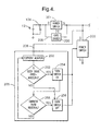
- FIG. 4 illustrates exemplary details regarding gate driver 205, for example. It will be appreciated that the same configuration applies to gate drivers 204, 304 and 305.
- each gate driver includes a current monitor 250 connected, for example, to the drain terminal of FET 202 through circuit branch 206. Decision block 252 allows determining whether the FET 202 is freewheeling or not. In the event FET 202 is freewheeling, FET 202 is turned on at block 254. Conversely, if FET 202 is not freewheeling, then FET 202 would be switched off at block 256. If during freewheeling, current flow reversal is detected, then FET 202 will be turned off at block 256. If no current reversal is detected, the process for monitoring current continues at block 250. It will be appreciated by those skilled in the art, that in lieu of monitoring current, one could monitor voltage to achieve essentially the same operational results described above for controlling operation of the freewheeling FET.
- FET 202 In the step up mode of power conversion (e.g., conversion from 14V to 42V) FET 202 is operated as a PWM switch while FET 201 serves as the freewheeling diode.
- gate driver 204 will synchronously turn on and off FET 201 and prevent conduction of current in the event reversal in the current flow is determined (e.g., determining current flow reversal originally from source to drain to the opposite direction, from drain to source) in FET 201 allowing its body diode to block that current flow.
- a circuit branch 208 connected to the drain terminal of FET 201 allows gate driver 204 to monitor an electrical signal, e.g., voltage and/or current, indicative of the current flow reversal.
- an electrical signal e.g., voltage and/or current
- gate driver 204 will automatically turn off FET 201 and prevent the power sources from shorting to ground.
- block 40 represents one exemplary embodiment of the input/output isolation and protection circuit
- blocks 42 and 44 represent an alternative embodiment for the isolation and protection circuit.
- this circuit utilizes a series combination of power switches configured to prevent power flow through the converter when turned off.
- FETs 101 and 107 comprise the series switches that are controlled by gate drivers 102 and 108, respectively. It will be appreciated that in one exemplary embodiment, gate drivers 102 and 108 in FIG.
- the gate drivers are configured to monitor and control a set of electrical parameters indicative of faulty conditions that would be harmful to the two power sources, the converter, or both.
- the gate drivers respectively monitor the current flow through and the voltages across FETs 101 and 107 in order to prevent excessive power flow, over and under voltages, and reverse polarities from being applied to the two power sources through the converter.
- This circuit in conjunction with the synchronous control circuit will automatically isolate the power sources from any single point converter failure.
- the circuit can be utilized in its active mode for bi-directional charge control and ripple reduction by selectively varying the impedance of the switches.
- the isolation and protection circuit provides independent polarity reversal protection to both power sources.
- the isolation and protection circuit would be to provide the single circuit stage represented by block 40 in FIG. 1 connected to the relatively high voltage power source in lieu of the low voltage power source. It will be appreciated that the designer has the flexibility to choose whichever circuit configuration meets the specific requirements of any given application.
- the present invention can be embodied in the form of computer implemented processes and apparatus for practicing those processes.
- the present invention can also be embodied in the form of computer program code containing computer-readable instructions embodied in tangible media, such as floppy diskettes, CD-ROMs, hard drives, or any other computer-readable storage medium, wherein, when the computer program code is loaded into and executed by a computer, the computer becomes an apparatus for practicing the invention.
- the present invention can also be embodied in the form of computer program code, for example, whether stored in a storage medium, loaded into and/or executed by a computer, or transmitted over some transmission medium, such as over electrical wiring or cabling, through fiber optics, or via electromagnetic radiation, wherein, when the computer program code is loaded into and executed by a computer, the computer becomes an apparatus for practicing the invention.
- the computer program code segments configure the computer to create specific logic circuits or processing modules.
Landscapes
- Engineering & Computer Science (AREA)
- Power Engineering (AREA)
- Dc-Dc Converters (AREA)
- Supply And Distribution Of Alternating Current (AREA)
Abstract
Description
Claims (21)
- A method for bi-directionally controlling power flow between least two separate direct current power (e.g., 12 and 14) sources in a multi-stage power converter system, the method comprising:providing at least first and second power converter stages (e.g., 20 and 30) coupled in parallel circuit to one another;providing a first switching controller (e.g., 113) coupled to selectively actuate a pair of switching devices (e.g., 201 and 202) in the first power converter stage;providing a second switching controller (e.g., 114) coupled to selectively actuate a pair of switching devices (e.g., 301 and 302) in the second power converter stage, with one of the first and second switching controllers selected as a master controller (e.g., 113), and the other one of the first and second switching controllers selected as a slave controller (e.g., 114);determining an average voltage measurement at a respective node (e.g., 601 and 602; or 604 and 606) of each the power converter stages;generating a compensating signal based on the difference of the average voltage measurements at the respective nodes of each of the power converter stages; andapplying the compensating signal to the slave switching controller so that the pair of power switching devices coupled to that slave switching controller is selectively actuated to have a respective on and off duty cycle, the duty cycle imparted by the slave controller being adjustable in response to the compensating signal relative to the duty cycle imparted by the master controller to the pair of power switching devices coupled thereto to avoid current imbalance between the power converter stages.
- The method of claim 1 wherein the first and second switching controllers comprise respective pulse-width modulation controllers.
- The method of claim 2 wherein determining the average voltage measurement at each respective node of the power converter stages comprises coupling a respective averaging filter to receive a voltage signal from each respective node.
- The method of claim 3 wherein generating the compensating signal comprises differentially combining the output signal from each averaging filter to supply a resultant signal, and applying the resultant signal to a compensating circuit configured to generate the compensating signal based on the magnitude and polarity of the resultant signal.
- The method of claim 1 wherein one of the power sources comprises a power source configured to supply a higher voltage relative to the other power source.
- The method of claim 5 wherein one of the power switching devices in each power converter stage is configured to operate in a first mode of power conversion in pulse-width modulation switching condition, and the other one of the power switching devices is configured to operate, at least part of the time, in a freewheeling condition, and wherein in a second power conversion mode the one power switching device is configured to operate, at least part of the time, in the freewheeling condition, and the other power switching device is configured to operate in the pulse-width modulation switching condition.
- The method of claim 6 wherein the first mode of power conversion comprises a step-up mode of power conversion, and the second mode of power conversion comprises a step-down mode of power conversion.
- The method of claim 7 further comprising monitoring a predefined electrical parameter indicative of current passing in a first direction through the freewheeling device and setting that device to an on-state during the freewheeling condition, and to an off-state when current flow reversal relative to that first direction is determined for that switching device.
- The method of claim 1 further comprising coupling to at least one of the power sources a circuit comprising a pair of power switching devices connected in series circuit and configured to bi-directionally isolate and protect the converter and/or power source under predefined fault conditions.
- The method of claim 1 further comprising coupling to each of the power sources a circuit comprising a respective power switching device configured to bi-directionally isolate and protect the converter and/or power sources under predefined fault conditions.
- A multi-stage power converter system for bi-directionally controlling power flow between at least two separate direct current power sources (e.g., 12 and 14), the power converter system comprising:at least first and second power converter stages (e.g., 20 and 30) coupled in parallel circuit to one another;a first switching controller (e.g., 113) coupled to selectively actuate a pair of switching devices in the first power converter stage;a second switching controller (e.g., 114) coupled to selectively actuate a pair of switching devices in the second power converter stage, with one of the first and second switching controllers selected as a master controller (e.g,. 113), and the other one of the first and second switching controllers selected as a slave controller (e.g., 114);a feedback controller (e.g., 110) configured to avoid current imbalance between the power converter stages by:determining an average voltage measurement at a respective node of each the power converter stages;generating a compensating signal based on the difference of the average voltage measurements at the respective nodes of each of the power converter stages; andapplying the compensating signal to the slave switching controller so that the pair of power switching devices coupled to that slave switching controller is selectively actuated to have a respective on and off duty cycle, the duty cycle imparted by the slave controller being adjustable in response to the compensating signal relative to the duty cycle imparted by the master controller to the pair of power switching devices coupled thereto, thus avoiding current imbalance between the power converter stages.
- The power converter system of claim 11 wherein the first and second switching controllers comprise respective pulse-width modulation controllers.
- The power converter system of claim 12 further comprising a respective averaging filter coupled to receive a voltage signal from each respective node, each filter (120 and 122) configured to determine the average voltage measurement at each respective node of the power converter stages.
- The power converter system of claim 13 further comprising a signal combiner (e.g., 124) configured to differentially combine the output signal from each averaging filter to supply a resultant signal, the signal combiner coupled to apply the resultant signal to a compensating circuit (e.g., 128) configured to generate the compensating signal based on the magnitude and polarity of the resultant signal.
- The power converter system of claim 11 wherein one of the power sources comprises a power source configured to supply a higher voltage relative to the other power source.
- The power converter system of claim 15 wherein one of the power switching devices in each power converter stage is configured to operate in a first mode of power conversion in pulse-width modulation switching condition, and the other one of the power switching devices is configured to operate, at least part of the time, in a freewheeling condition, and wherein in a second power conversion mode the one power switching device is configured to operate, at least part of the time, in the freewheeling condition, and the other power switching device is configured to operate in the pulse-width modulation switching condition.
- The power converter system of claim 16 wherein the first mode of power conversion comprises a step-up mode of power conversion, and the second mode of power conversion comprises a step-down mode of power conversion.
- The power converter system of claim 17 further comprising a circuit (e.g., 250) configured to monitor a predefined electrical parameter indicative of current passing in a first direction through the freewheeling device, the circuit further configured to set that device to an on-state during the freewheeling condition, and to an off-state when current flow reversal relative to that first direction is determined for that switching device.
- The power converter system of claim 11 further comprising a circuit (e.g., 40) coupled to at least one of the power sources and including a pair of power switching devices connected in series circuit and configured to bi-directionally isolate and protect the converter and/or power source under predefined fault conditions.
- The power converter system of claim 11 further comprising a circuit having respective circuit stages (e.g., 42 and 44) coupled to a respective one of the power sources, each circuit stage including a respective power switching device and, in combination, configured to bi-directionally isolate and protect the converter and/or power sources under predefined fault conditions.
- A multi-stage power converter system for bi-directionally controlling power flow between at least two separate direct current power sources (e.g., 12 and 14), the power converter system comprising:at least first and second power converter stages (e.g., 20 and 30)coupled in parallel circuit to one another;a first switching controller (e.g., 113) coupled to selectively actuate a pair of switching devices in the first power converter stage;a second switching controller (e.g., 114) coupled to selectively actuate a pair of switching devices in the second power converter stage, with one of the first and second switching controllers selected as a master controller, and the other one of the first and second switching controllers selected as a slave controller;a feedback controller (e.g., 110) configured to avoid current imbalance between the power converter stages, the feedback controller comprising:a circuit (e.g., 120 and 122) configured to determine an average voltage measurement at a respective node of each the power converter stages;a compensator (e.g., 128) configured to generate a compensating signal based on the difference of the average voltage measurements at the respective nodes of each of the power converter stages, the compensator being coupled to the slave switching controller to supply the compensating signal thereto so that the pair of power switching devices coupled to that slave switching controller is selectively actuated to have a respective on and off duty cycle, the duty cycle imparted by the slave controller being adjustable in response to the compensating signal relative to the duty cycle imparted by the master controller to the pair of power switching devices coupled thereto, thus avoiding current imbalance between the power converter stages.
Applications Claiming Priority (2)
| Application Number | Priority Date | Filing Date | Title |
|---|---|---|---|
| US10/012,836 US6437462B1 (en) | 2001-12-10 | 2001-12-10 | Bi-directional DC/DC converter and control method therefor |
| US12836 | 2001-12-10 |
Publications (2)
| Publication Number | Publication Date |
|---|---|
| EP1318592A2 true EP1318592A2 (en) | 2003-06-11 |
| EP1318592A3 EP1318592A3 (en) | 2005-03-23 |
Family
ID=21756943
Family Applications (1)
| Application Number | Title | Priority Date | Filing Date |
|---|---|---|---|
| EP02079897A Withdrawn EP1318592A3 (en) | 2001-12-10 | 2002-11-25 | Bi-directional dc/dc converter and control method therefor |
Country Status (2)
| Country | Link |
|---|---|
| US (1) | US6437462B1 (en) |
| EP (1) | EP1318592A3 (en) |
Cited By (2)
| Publication number | Priority date | Publication date | Assignee | Title |
|---|---|---|---|---|
| DE102007058681A1 (en) * | 2007-12-06 | 2009-06-10 | Siemens Ag | Step up and step down controller, particularly for feeding, for use with half bridge and full bridge for converting direct current voltage into output direct current voltage, has fuel cells in electrical network |
| CN104704698A (en) * | 2012-10-17 | 2015-06-10 | 罗伯特·博世有限公司 | Protective circuit arrangement for multi-voltage grid |
Families Citing this family (21)
| Publication number | Priority date | Publication date | Assignee | Title |
|---|---|---|---|---|
| JP3706814B2 (en) * | 2001-06-07 | 2005-10-19 | 株式会社ルネサステクノロジ | DC-DC converter and control method of DC-DC converter |
| US7026800B2 (en) * | 2002-10-17 | 2006-04-11 | Richtek Technology Corp. | Feed-forward method for improving a transient response for a DC—DC power conversion and DC—DC voltage converter utilizing the same |
| JP2004159410A (en) * | 2002-11-06 | 2004-06-03 | Pioneer Electronic Corp | Power supply device and power supply control method |
| DE50311044D1 (en) | 2003-02-27 | 2009-02-26 | Delphi Tech Inc | Electronic protection circuit |
| EP1548921A1 (en) * | 2003-12-23 | 2005-06-29 | Alcatel | Dc-to-dc converter for a car electrical system |
| DE102004018261B4 (en) * | 2004-04-15 | 2006-12-14 | Infineon Technologies Ag | Power supply system for electrical consumers in vehicles |
| JP4254658B2 (en) * | 2004-08-23 | 2009-04-15 | 株式会社デンソー | In-vehicle power supply system |
| JP4449940B2 (en) * | 2006-05-16 | 2010-04-14 | トヨタ自動車株式会社 | Dual power supply system for vehicles |
| DE102007010819B4 (en) * | 2007-03-06 | 2010-10-14 | Audi Ag | DC-DC converter system with current symetry circuit and method for balancing the phase currents for a multi-phase DC-DC converter system |
| US7932641B2 (en) * | 2007-06-11 | 2011-04-26 | International Business Machines Corporation | Low voltage head room detection for reliable start-up of self-biased analog circuits |
| EP2460256B1 (en) * | 2009-07-31 | 2017-11-15 | Thermo King Corporation | Bi-directional battery voltage converter |
| JP4783453B2 (en) * | 2009-09-10 | 2011-09-28 | 力也 阿部 | Multi-terminal type asynchronous interconnection device, power equipment control terminal device, power network system and control method therefor |
| DE102011086829A1 (en) * | 2011-11-22 | 2013-05-23 | Continental Automotive Gmbh | On-board network and method for operating a vehicle electrical system |
| DE102012106261A1 (en) | 2012-07-12 | 2014-01-16 | Hella Kgaa Hueck & Co. | DC-DC converter circuitry |
| CN104348225B (en) * | 2014-08-12 | 2017-07-11 | 矽力杰半导体技术(杭州)有限公司 | A kind of battery charge-discharge circuit of Single switch and the control method of battery charging and discharging |
| US9425691B1 (en) * | 2015-06-17 | 2016-08-23 | Cypress Semiconductor Corporation | Low thermal design for DC-DC converter |
| NZ760094A (en) * | 2017-05-15 | 2021-07-30 | Dynapower Co Llc | Dc/dc converter and control thereof |
| JP6984244B2 (en) * | 2017-09-04 | 2021-12-17 | トヨタ自動車株式会社 | Power system |
| US11251741B2 (en) * | 2018-11-15 | 2022-02-15 | Eaton Intelligent Power Limited | Modular board-level motor control system with integrated protection and control components |
| CN109861532B (en) * | 2019-03-01 | 2024-05-03 | 中国第一汽车股份有限公司 | A DC/DC converter and a vehicle control method based thereon |
| WO2021257433A1 (en) * | 2020-06-17 | 2021-12-23 | Milwaukee Electric Tool Corporation | Motor control for gas engine replacement device |
Family Cites Families (8)
| Publication number | Priority date | Publication date | Assignee | Title |
|---|---|---|---|---|
| US4359679A (en) * | 1978-01-16 | 1982-11-16 | Wescom Switching, Inc. | Switching d-c. regulator and load-sharing system for multiple regulators |
| US4736151A (en) * | 1986-12-23 | 1988-04-05 | Sundstrand Corporation | Bi-directional buck/boost DC/DC converter |
| US5157269A (en) * | 1991-01-31 | 1992-10-20 | Unitrode Corporation | Load current sharing circuit |
| DE19645944A1 (en) * | 1996-11-07 | 1998-05-14 | Bosch Gmbh Robert | Control unit for an electrical system |
| EP1061629B1 (en) * | 1999-06-07 | 2004-08-25 | STMicroelectronics S.r.l. | Single wire current sharing control technique for parallel/redundant operation of a plurality of PWM converters |
| GB2357641B (en) * | 1999-12-20 | 2002-02-20 | Motorola Ltd | DC-DC Converter and energy management system |
| US6285571B1 (en) * | 2000-03-03 | 2001-09-04 | Linfinity Microelectronics | Method and apparatus for an efficient multiphase switching regulator |
| US6304068B1 (en) * | 2000-04-20 | 2001-10-16 | City University Of Hong Kong | Bi-directional switched-capacitor based voltage converter |
-
2001
- 2001-12-10 US US10/012,836 patent/US6437462B1/en not_active Expired - Lifetime
-
2002
- 2002-11-25 EP EP02079897A patent/EP1318592A3/en not_active Withdrawn
Cited By (3)
| Publication number | Priority date | Publication date | Assignee | Title |
|---|---|---|---|---|
| DE102007058681A1 (en) * | 2007-12-06 | 2009-06-10 | Siemens Ag | Step up and step down controller, particularly for feeding, for use with half bridge and full bridge for converting direct current voltage into output direct current voltage, has fuel cells in electrical network |
| CN104704698A (en) * | 2012-10-17 | 2015-06-10 | 罗伯特·博世有限公司 | Protective circuit arrangement for multi-voltage grid |
| CN104704698B (en) * | 2012-10-17 | 2018-05-04 | 罗伯特·博世有限公司 | Protective circuit arrangement for multi-voltage grid |
Also Published As
| Publication number | Publication date |
|---|---|
| US6437462B1 (en) | 2002-08-20 |
| EP1318592A3 (en) | 2005-03-23 |
Similar Documents
| Publication | Publication Date | Title |
|---|---|---|
| US6437462B1 (en) | Bi-directional DC/DC converter and control method therefor | |
| US11084438B2 (en) | Power supply apparatus for vehicles | |
| US9601984B2 (en) | Power converter | |
| US9438115B2 (en) | Power supply system | |
| EP2398146B1 (en) | High power DC SSPC with capability of soft turn-on to large capacitive loads | |
| US7830036B2 (en) | Power electronic module pre-charge system and method | |
| EP2978118B1 (en) | Power converter and power conditioner | |
| US20100164446A1 (en) | Bidirectional dc-dc converter | |
| US9893511B2 (en) | Protective circuit assemblage for a multi-voltage electrical system | |
| US11424670B2 (en) | Drive device for switch | |
| KR101734210B1 (en) | Bidirectional dc-dc converter | |
| US11728802B2 (en) | Drive circuit | |
| US11545887B2 (en) | Safety cutoff circuit for power converter | |
| US20190353715A1 (en) | Failure detection device for onboard power supply device, and onboard power supply device | |
| JP4209196B2 (en) | Power converter | |
| US11990826B2 (en) | Power electronics device and method for supplying electrical voltage to a driver circuit of a power semiconductor switch | |
| US10906484B2 (en) | In-vehicle power supply device | |
| US11012021B2 (en) | Inverter device and control circuit therefor, and motor driving system | |
| US11476750B2 (en) | Vehicle power supply device with charge circuit section | |
| CN113054846A (en) | Control device for power conversion device | |
| JP3445649B2 (en) | Inverter device | |
| US9225323B1 (en) | Signal crossing detection | |
| WO2020175078A1 (en) | Double step-down chopper circuit | |
| JP7641175B2 (en) | Power supply system and control method thereof | |
| EP4550647A1 (en) | Power converters and methods of controlling a power converter |
Legal Events
| Date | Code | Title | Description |
|---|---|---|---|
| PUAI | Public reference made under article 153(3) epc to a published international application that has entered the european phase |
Free format text: ORIGINAL CODE: 0009012 |
|
| AK | Designated contracting states |
Designated state(s): AT BE BG CH CY CZ DE DK EE ES FI FR GB GR IE IT LI LU MC NL PT SE SK TR |
|
| AX | Request for extension of the european patent |
Extension state: AL LT LV MK RO SI |
|
| PUAL | Search report despatched |
Free format text: ORIGINAL CODE: 0009013 |
|
| AK | Designated contracting states |
Kind code of ref document: A3 Designated state(s): AT BE BG CH CY CZ DE DK EE ES FI FR GB GR IE IT LI LU MC NL PT SE SK TR |
|
| AX | Request for extension of the european patent |
Extension state: AL LT LV MK RO SI |
|
| STAA | Information on the status of an ep patent application or granted ep patent |
Free format text: STATUS: THE APPLICATION IS DEEMED TO BE WITHDRAWN |
|
| AKX | Designation fees paid | ||
| 18D | Application deemed to be withdrawn |
Effective date: 20050531 |
|
| REG | Reference to a national code |
Ref country code: DE Ref legal event code: 8566 |