EP1318208A2 - Method of depositing heusler alloy thin film by co-sputtering - Google Patents
Method of depositing heusler alloy thin film by co-sputtering Download PDFInfo
- Publication number
- EP1318208A2 EP1318208A2 EP02255286A EP02255286A EP1318208A2 EP 1318208 A2 EP1318208 A2 EP 1318208A2 EP 02255286 A EP02255286 A EP 02255286A EP 02255286 A EP02255286 A EP 02255286A EP 1318208 A2 EP1318208 A2 EP 1318208A2
- Authority
- EP
- European Patent Office
- Prior art keywords
- thin film
- heusler alloy
- alloy thin
- substrate
- sputtering
- Prior art date
- Legal status (The legal status is an assumption and is not a legal conclusion. Google has not performed a legal analysis and makes no representation as to the accuracy of the status listed.)
- Withdrawn
Links
Images



Classifications
-
- G—PHYSICS
- G11—INFORMATION STORAGE
- G11B—INFORMATION STORAGE BASED ON RELATIVE MOVEMENT BETWEEN RECORD CARRIER AND TRANSDUCER
- G11B5/00—Recording by magnetisation or demagnetisation of a record carrier; Reproducing by magnetic means; Record carriers therefor
- G11B5/84—Processes or apparatus specially adapted for manufacturing record carriers
- G11B5/851—Coating a support with a magnetic layer by sputtering
-
- C—CHEMISTRY; METALLURGY
- C23—COATING METALLIC MATERIAL; COATING MATERIAL WITH METALLIC MATERIAL; CHEMICAL SURFACE TREATMENT; DIFFUSION TREATMENT OF METALLIC MATERIAL; COATING BY VACUUM EVAPORATION, BY SPUTTERING, BY ION IMPLANTATION OR BY CHEMICAL VAPOUR DEPOSITION, IN GENERAL; INHIBITING CORROSION OF METALLIC MATERIAL OR INCRUSTATION IN GENERAL
- C23C—COATING METALLIC MATERIAL; COATING MATERIAL WITH METALLIC MATERIAL; SURFACE TREATMENT OF METALLIC MATERIAL BY DIFFUSION INTO THE SURFACE, BY CHEMICAL CONVERSION OR SUBSTITUTION; COATING BY VACUUM EVAPORATION, BY SPUTTERING, BY ION IMPLANTATION OR BY CHEMICAL VAPOUR DEPOSITION, IN GENERAL
- C23C14/00—Coating by vacuum evaporation, by sputtering or by ion implantation of the coating forming material
- C23C14/06—Coating by vacuum evaporation, by sputtering or by ion implantation of the coating forming material characterised by the coating material
- C23C14/14—Metallic material, boron or silicon
-
- C—CHEMISTRY; METALLURGY
- C23—COATING METALLIC MATERIAL; COATING MATERIAL WITH METALLIC MATERIAL; CHEMICAL SURFACE TREATMENT; DIFFUSION TREATMENT OF METALLIC MATERIAL; COATING BY VACUUM EVAPORATION, BY SPUTTERING, BY ION IMPLANTATION OR BY CHEMICAL VAPOUR DEPOSITION, IN GENERAL; INHIBITING CORROSION OF METALLIC MATERIAL OR INCRUSTATION IN GENERAL
- C23C—COATING METALLIC MATERIAL; COATING MATERIAL WITH METALLIC MATERIAL; SURFACE TREATMENT OF METALLIC MATERIAL BY DIFFUSION INTO THE SURFACE, BY CHEMICAL CONVERSION OR SUBSTITUTION; COATING BY VACUUM EVAPORATION, BY SPUTTERING, BY ION IMPLANTATION OR BY CHEMICAL VAPOUR DEPOSITION, IN GENERAL
- C23C14/00—Coating by vacuum evaporation, by sputtering or by ion implantation of the coating forming material
- C23C14/22—Coating by vacuum evaporation, by sputtering or by ion implantation of the coating forming material characterised by the process of coating
- C23C14/34—Sputtering
- C23C14/3464—Sputtering using more than one target
-
- C—CHEMISTRY; METALLURGY
- C23—COATING METALLIC MATERIAL; COATING MATERIAL WITH METALLIC MATERIAL; CHEMICAL SURFACE TREATMENT; DIFFUSION TREATMENT OF METALLIC MATERIAL; COATING BY VACUUM EVAPORATION, BY SPUTTERING, BY ION IMPLANTATION OR BY CHEMICAL VAPOUR DEPOSITION, IN GENERAL; INHIBITING CORROSION OF METALLIC MATERIAL OR INCRUSTATION IN GENERAL
- C23C—COATING METALLIC MATERIAL; COATING MATERIAL WITH METALLIC MATERIAL; SURFACE TREATMENT OF METALLIC MATERIAL BY DIFFUSION INTO THE SURFACE, BY CHEMICAL CONVERSION OR SUBSTITUTION; COATING BY VACUUM EVAPORATION, BY SPUTTERING, BY ION IMPLANTATION OR BY CHEMICAL VAPOUR DEPOSITION, IN GENERAL
- C23C14/00—Coating by vacuum evaporation, by sputtering or by ion implantation of the coating forming material
- C23C14/22—Coating by vacuum evaporation, by sputtering or by ion implantation of the coating forming material characterised by the process of coating
- C23C14/54—Controlling or regulating the coating process
- C23C14/541—Heating or cooling of the substrates
-
- C—CHEMISTRY; METALLURGY
- C30—CRYSTAL GROWTH
- C30B—SINGLE-CRYSTAL GROWTH; UNIDIRECTIONAL SOLIDIFICATION OF EUTECTIC MATERIAL OR UNIDIRECTIONAL DEMIXING OF EUTECTOID MATERIAL; REFINING BY ZONE-MELTING OF MATERIAL; PRODUCTION OF A HOMOGENEOUS POLYCRYSTALLINE MATERIAL WITH DEFINED STRUCTURE; SINGLE CRYSTALS OR HOMOGENEOUS POLYCRYSTALLINE MATERIAL WITH DEFINED STRUCTURE; AFTER-TREATMENT OF SINGLE CRYSTALS OR A HOMOGENEOUS POLYCRYSTALLINE MATERIAL WITH DEFINED STRUCTURE; APPARATUS THEREFOR
- C30B23/00—Single-crystal growth by condensing evaporated or sublimed materials
- C30B23/02—Epitaxial-layer growth
-
- C—CHEMISTRY; METALLURGY
- C30—CRYSTAL GROWTH
- C30B—SINGLE-CRYSTAL GROWTH; UNIDIRECTIONAL SOLIDIFICATION OF EUTECTIC MATERIAL OR UNIDIRECTIONAL DEMIXING OF EUTECTOID MATERIAL; REFINING BY ZONE-MELTING OF MATERIAL; PRODUCTION OF A HOMOGENEOUS POLYCRYSTALLINE MATERIAL WITH DEFINED STRUCTURE; SINGLE CRYSTALS OR HOMOGENEOUS POLYCRYSTALLINE MATERIAL WITH DEFINED STRUCTURE; AFTER-TREATMENT OF SINGLE CRYSTALS OR A HOMOGENEOUS POLYCRYSTALLINE MATERIAL WITH DEFINED STRUCTURE; APPARATUS THEREFOR
- C30B29/00—Single crystals or homogeneous polycrystalline material with defined structure characterised by the material or by their shape
- C30B29/10—Inorganic compounds or compositions
- C30B29/52—Alloys
Definitions
- the present invention relates to a method of depositing a Heusler alloy thin film, and more particularly, to a method of forming a Heusler alloy thin film having a more improved property by depositing materials constituting the Heusler alloy thin film by co-sputtering at the same time.
- a magnetic random access memory is one of nonvolatile memory devices, which is a solid magnetic memory using a magnetoresistance effect based on a particular spin dependence conduction phenomenon of a nano magnetic.
- This MRAM uses a giant magnetoresistance phenomenon which occurs because a spin that is degree of freedom of electrons has a great effect on an electron transmission, or a tunnel magnetoresistance phenomenon.
- the giant magnetoresistance refers to a phenomenon in which differences in resistance occur when the spin between ferromagnetic substances in an arrangement of ferromagnetic substance/metal nonmagnetic substance/ferromagnetic substance is equally and oppositely arranged.
- the tunnel magnetoresitance refers to a phenomenon in which transmission of current is easier when the spin is equally arranged on two ferromagnetic layers in an arrangement of ferromagnetic substance/insulator/ferromagnetic substance than when the spins is oppositely arranged.
- the difference in resistance values due to magnetization directions is relatively small and thus the difference in voltage values cannot be great.
- the size of a MOSFET which is combined with a GMR layer to constitute a cell has to be large. Thus, a study on practical use of the MRAM using a TMR layer has been more active.
- Heusler alloy is deposited by sputtering, using molecular beam epitaxy (MBE) or in a state that a chip is placed on a target.
- MBE molecular beam epitaxy
- this conventional method of manufacturing a Huesler alloy thin film is inefficient due to difficulties in productivity and problems relating to control of the composition.
- the efficiency of sputtering is widely accepted when depositing a general alloy thin film.
- Heusleralloy has a fragile characteristic and thus it is difficult to manufacture Heusler alloy as targets.
- components of the Heusler alloy thin film are placed on the target bracket as one of single targets and binary alloy targets.
- the substrate holder is preferably maintained at a temperature of about 200 - 500°C.
- the chamber is preferably maintained in a vacuum of 10 -2 - 10 -3 Torr.
- each of components constituting the Heusler alloy thin film is sputtered as a single target.
- a general structure formula of Heusler alloy is X2YZ.
- X is a metal such as Co or Cu
- Y is Mn
- Z is a nonmagnetic substance such as Al, Si, Ga, Ge, Sn, or Sb of a 3A group or 4A group.
- semi-Heusleralloy such as PtMnSb or NiMnSb having a structure formula of XYZ.
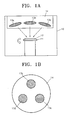
- FIG. 1A is a schematic cross-sectional view of a sputtering system used in a process of manufacturing a Heusleralloy thin film by co-sputtering according to the present invention.
- FIG. 1 B is a plan view of each single target that is components constituting a Heusleralloy thin film and placed on a target bracket.
- Components constituting a Heusleralloy thin film e.g., Cu, Mn, Al targets 13a, 13b, and 13c, are placed on a target bracket 14 in a chamber 10 of a sputtering system.
- a CuMnAI alloy is deposited on a substrate 11 after deposition conditions are set based on the components.
- the CuMnAI alloy may be formed of one of binary alloys such as CuMn, CuAl, or MnAI and one of Cu, Mn, and Al.
- a general sputtering apparatus and a discharging gas may be used with controlling deposition rate.
- single targets 13a, 13b, and 13c constituting a Heusler alloy thin film are deposited on a target bracket 14.
- a substrate 12 is placed on a substrate holder 11.
- the inside of a chamber 10 of the sputtering system is maintained in a predetermined vacuum.
- Such inside vacuum is generally about 7 ⁇ 10 -10 Torr.
- a discharging gas, e.g., Ar, is supplied into the chamber 10.
- vacuum is within a range of 10 -3 ⁇ 10 -2 Torr.
- a vacuum pump and a discharging gas supply apparatus operate to maintain a predetermined vacuum.
- the substrate 12 is maintained at a temperature of about 200 - 500 °C, and the substrate holder 11 rotates at a predetermined speed.
- the distance between the substrate 12 and the targets 13a, 13b, and 13c may depend on kinds of sputtering systems, and is generally within and without a range of 5 - 20 cm. This process is the same as a general sputtering process.
- a voltage is applied between the substrate holder 11 and the target bracket 14 to make the discharging gas into plasma.
- components constituting the Heusleralloy thin film are deposited on the substrate 12.
- deposition rate of Cu is 83 ⁇ /min
- deposition rate of Mn is 44 ⁇ /min
- deposition rate of Al is 57 ⁇ /min.
- a Heusleralloy thin film having excellent characteristics can be formed if deposition rates of components of the Heusler alloy thin film are low. This may depend on kinds of sputtering systems.
- FIGS. 2A through 2D are graphs showing magnetic characteristics of a Heusler alloy thin film manufactured by co-sputtering based on changes in temperature of a substrate, which are measured using a VSM apparatus, according to the present invention.
- a Heusler thin film is deposited on a substrate having a temperature of about 200°C for about 20 minutes.
- the Heusleralloy thin film does not have magnetic characteristics which may be used in a MRAM.
- FIG. 2B a Heusleralloy thin film is deposited on a substrate having a temperature of about 250°C for about 20 minutes.
- the Heusler alloy thin film have distinct magnetic characteristics and a considerably increased magnetization value compared to the Heusleralloy thin film deposited at the temperature of about 200°C.
- a Heusleralloy thin film is deposited on a substrate having a temperature of about 300°C for about 20 minutes.
- the Heusler alloy thin film has a greater magnetization value than the Heusler alloy thin film in FIG. 2B.
- a Heusler alloy thin film is deposited on a substrate having a temperature of about 400°C for about 20 minutes. It can be seen that the Heusler alloy thin film has the most increased saturation magnetization value.
- the distance between the substrate and targets in the deposition of the Heusler alloy thin film is about 10cm. Only temperature of the substrate varies and other conditions are the same when depositing each Heusler alloy thin film. Thus, the Heusler alloy thin films deposited on the substrates are the same.
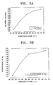
- FIGS. 3A and 3B are graphs showing Ms/Area values and Mr/Ms values of a Heusler alloy thin film based on temperature of a substrate according to the present invention.
- Ms values represent saturation magnetization values
- Mr values represent remaining magnetization values
- Area represents the area of a substrate.
- FIG. 4 is a graph showing X-ray diffraction measured with respect to a Heusler alloy thin film manufactured by changing a substrate temperature according to the present invention. Characteristics of a Hesuler alloy thin film based on a process temperature will be described in more detail with reference to FIG. 4.
- peaks occurring near to about 33, 62, and 68° represent characteristic peaks of a silicon substrate. Peak occurring near to about 26° represents superlattice peak. Peak occurring near to about 42° represents peak showing that components in a crystal structure of Heusler alloy are disordered.
- intensity values when a substrate temperature is 250, 300, and 400°C, respectively, are transferred by a 100 unit in a y-axis direction for easy comparison.
- intensity values in a base section except for characteristic peaks are almost the same.
- supperlattic peak occurs, it is known that the Heusler alloy thin film has excellent characteristics as a magnetic thin film.
- supperlattice peak near to about 26° stands out as the temperature of the substrate increases and peak near to about 42° showing disorder of the crystal structure of the Heusler thin film decreases.
- a Heusler alloy thin film having excellent magnetic characteristics it is easy to manufacture a Heusler alloy thin film having excellent magnetic characteristics.
- a co-sputtering deposition method can easily vary depending on changes in components constituting the Heusler alloy thin film and composition.
- the Heusler alloy thin film can obtain characteristics such as a high MR rate and thus is easily adopted in the manufacture of a MRAM.
- a MRAM having an excellent efficiency can be provided. Uniformity tolerance, reliability, and yield can be improved in the manufacture of the MRAM.
- a signal-to-noise (S/N) ratio and sensing margin increase and a reduction in the MR rate occurring due to a bias voltage dependence degree of the MR rate can decrease.
Landscapes
- Chemical & Material Sciences (AREA)
- Engineering & Computer Science (AREA)
- Materials Engineering (AREA)
- Metallurgy (AREA)
- Organic Chemistry (AREA)
- Chemical Kinetics & Catalysis (AREA)
- Mechanical Engineering (AREA)
- Crystallography & Structural Chemistry (AREA)
- Inorganic Chemistry (AREA)
- Thin Magnetic Films (AREA)
- Hall/Mr Elements (AREA)
- Physical Vapour Deposition (AREA)
Abstract
Description
Claims (6)
- A method of manufacturing a Heusler alloy thin film having one of structure formulae X2YZ and XYZ by co-sputtering using a deposition apparatus having a substrate placed on a substrate holder in a chamber and targets positioned on a target bracket spaced apart from the substrate,
wherein components of the Heusler alloy thin film are placed on the target bracket as one of single targets and binary alloy targets. - The method of claim 1, wherein the substrate holder is maintained at a temperature of 200 - 500°C.
- The method of claim 1 or 2, wherein the chamber is maintained in a vacuum of 10-2 -10-3 Torr.
- The method of any of claims 1 to 3, wherein the distance between the substrate and the targets is within a range of 5 - 20 cm.
- The method of any of claims 1 to 4, wherein in the structure formula X2YZ of the Heusler alloy thin film, X is one of Co, Cu, Ni, Fe-based metals; Y is Mn or Ti, and Z is one of Al, Si, Ga, Ge, Sn, and Sb that is a nonmagnetic material of one of 3A and 4A groups of the Periodic Table.
- The method of any of claims 1 to 4, wherein the structure formula XYZ of the Heusler alloy thin film is one of PtMnSb and NiMnSb.
Applications Claiming Priority (2)
| Application Number | Priority Date | Filing Date | Title |
|---|---|---|---|
| KR2001077421 | 2001-12-07 | ||
| KR1020010077421A KR20030047046A (en) | 2001-12-07 | 2001-12-07 | Deposition of Heusler alloy thin film by Co-sputtering |
Publications (2)
| Publication Number | Publication Date |
|---|---|
| EP1318208A2 true EP1318208A2 (en) | 2003-06-11 |
| EP1318208A3 EP1318208A3 (en) | 2003-07-02 |
Family
ID=19716782
Family Applications (1)
| Application Number | Title | Priority Date | Filing Date |
|---|---|---|---|
| EP02255286A Withdrawn EP1318208A3 (en) | 2001-12-07 | 2002-07-29 | Method of depositing heusler alloy thin film by co-sputtering |
Country Status (4)
| Country | Link |
|---|---|
| US (1) | US20030116426A1 (en) |
| EP (1) | EP1318208A3 (en) |
| JP (1) | JP2003277926A (en) |
| KR (1) | KR20030047046A (en) |
Cited By (3)
| Publication number | Priority date | Publication date | Assignee | Title |
|---|---|---|---|---|
| FR2905707A1 (en) * | 2006-09-08 | 2008-03-14 | Centre Nat Rech Scient | PROCESS FOR DEPOSITING ON A SUBSTRATE A THIN LAYER OF METAL ALLOY AND METAL ALLOY IN THE FORM OF A THIN LAYER. |
| US7533456B2 (en) | 2006-08-30 | 2009-05-19 | Tdk Corporation | Fabrication process for magneto-resistive effect devices of the CPP structure |
| EP1947205A3 (en) * | 2007-01-19 | 2010-09-22 | Heraeus, Inc. | Low oxygen content, crack-free heusler and heusler-like alloys & deposition sources & methods of making same |
Families Citing this family (7)
| Publication number | Priority date | Publication date | Assignee | Title |
|---|---|---|---|---|
| JP2005228998A (en) * | 2004-02-13 | 2005-08-25 | Japan Science & Technology Agency | Magnetic thin film, magnetoresistive effect element and magnetic device using the same |
| US7672088B2 (en) * | 2006-06-21 | 2010-03-02 | Headway Technologies, Inc. | Heusler alloy with insertion layer to reduce the ordering temperature for CPP, TMR, MRAM, and other spintronics applications |
| US7957106B2 (en) * | 2007-04-30 | 2011-06-07 | Hitachi Global Storage Technologies Netherlands, B.V. | Chemically disordered material used to form a free layer or a pinned layer of a magnetoresistance (MR) read element |
| CN102129863B (en) * | 2010-12-17 | 2013-04-03 | 北京科技大学 | Spin valve structure with electric field-adjustable magnetoresistance and preparation process thereof |
| JP2016134520A (en) * | 2015-01-20 | 2016-07-25 | 国立研究開発法人物質・材料研究機構 | Heusler alloy thin film and manufacturing method thereof, magnetoresistive effect element, magnetic memory |
| US10818839B2 (en) | 2018-03-15 | 2020-10-27 | Samsung Electronics Co., Ltd. | Apparatus for and method of fabricating semiconductor devices |
| CN114093663A (en) * | 2021-12-03 | 2022-02-25 | 天津城建大学 | Room temperature magnetocaloric material and preparation method thereof |
Family Cites Families (5)
| Publication number | Priority date | Publication date | Assignee | Title |
|---|---|---|---|---|
| JPH0661087A (en) * | 1985-06-11 | 1994-03-04 | Nikon Corp | Method of manufacturing magnetic thin film |
| JPS63285739A (en) * | 1987-05-18 | 1988-11-22 | Kureha Chem Ind Co Ltd | Production of thin film for magneto-optical recording and reproduction |
| US4952295A (en) * | 1988-04-15 | 1990-08-28 | Matsushita Electric Industrial Co., Ltd. | Method of producing a deposition film of composite material |
| US5525199A (en) * | 1991-11-13 | 1996-06-11 | Optical Corporation Of America | Low pressure reactive magnetron sputtering apparatus and method |
| JP3629057B2 (en) * | 1995-03-14 | 2005-03-16 | 株式会社東芝 | Method for manufacturing Heusler alloy thin film, laminated film provided with magnetic film, magnetoresistive effect element and solid-state magnetic recording element using the same |
-
2001
- 2001-12-07 KR KR1020010077421A patent/KR20030047046A/en not_active Ceased
-
2002
- 2002-07-29 EP EP02255286A patent/EP1318208A3/en not_active Withdrawn
- 2002-11-08 JP JP2002324566A patent/JP2003277926A/en not_active Withdrawn
- 2002-12-04 US US10/309,212 patent/US20030116426A1/en not_active Abandoned
Cited By (4)
| Publication number | Priority date | Publication date | Assignee | Title |
|---|---|---|---|---|
| US7533456B2 (en) | 2006-08-30 | 2009-05-19 | Tdk Corporation | Fabrication process for magneto-resistive effect devices of the CPP structure |
| FR2905707A1 (en) * | 2006-09-08 | 2008-03-14 | Centre Nat Rech Scient | PROCESS FOR DEPOSITING ON A SUBSTRATE A THIN LAYER OF METAL ALLOY AND METAL ALLOY IN THE FORM OF A THIN LAYER. |
| WO2008028981A3 (en) * | 2006-09-08 | 2008-07-31 | Centre Nat Rech Scient | Process for depositing a thin film of a metal alloy on a substrate, and a metal alloy in thin-film form |
| EP1947205A3 (en) * | 2007-01-19 | 2010-09-22 | Heraeus, Inc. | Low oxygen content, crack-free heusler and heusler-like alloys & deposition sources & methods of making same |
Also Published As
| Publication number | Publication date |
|---|---|
| JP2003277926A (en) | 2003-10-02 |
| US20030116426A1 (en) | 2003-06-26 |
| KR20030047046A (en) | 2003-06-18 |
| EP1318208A3 (en) | 2003-07-02 |
Similar Documents
| Publication | Publication Date | Title |
|---|---|---|
| KR101242628B1 (en) | FERROMAGNETIC PREFERRED GRAIN GROWTH PROMOTION SEED LAYER FOR AMORPHOUS OR MICROCRYSTALLINE MgO TUNNEL BARRIER | |
| US8318510B2 (en) | Method and apparatus for manufacturing magnetoresistive element | |
| JP5800480B2 (en) | Magnetic memory element | |
| US7606010B2 (en) | Mg-Zn oxide tunnel barriers and method of formation | |
| US7570463B2 (en) | Magnetic tunnel junctions including crystalline and amorphous tunnel barrier materials | |
| EP2434556B1 (en) | Ferromagnetic tunnel junction structure and magnetoresistive element using same | |
| Sankar et al. | Spin-polarized tunneling in discontinuous CoFe/HfO2 multilayers | |
| JP7350363B2 (en) | Spin-orbit torque-based magnetic tunnel junction and its manufacturing method | |
| Inomata et al. | Magnetoresistance in tunnel junctions using Co 2 (Cr, Fe) Al full Heusler alloys | |
| EP1318208A2 (en) | Method of depositing heusler alloy thin film by co-sputtering | |
| US20030008416A1 (en) | Magnetoresistive device and method of producing the same | |
| KR101897916B1 (en) | Magnetic Tunnel Junction Device with a magnetic layer of easy-cone state | |
| US7554774B2 (en) | Magnetic resistance device and method of manufacturing the same | |
| US9508373B2 (en) | Perpendicularly magnetized ultrathin film exhibiting high perpendicular magnetic anisotropy, method for manufacturing same, and application | |
| Lee et al. | Effect of Zr concentration on the microstructure of Al and the magnetoresistance properties of the magnetic tunnel junction with a Zr-alloyed Al–oxide barrier | |
| US20090166182A1 (en) | Method for manufacturing tunneling magnetoresistive film | |
| JP2015126221A (en) | Manufacturing method and manufacturing apparatus of magnetic tunnel junction element | |
| CN1422977A (en) | Method for depositing Hersler alloy film by co-sputtering method | |
| Tsunegi et al. | Tunnel magnetoresistance in epitaxially grown magnetic tunnel junctions using Heusler alloy electrode and MgO barrier | |
| US20070045102A1 (en) | Method of sputter depositing an alloy on a substrate | |
| JP2022132288A (en) | Magnetoresistance effect element | |
| US11156678B2 (en) | Magnetic field sensor using in situ solid source graphene and graphene induced anti-ferromagnetic coupling and spin filtering | |
| KR20250125478A (en) | Spin-orbit torque based magnetic tunnel junction | |
| Chang et al. | Microstructure and electrical properties of magnetic tunneling junctions: Ta/NiFe/IrMn/M/Al-oxide/M/NiFe (M= Co, NiFe, CoFe) | |
| KR20050040248A (en) | Manufacturing method of multilayer thin films |
Legal Events
| Date | Code | Title | Description |
|---|---|---|---|
| PUAI | Public reference made under article 153(3) epc to a published international application that has entered the european phase |
Free format text: ORIGINAL CODE: 0009012 |
|
| PUAL | Search report despatched |
Free format text: ORIGINAL CODE: 0009013 |
|
| AK | Designated contracting states |
Designated state(s): AT BE BG CH CY CZ DE DK EE ES FI FR GB GR IE IT LI LU MC NL PT SE SK TR |
|
| AX | Request for extension of the european patent |
Extension state: AL LT LV MK RO SI |
|
| AK | Designated contracting states |
Designated state(s): AT BE BG CH CY CZ DE DK EE ES FI FR GB GR IE IT LI LU MC NL PT SE SK TR |
|
| AX | Request for extension of the european patent |
Extension state: AL LT LV MK RO SI |
|
| RIC1 | Information provided on ipc code assigned before grant |
Ipc: 7C 30B 23/02 B Ipc: 7G 11B 5/84 B Ipc: 7C 23C 14/14 B Ipc: 7C 23C 14/34 A |
|
| 17P | Request for examination filed |
Effective date: 20030813 |
|
| AKX | Designation fees paid |
Designated state(s): DE FR GB |
|
| STAA | Information on the status of an ep patent application or granted ep patent |
Free format text: STATUS: THE APPLICATION HAS BEEN WITHDRAWN |
|
| 18W | Application withdrawn |
Effective date: 20050110 |
|
| R18W | Application withdrawn (corrected) |
Effective date: 20050110 |