EP1317037A2 - Optical amplifier - Google Patents
Optical amplifier Download PDFInfo
- Publication number
- EP1317037A2 EP1317037A2 EP02026453A EP02026453A EP1317037A2 EP 1317037 A2 EP1317037 A2 EP 1317037A2 EP 02026453 A EP02026453 A EP 02026453A EP 02026453 A EP02026453 A EP 02026453A EP 1317037 A2 EP1317037 A2 EP 1317037A2
- Authority
- EP
- European Patent Office
- Prior art keywords
- light source
- source device
- laser element
- semiconductor laser
- excitation light
- Prior art date
- Legal status (The legal status is an assumption and is not a legal conclusion. Google has not performed a legal analysis and makes no representation as to the accuracy of the status listed.)
- Withdrawn
Links
Images

Classifications
-
- B—PERFORMING OPERATIONS; TRANSPORTING
- B82—NANOTECHNOLOGY
- B82Y—SPECIFIC USES OR APPLICATIONS OF NANOSTRUCTURES; MEASUREMENT OR ANALYSIS OF NANOSTRUCTURES; MANUFACTURE OR TREATMENT OF NANOSTRUCTURES
- B82Y20/00—Nanooptics, e.g. quantum optics or photonic crystals
-
- H—ELECTRICITY
- H01—ELECTRIC ELEMENTS
- H01S—DEVICES USING THE PROCESS OF LIGHT AMPLIFICATION BY STIMULATED EMISSION OF RADIATION [LASER] TO AMPLIFY OR GENERATE LIGHT; DEVICES USING STIMULATED EMISSION OF ELECTROMAGNETIC RADIATION IN WAVE RANGES OTHER THAN OPTICAL
- H01S3/00—Lasers, i.e. devices using stimulated emission of electromagnetic radiation in the infrared, visible or ultraviolet wave range
- H01S3/05—Construction or shape of optical resonators; Accommodation of active medium therein; Shape of active medium
- H01S3/06—Construction or shape of active medium
- H01S3/063—Waveguide lasers, i.e. whereby the dimensions of the waveguide are of the order of the light wavelength
- H01S3/067—Fibre lasers
- H01S3/06754—Fibre amplifiers
-
- H—ELECTRICITY
- H01—ELECTRIC ELEMENTS
- H01S—DEVICES USING THE PROCESS OF LIGHT AMPLIFICATION BY STIMULATED EMISSION OF RADIATION [LASER] TO AMPLIFY OR GENERATE LIGHT; DEVICES USING STIMULATED EMISSION OF ELECTROMAGNETIC RADIATION IN WAVE RANGES OTHER THAN OPTICAL
- H01S2303/00—Pumping wavelength
-
- H—ELECTRICITY
- H01—ELECTRIC ELEMENTS
- H01S—DEVICES USING THE PROCESS OF LIGHT AMPLIFICATION BY STIMULATED EMISSION OF RADIATION [LASER] TO AMPLIFY OR GENERATE LIGHT; DEVICES USING STIMULATED EMISSION OF ELECTROMAGNETIC RADIATION IN WAVE RANGES OTHER THAN OPTICAL
- H01S3/00—Lasers, i.e. devices using stimulated emission of electromagnetic radiation in the infrared, visible or ultraviolet wave range
- H01S3/09—Processes or apparatus for excitation, e.g. pumping
- H01S3/091—Processes or apparatus for excitation, e.g. pumping using optical pumping
- H01S3/094—Processes or apparatus for excitation, e.g. pumping using optical pumping by coherent light
- H01S3/094003—Processes or apparatus for excitation, e.g. pumping using optical pumping by coherent light the pumped medium being a fibre
-
- H—ELECTRICITY
- H01—ELECTRIC ELEMENTS
- H01S—DEVICES USING THE PROCESS OF LIGHT AMPLIFICATION BY STIMULATED EMISSION OF RADIATION [LASER] TO AMPLIFY OR GENERATE LIGHT; DEVICES USING STIMULATED EMISSION OF ELECTROMAGNETIC RADIATION IN WAVE RANGES OTHER THAN OPTICAL
- H01S3/00—Lasers, i.e. devices using stimulated emission of electromagnetic radiation in the infrared, visible or ultraviolet wave range
- H01S3/09—Processes or apparatus for excitation, e.g. pumping
- H01S3/091—Processes or apparatus for excitation, e.g. pumping using optical pumping
- H01S3/094—Processes or apparatus for excitation, e.g. pumping using optical pumping by coherent light
- H01S3/0941—Processes or apparatus for excitation, e.g. pumping using optical pumping by coherent light of a laser diode
- H01S3/09415—Processes or apparatus for excitation, e.g. pumping using optical pumping by coherent light of a laser diode the pumping beam being parallel to the lasing mode of the pumped medium, e.g. end-pumping
-
- H—ELECTRICITY
- H01—ELECTRIC ELEMENTS
- H01S—DEVICES USING THE PROCESS OF LIGHT AMPLIFICATION BY STIMULATED EMISSION OF RADIATION [LASER] TO AMPLIFY OR GENERATE LIGHT; DEVICES USING STIMULATED EMISSION OF ELECTROMAGNETIC RADIATION IN WAVE RANGES OTHER THAN OPTICAL
- H01S3/00—Lasers, i.e. devices using stimulated emission of electromagnetic radiation in the infrared, visible or ultraviolet wave range
- H01S3/14—Lasers, i.e. devices using stimulated emission of electromagnetic radiation in the infrared, visible or ultraviolet wave range characterised by the material used as the active medium
- H01S3/16—Solid materials
- H01S3/1601—Solid materials characterised by an active (lasing) ion
- H01S3/1603—Solid materials characterised by an active (lasing) ion rare earth
- H01S3/1608—Solid materials characterised by an active (lasing) ion rare earth erbium
-
- H—ELECTRICITY
- H01—ELECTRIC ELEMENTS
- H01S—DEVICES USING THE PROCESS OF LIGHT AMPLIFICATION BY STIMULATED EMISSION OF RADIATION [LASER] TO AMPLIFY OR GENERATE LIGHT; DEVICES USING STIMULATED EMISSION OF ELECTROMAGNETIC RADIATION IN WAVE RANGES OTHER THAN OPTICAL
- H01S5/00—Semiconductor lasers
- H01S5/02—Structural details or components not essential to laser action
- H01S5/028—Coatings ; Treatment of the laser facets, e.g. etching, passivation layers or reflecting layers
-
- H—ELECTRICITY
- H01—ELECTRIC ELEMENTS
- H01S—DEVICES USING THE PROCESS OF LIGHT AMPLIFICATION BY STIMULATED EMISSION OF RADIATION [LASER] TO AMPLIFY OR GENERATE LIGHT; DEVICES USING STIMULATED EMISSION OF ELECTROMAGNETIC RADIATION IN WAVE RANGES OTHER THAN OPTICAL
- H01S5/00—Semiconductor lasers
- H01S5/30—Structure or shape of the active region; Materials used for the active region
- H01S5/34—Structure or shape of the active region; Materials used for the active region comprising quantum well or superlattice structures, e.g. single quantum well [SQW] lasers, multiple quantum well [MQW] lasers or graded index separate confinement heterostructure [GRINSCH] lasers
- H01S5/343—Structure or shape of the active region; Materials used for the active region comprising quantum well or superlattice structures, e.g. single quantum well [SQW] lasers, multiple quantum well [MQW] lasers or graded index separate confinement heterostructure [GRINSCH] lasers in AIIIBV compounds, e.g. AlGaAs-laser, InP-based laser
- H01S5/3434—Structure or shape of the active region; Materials used for the active region comprising quantum well or superlattice structures, e.g. single quantum well [SQW] lasers, multiple quantum well [MQW] lasers or graded index separate confinement heterostructure [GRINSCH] lasers in AIIIBV compounds, e.g. AlGaAs-laser, InP-based laser with a well layer comprising at least both As and P as V-compounds
Definitions
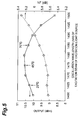
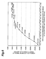
- Figure 6 is a graph illustrating the results of a test of output characteristic of an optical amplifier in the case where in particular the oscillation wavelength of the excitation beam is on the short wavelength side of 1480 nm; only the output power of the signal beam is plotted with respect to the oscillation wavelength of the excitation beam that is output from the semiconductor laser element.
- "[black diamond symbol]” indicates the output power (dBm) of the signal beam.
- the vertical axis indicates the amount of change ( ⁇ ) of the output power with respect to the output power of the signal beam when the oscillation wavelength of the excitation beam is 1480 nm.
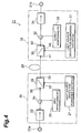
- the test was conducted under the following conditions with the optical amplifier shown in Figure 4.
- an optical amplifier by setting the oscillation wavelength of the excitation light source device on the short wavelength side of 1480 nm, which is the peak wavelength of the gain in an erbium-doped optical fiber, it is possible to make the amount of change of gain in the erbium-doped optical fiber satisfactorily small with respect to the amount of change of oscillation wavelength, and the wavelength dependence of the gain in an erbium-doped optical fiber can thereby be made satisfactorily small.
- the difference between the gain in the erbium-doped optical fiber when the temperature of the semiconductor laser element is high and when it is low can therefore be made satisfactorily small.
- the oscillation wavelength on the short wavelength side of 1480 nm which is the peak wavelength of gain in an erbium-doped optical fiber
- the NF can be made satisfactorily small and the wavelength dependence of the NF can be made small.
Landscapes
- Engineering & Computer Science (AREA)
- Physics & Mathematics (AREA)
- Chemical & Material Sciences (AREA)
- Electromagnetism (AREA)
- Optics & Photonics (AREA)
- Nanotechnology (AREA)
- Plasma & Fusion (AREA)
- Biophysics (AREA)
- Crystallography & Structural Chemistry (AREA)
- Life Sciences & Earth Sciences (AREA)
- Lasers (AREA)
- Semiconductor Lasers (AREA)
- Optical Communication System (AREA)
Abstract
Description
Claims (5)
- An optical amplifier comprising:wherein said semiconductor laser element comprises:an erbium-doped optical fiber;an excitation light source device having a semiconductor laser element that generates an excitation beam and a housing that accommodates said semiconductor laser element; andan optical multiplexer having a first input optically coupled with said excitation light source device, a second input for receiving a signal beam and an output for supplying said excitation beam and said signal beam to said erbium doped optical fiber;a first cladding layer that includes a chemical compound semiconductor of first conductivity type;a second cladding layer that includes a chemical compound semiconductor of second conductivity type; andan active layer provided between said first cladding layer and said second cladding layer;and wherein said semiconductor laser element has either of the following configurations (1)∼(3):(1) wherein said active layer contains a chemical compound semiconductor, and the oscillation wavelength of said semiconductor laser element at 20 °C is less than 1470 nm but not less than 1440 nm;(2) wherein said chemical compound semiconductor of the first conductivity type is InP semiconductor of the first conductivity type, said chemical compound semiconductor of the second conductivity type is TnP semiconductor of the second conductivity type, said active layer contains a chemical compound semiconductor, and the oscillation wavelength of said semiconductor laser element at 20 °C is less than 1470 nm; and(3) wherein said chemical compound semiconductor of the first conductivity type is InP semiconductor of the first conductivity type, said chemical compound semiconductor of the second conductivity type is InP semiconductor of the second conductivity type, said active layer has a multiple quantum well construction having a barrier layer and well layer including GaInAsP semiconductor, and the oscillation wavelength of said semiconductor laser element at 20 °C is less than 1470 nm.
- The optical amplifier according to claim 1 wherein said housing constituting said excitation light source device comprises a mounting member made of metal and said semiconductor laser element is arranged on said mounting member.
- The optical amplifier according to claim 1 or 2 wherein said housing constituting said excitation light source device comprises:a stem having a mounting portion on which said semiconductor laser element is mounted such that the optical axis of said semiconductor laser element faces a prescribed axial direction, a plurality of conductive pins having portions extending in said prescribed axial direction and an optical window through which passes light from said semiconductor laser element; anda cover member arranged on said stem so as to cover said semiconductor laser element.
- An optical amplifier comprising:an erbium-doped optical fiber;a first excitation light source device constituted by said excitation light source device of an optical amplifier according to claim 1;a first optical multiplexer having a first input optically coupled with said first excitation light source device, a second input for receiving a signal beam, and a first output for outputting said excitation beam and signal beam to said erbium-doped optical fiber;a second excitation light source device constituted by said excitation light source device of an optical amplifier according to claim 1; anda second optical multiplexer having a third input optically coupled with said second excitation light source device, a fourth input for receiving a signal beam and outputting an excitation beam to said erbium-doped optical fiber, and a second output for outputting said signal beam.
- The optical amplifier according to any of claims 1 to 4 wherein said excitation light source device is a non-temperature regulated light source device.
Applications Claiming Priority (2)
| Application Number | Priority Date | Filing Date | Title |
|---|---|---|---|
| JP2001361133A JP2003163396A (en) | 2001-11-27 | 2001-11-27 | Optical amplifier |
| JP2001361133 | 2001-11-27 |
Publications (2)
| Publication Number | Publication Date |
|---|---|
| EP1317037A2 true EP1317037A2 (en) | 2003-06-04 |
| EP1317037A3 EP1317037A3 (en) | 2005-07-06 |
Family
ID=19171841
Family Applications (1)
| Application Number | Title | Priority Date | Filing Date |
|---|---|---|---|
| EP02026453A Withdrawn EP1317037A3 (en) | 2001-11-27 | 2002-11-27 | Optical amplifier |
Country Status (3)
| Country | Link |
|---|---|
| EP (1) | EP1317037A3 (en) |
| JP (1) | JP2003163396A (en) |
| CN (1) | CN1422028A (en) |
Cited By (1)
| Publication number | Priority date | Publication date | Assignee | Title |
|---|---|---|---|---|
| EP2661794A4 (en) * | 2011-01-04 | 2014-07-16 | Ipg Photonics Corp | METHOD FOR STABILIZING THE OPTICAL OUTPUT POWER OF A FIBER LASER |
Families Citing this family (4)
| Publication number | Priority date | Publication date | Assignee | Title |
|---|---|---|---|---|
| JP2007288124A (en) * | 2006-03-22 | 2007-11-01 | Nippon Telegr & Teleph Corp <Ntt> | Optical fiber amplifier |
| JP2009059938A (en) * | 2007-08-31 | 2009-03-19 | Nippon Telegr & Teleph Corp <Ntt> | Optical fiber amplifier |
| JP2012080138A (en) * | 2012-01-24 | 2012-04-19 | Nippon Telegr & Teleph Corp <Ntt> | Optical fiber amplifier |
| JP6417199B2 (en) | 2014-12-08 | 2018-10-31 | 浜松ホトニクス株式会社 | Quantum cascade laser device |
Family Cites Families (5)
| Publication number | Priority date | Publication date | Assignee | Title |
|---|---|---|---|---|
| JPS59177986A (en) * | 1983-03-28 | 1984-10-08 | Matsushita Electric Ind Co Ltd | Manufacture of semiconductor laser |
| JPS59208886A (en) * | 1983-05-13 | 1984-11-27 | Hitachi Ltd | Light emitting semiconductor device |
| JPH03217065A (en) * | 1990-01-23 | 1991-09-24 | Toshiba Corp | Laser diode device |
| CA2369507A1 (en) * | 2000-02-03 | 2001-08-09 | The Furukawa Electric Co., Ltd. | Semiconductor laser module and pumping light source apparatus employing the same |
| WO2001064010A2 (en) * | 2000-03-03 | 2001-09-07 | Optical Technologies Italia S.P.A | Optical amplifier and optical transmission system |
-
2001
- 2001-11-27 JP JP2001361133A patent/JP2003163396A/en active Pending
-
2002
- 2002-11-27 EP EP02026453A patent/EP1317037A3/en not_active Withdrawn
- 2002-11-27 CN CN 02152744 patent/CN1422028A/en active Pending
Cited By (1)
| Publication number | Priority date | Publication date | Assignee | Title |
|---|---|---|---|---|
| EP2661794A4 (en) * | 2011-01-04 | 2014-07-16 | Ipg Photonics Corp | METHOD FOR STABILIZING THE OPTICAL OUTPUT POWER OF A FIBER LASER |
Also Published As
| Publication number | Publication date |
|---|---|
| JP2003163396A (en) | 2003-06-06 |
| EP1317037A3 (en) | 2005-07-06 |
| CN1422028A (en) | 2003-06-04 |
Similar Documents
| Publication | Publication Date | Title |
|---|---|---|
| US6950452B2 (en) | Semiconductor laser module and method for simultaneously reducing relative intensity noise (RIN) and stimulated brillouin scattering (SBS) | |
| JP4090402B2 (en) | Semiconductor optical amplifier and optical module using the same | |
| EP1246321B1 (en) | Cladding-pumped 3-level fiber laser/amplifier | |
| US20170187168A1 (en) | Optical semiconductor device, semiconductor laser module, and optical fiber amplifier | |
| US6288833B1 (en) | Optical device | |
| JPH041614A (en) | Optical amplifying device | |
| EP1085620A2 (en) | Lasers, optical amplifiers, and amplification methods | |
| JP2010232371A (en) | Semiconductor optical amplifier | |
| US20030091300A1 (en) | Semiconductor laser device, semiconductor laser module, Raman amplifier using the device or module, and method for forming a suitable current blocking layer | |
| US20030064537A1 (en) | Semiconductor laser device and method for effectively reducing facet reflectivity | |
| US6643308B2 (en) | Semiconductor laser device and method for suppressing injection current | |
| Juodawlkis et al. | Packaged 1.5-$\mu $ m Quantum-Well SOA With 0.8-W Output Power and 5.5-dB Noise Figure | |
| JP5505226B2 (en) | Semiconductor optical amplifier | |
| US6870667B2 (en) | Optical amplifier | |
| US6876680B2 (en) | Semiconductor laser device, semiconductor laser module, and optical fiber amplifier | |
| KR20040106676A (en) | Gain clamped semiconductor optical amplifier using raman gain mechanism | |
| US10511150B2 (en) | Wavelength-variable laser | |
| JP2003163396A (en) | Optical amplifier | |
| JP2002374037A (en) | Semiconductor laser module, fiber amplifier and optical communication system using the same | |
| JP6722829B2 (en) | Solid-state optical amplifier with active core and doped cladding in a single chip | |
| GB2408146A (en) | Semiconductor laser device, semiconductor laser module, and optical fiber amplifier | |
| EP1233490A2 (en) | Semiconductor laser module and fiber amplifier and optical communications system using the same | |
| JP3725498B2 (en) | Semiconductor laser device, semiconductor laser module, Raman amplifier using the same, and WDM communication system | |
| CN114792924A (en) | Doped fiber amplifier with straight-through pump laser | |
| JP4570319B2 (en) | Semiconductor laser device, semiconductor laser module, and semiconductor laser control method |
Legal Events
| Date | Code | Title | Description |
|---|---|---|---|
| PUAI | Public reference made under article 153(3) epc to a published international application that has entered the european phase |
Free format text: ORIGINAL CODE: 0009012 |
|
| AK | Designated contracting states |
Designated state(s): AT BE BG CH CY CZ DE DK EE ES FI FR GB GR IE IT LI LU MC NL PT SE SK TR |
|
| AX | Request for extension of the european patent |
Extension state: AL LT LV MK RO SI |
|
| PUAL | Search report despatched |
Free format text: ORIGINAL CODE: 0009013 |
|
| AK | Designated contracting states |
Kind code of ref document: A3 Designated state(s): AT BE BG CH CY CZ DE DK EE ES FI FR GB GR IE IT LI LU MC NL PT SE SK TR |
|
| AX | Request for extension of the european patent |
Extension state: AL LT LV MK RO SI |
|
| AKX | Designation fees paid | ||
| STAA | Information on the status of an ep patent application or granted ep patent |
Free format text: STATUS: THE APPLICATION IS DEEMED TO BE WITHDRAWN |
|
| 18D | Application deemed to be withdrawn |
Effective date: 20060110 |
|
| REG | Reference to a national code |
Ref country code: DE Ref legal event code: 8566 |