The present invention relates to a semiconductor laser device
and a semiconductor laser module using the device.
Conventionally, a semiconductor laser device as a light wave
oscillator which utilizes photon induced emission due to an optical
transition of electrons in a semiconductor crystal is widely known.
Such a semiconductor laser device generally includes a resonator and
oscillates a laser through light amplification by the resonator.
As the most basic structure of the resonator, the structure which
adopts a Fabry-Perot resonator composed of two parallel reflection
surfaces is known. Since the Fabry-Perot resonator can be easily
formed by cleaving the semiconductor crystal composing the
semiconductor laser device or polishing the semiconductor crystal into
a mirror finished surface, it is widely used when using a semiconductor
laser device as an ordinary light source.
However, in an optical communication system to be utilized for
data communication represented by Internet or the like, the
semiconductor laser device having the Fabry-Perot resonator is
insufficient. In the optical communication, it is necessary to increase
the intensity of a peak of a laser beam emitted from a semiconductor
laser device to be used as a signal light source or an excitation light
source in an emission wavelength and to reduce a half-width of the
peak. Particularly in a dense-wavelength division multiplexing
(DWDM) communication method which has been developed in recent
years, it is necessary to use a laser beam having a plurality of
wavelengths in a narrow wavelength range, and a half-width of peaks of
the respective laser beams should be very narrow. It is extremely
difficult to emit such a laser beam having a narrow half-value of a peak
from the semiconductor laser device using the Fabry-Perot resonator.
For this reason, there suggests a semiconductor laser module
which is provided additionally with a fiber grating in an optical fiber.
Fig. 13 shows a structure of such a semiconductor laser module. This
semiconductor laser module is composed of a structure such that a
semiconductor laser device 101 is optically coupled with an optical fiber
104 via a first lens 102 and a second lens 103. In order to carry out
laser oscillation, the resonator is composed of a reflection side end
surface 106 and a fiber grating 105 arranged in the optical fiber 104.
Since the fiber grating 105 has a sharp wavelength selection
characteristic, the structure shown in Fig. 13 makes a peak of an
oscillation laser beam sharp theoretically, and thus the peak intensity
increases.
Alternatively, there also suggest a semiconductor laser device in
which a diffraction grating is arranged in a vicinity of an active layer so
as to generate a DFB (distributed feed back) laser and a DBR
(distributed bragg reflector) laser which carry out single mode
oscillation, and a semiconductor laser device in which a diffraction
grating is arranged so as to generate a plurality of longitudinal
oscillation modes mainly having a constant wavelength. Such
semiconductor laser devices do not use a Fabry-Perrot resonator but
uses a resonator having an additional excellent wavelength selection
characteristic so as to obtain a sharp peak. This point is common to
the semiconductor laser module using a fiber grating.
However, it is known that the semiconductor laser devices which
include the resonator having the sharp wavelength selection
characteristic have a problem. The above-explained semiconductor
laser devices and laser module (hereinafter, referred to as
"semiconductor laser device and the like") normally have an emission
side end surface 107 in a laser emitting direction as shown in Fig. 13.
The emission side end surface 107 and the reflection side end surface
106 form the Fabry-Perot resonator. Therefore, an actual
semiconductor laser device and the like have a structure such that an
additionally provided resonator having a sharp wavelength selection
characteristic and the conventional Fabry-Perot resonator coexist. In
order to suppress amplification by the Fabry-Perot resonator, a
single-layer film made of alumina (Al2O3) or the like is laminated on the
emission side end surface 107 so that a reflectivity of a laser beam is
reduced on the emission side end surface 107. However, actually a
reflectivity of about 1 to 5 % remains and an influence of the
Fabry-Perot resonator cannot be eliminated completely.
On the contrary, a multi-layer film (hereinafter, referred to as
"equivalent single-layer film") which is optically equivalent to the
single-layer film is laminated on the emission side end surface so that a
reflectivity of a laser beam is made to be zero on the emission side end
surface. This technique is disclosed in Japanese Patent Application
Laid-Open No. 5-243689 (1993) (hereinafter, referred to as
"conventional art"). The reflectivity on the emission side end surface
becomes zero when the following equation is established,
nf = (ns no) 1/2
wherein nf is refractive index of the single-layer film, ns is an effective
refractive index of a semiconductor crystal composing the
semiconductor laser device, and n0 is a refractive index of an external
air contacting with the emission side end surface. When n0 is equal
with one since it is a refractive index of air, the refractive index of the
single-layer film is a square root of the effective refractive index of the
semiconductor crystal. For example, when the semiconductor crystal
composing the semiconductor laser device is made of InP, since ns
equals to 3.25 when an emission wavelength λ is 1480 nm, nf nearly
equals to 1.8. Since a material which satisfies the equation nf nearly
equals to 1.8 has a problem in a strength and the like when the
single-layer film is used as an actual transmission film, a plurality of
films having predetermined refractive index and thickness are laminated
so that an equivalent film of which entire refractive index becomes 1.8
is formed.
However, the conventional art has a problem. A wavelength of
a laser beam oscillated from the semiconductor laser device
occasionally deviates from a design value. When it is so, even when
the equivalent single-layer film is formed according to a calculated
value disclosed in the conventional art, the reflectivity zero cannot be
realized, and thus there is a problem that the reflectivity becomes large.
Since the refractive index is a function with respect to a wavelength of a
transmitting light, the wavelength of the laser beam deviates so that the
refractive index of plural materials forming the film also changes.
Therefore, the entire refractive index also changes naturally, and the
refractive index of the equivalent single-layer film obtains a value
different from the refractive index realizing entire reflection. When the
reflectivity due to this problem can be suppressed to an allowably low
value, there arises no problem.
However, the equivalent single-layer film of the conventional art
has a problem that a light of specified wavelength is not reflected but a
light of a wavelength other than the specified wavelength is reflected
greatly and thus the film functions as a cut filter as signified by the
inventors. In general, when scattering of a laser beam emitted from
the semiconductor laser device and scattering of film forming are taken
into consideration, it is necessary to allow an error of about ± 100 nm
with respect to the design value. Therefore, the above conventional
art has a problem in view of this point, and since the reflectivity of the
emission side end surface with respect to a light having deviated
wavelength becomes high, the Fabry-Perot resonator is formed.
In addition, the equivalent single-layer film of the conventional
art has a problem of controlling thicknesses of the plural films to be
laminated. In the conventional art, the equivalent single-layer film is
composed of a multi-layer film made of the respective films having
90.23 nm or 8.25 nm thickness; but when the film is grown by electron
beam vacuum evaporation, sputtering or the like, it is necessary to take
the possibility of lamination error of about ±5 % into consideration.
Therefore, the actually laminated equivalent single-layer film does not
occasionally have the reflectivity of zero due to the error of the
lamination thickness. For this reason, in order to suppress the forming
of the Fabry-Perot resonator effectively, it is necessary to previously
design a structure such that even when the error of the lamination
occurs, the reflectivity can be suppressed to a very low value.
In view of these problems, the film to be laminated on the
emission side end surface of the semiconductor laser device should
have a reflectivity of zero or an extremely low reflectivity with respect to
a wavelength which is deviated by a certain amount from the specified
wavelength, and even when the lamination error occurs in the film
growth, a fluctuation of the reflectivity should be small. However, a
study in view of this has not been particularly made until now.
It is an object of the present invention to provide a
semiconductor laser device and a semiconductor laser module in which
even when an oscillation wavelength and a thickness of films to be
laminated on an emission side end surface deviate, a reflectivity on the
emission side end surface becomes zero or obtains an extremely low
value and to provide method for providing a semiconductor laser device
having the extremely low reflectivity
According to one aspect of the present invention, there is
provided a semiconductor laser device and method for having a
reflection side end surface which reflects a laser beam to be oscillated
and an emission side end surface which emits the laser beam,
comprising a transmission film which includes a multi-layer film
laminated on the emission side end surface and having a low reflectivity
with respect to the laser beam to be emitted and having a structure of
plural films, wherein at least one-layer film of the multi-layer film is an
equivalent film which is optically equivalent to the one-layer film and
includes a plurality of films.
According to the above aspect, the multi-layer film structure
reduces the reflectivity with respect to the wavelength deviating from
the laser beam by a constant range and can suppress an influence of a
Fabry-Perot resonator as compared with when non-reflectivity is
realized by a single-layer film.
According to another aspect of the present invention, there is
provided a semiconductor laser module comprising, an
above-mentioned semiconductor device, a temperature control module
which controls a temperature of the semiconductor laser device, an
optical fiber which guides the laser beam emitted from the
semiconductor laser device to the outside, and an optically coupling
lens system which optically couples the semiconductor laser device with
the optical fiber.
According to the above aspect, the above-mentioned
semiconductor laser device is used, so that a laser beam, of which peak
intensity in the emission wavelength is large and half-width of the peak
is narrow, can be emitted.
The invention will be further described by way of example with reference to
the accompanying drawings, in which:-
Preferred embodiments of a semiconductor laser device and a
semiconductor laser module of the present invention will be explained
below with reference to the accompanying drawings. In the drawings,
the same or similar reference numerals are given to the same or similar
components. It is necessary to note that the drawings show typical
examples, and a relationship between a thickness and a width of a layer,
and a percentage of the thickness of the respective layers are different
from actual ones. Moreover, needless to say, the respective drawings
include parts that dimensional relationships and percentages are
different.
First embodiment
First, a semiconductor laser device according to a first
embodiment of the present invention will be explained. Fig. 1 is a side
sectional view which shows a structure of the semiconductor laser
device according to the first embodiment. The semiconductor laser
device of the first embodiment is constituted so that an n-InP cladding
layer 2, a GRIN-SCH-MQW active layer 3, a p-lnP cladding layer 4, a
p-lnGaAsP contact layer 5 and a p-side electrode 6 are laminated
sequentially on an n-InP substrate 1. Moreover, an n-side electrode 7
is arranged below the n-lnP substrate 1. Further, the semiconductor
laser device of the first embodiment is constituted so that a high
reflectivity film 8 is laminated on a reflection side end surface 16 (left
end surface in Fig. 1) and a transmission film 9 including a first film 10
and a second film 11 is laminated on an emission side end surface 15
(right end surface in Fig. 1). Further, the second film 11 is composed
of an equivalent film composed of three layers including a first sub-film
12, a second sub-film 13, and a third sub-film 14. Hereinafter, the film
having such a structure is referred to as an equivalent two-layer film.
The n-lnP cladding layer 2 and the p-lnP cladding layer 4 are
composed of substances having a larger band gap than the
GRIN-SCH-MQW active layer 3. This is because a carrier contributing
to laser oscillation is sealed in the GRIN-SCH-MQW active layer 3.
Moreover, the p-lnGaAsP contact layer 5 is provided so as to obtain
ohmic contact with the p-side electrode 6, and p-type impurity is doped
in a high-density manner. A wavelength of a laser beam emitted from
the semiconductor laser device in the first embodiment is 1480 nm.
The semiconductor laser device of the first embodiment has the
transmission film 9 including the first film 10 and the second film 11 on
the emission side end surface 15 as explained above. Further, the
second film 11 has the equivalent two-layer film structure composed of
the first sub-film 12, the second sub-film 13, and the third sub-film 14.
The transmission film 9 will be explained below.
In the semiconductor laser device of the first embodiment, a
resonator is not constituted by the emission side end surface 15 and
the reflection side end surface 16 unlike a semiconductor laser device
using the conventional Fabry-Perot resonator. In the semiconductor
laser device of the first embodiment, the resonator is composed of the
high reflectivity film 8 laminated on the reflection side end surface 16
and an external diffraction grating such as a fiber grating exemplified in
Fig. 13. Therefore, the high reflectivity film 8 is composed of a
substance which realizes a reflectivity of a certain degree, whereas the
transmission film 9 laminated on the emission side end surface 15
should have a reflectivity which is low as in order to prevent the
Fabry-Perot resonator from being formed, and more preferably it is
necessary to set the reflectivity of an oscillation laser beam on the
emission side end surface 15 to 0. The reflectivity is a ratio between
input optical strength and reflecting optical strength when light having
specific wavelength is input from outside to the emission side end
surface 15. The reflectivity of the emission side end surface 15 can be
determined by measuring the strength of the input and reflected light.
However, since the semiconductor laser devices are very small,
generally the reflectivity is calculated by examining the composition of
the semiconductor laser device. Precisely, a Scanning Electron
Microscope (SEM) is used to measure the thickness of a thin film
structure, which has a plurality of thin films, that is laminated on the
emission side end surface 15. Moreover, an Auger Electron
Spectroscope (AES) is used to calculate the composition of each thin
film in the thin film structure. The reflectivity of the emission side end
surface 15 is precisely calculated using the calculated composition in a
spectroscopic ellipsometry. The reflectivity mentioned below is either
calculated using the method described above or really measured.
In addition, in the actual semiconductor laser device, the
wavelength of the laser beam to be emitted fluctuates due to a level of
an electric current to be injected into the GRIN-SCH-MQW active layer
3 or a temperature of the GRIN-SCH-MQW active layer 3. Moreover,
the emission wavelength of a produced semiconductor laser device
occasionally obtains a value different from a value at the stage of the
design. Therefore, it is necessary to constitute the transmission film 9
so that it allows a light to transmit not only in a specified wavelength but
the reflectivity of a light deviating by a constant wavelength range from
a the specified wavelength on the emission side end surface 15
becomes low or zero. Specifically, it is necessary to constitute the
transmission film 9 so that the Fabry-Perot resonator is not formed for a
light which deviates by about ± 100 nm with respect to the specified
wavelength.
Further, it is necessary to heighten tolerance of an error in the
actual formation of the film. In the actual film growth, since there
occurs an error on the film thickness of about ± 5 %, it is necessary that
even when the error occurs, the reflectivity on the emission side end
surface 15 obtains a low value which can be allowed.
Based on these points, it is necessary to design the structure of
the first film 10 and the second film 11 composing the transmission film
9, and the structure of the first sub-film 12, the second sub-film 13, and
the third sub-film 14 composing the second film 11. In the following
explanation, a refractive index of the first film 10 is n1 and its thickness
is d1, and the second film 11 has a refractive index n2 and a thickness
d2. Similarly, the first sub-film 12 has a refractive index n2a and a
thickness d2a, the second sub-film 13 has a refractive index n2b and a
thickness d2b, and the third sub-film 14 has a refractive index n2c and a
thickness d2c. In the following explanation, these refractive indexes
are values with respect to a wavelength of a laser beam emitted from
the semiconductor laser device of the first embodiment.
First, a relationship between n1, d1, n2, d2 and a reflectivity of an
oscillation laser beam on the emission side end surface 15 will be
explained. An oscillation wavelength of the laser beam is λ, and a
refractive index of the GRIN-SCH-MQW active layer 3 is ns. Moreover,
a refractive index n0 of an external air contacting with the first film 10 is
n0. The following equations realize the reflectivity zero with respect to
the specified wavelength λ in a general two-layer film.
tan2δ1 = n1 2(ns-n0)(n2 2-n0ns)/{(n1 2ns-n2 2n0) (n0ns-n1 2)}
tan2δ2 = n2 2(ns-n0)(n0ns-n1 2)/{(n1 2ns-n2 2n0) (n2 2-n0ns)}
δj = 2πnjdj / λ (j = 1,2). In the equations (2) and (3), n0 is the
refractive index of external air (with air, 1.0), and ns is a constant which
is determined by a material of the semiconductor laser device.
Therefore, the equations (2) and (3) are equations in which n1, d1, n2
and d2 are variables, and two variables of the four variables are
determined, so that the structures of the first film 10 and the second
film 11 can be determined from the equations (2) and (3).
In general, the refractive index n
s of the GRIN-SCH-MQW active
layer 3 obtains a value of 3 to 4, and accordingly the refractive indexes
n
1 and n
2 of the first film 10 and the second film 11 can be obtained
from the equations (2) and (3) as the following table.
| Refractive index ns of active layer | Refractive index n1 of the first film | Refractive index n2 of the second film |
| 3 | 1.1 | 1.8∼1.9 |
| ∼ |
| 1.7 | 1.8∼2.9 |
| 3.25 | 1.1 | 1.9 |
| ∼ |
| 1.8 | 1.9∼3.2 |
| 3.5 | 1.1 | 1.9∼2.0 |
| ∼ |
| 1.8 | 1.9∼3.3 |
| 3.75 | 1.1 | 2.0∼2.1 |
| ∼ |
| 1.9 | 2.0∼3.6 |
| 4 | 1.1 | 2.1 |
| ∼ |
| 1.9 | 2.1∼3.7 |
Therefore, when the refractive indexes ns and n1 are determined,
the refractive index n2 of the second film 11 is also determined, and the
film structures of the first sub-film 12, the second sub-film 13, and the
third sub-film 14 can be determined so that the refractive indexes
having such values are realized.
Next, a method of determining the structures of the first sub-film
12, the second sub-film 13, and the third sub-film 14 composing the
second film 11 will be explained. In general, a film having constant
refractive index and thickness can be expressed by a characteristic
matrix M which is a two-dimensional square matrix. When an element
of the characteristic matrix Mk is mij (1≤i, j≤2), generally a film having
refractive index nk and thickness dk can be expressed by the following
equations,
m11 = m22 = cosk
m12 = ink -1sink
m21 = inksink
where is equal to 2πnkdk/λ, and i is an imaginary unit. The first
sub-film 12, the second sub-film 13, and the third sub-film 14 also can
be defined in the similar manner, and thus a characteristic matrix of the
second film 11 is M2, a characteristic matrix of the first sub-film 12 is
M2a, a characteristic matrix of the second sub-film 13 is M2b and a
characteristic matrix of the third sub-film 14 is M2c. A relationship
between M2, M2a, M2b and M2c is represented by the following equation,
M2 = M2a*M2b*M2c
Since the equation (7) is a relational expression of the two-dimensional
square matrix, equations are established for the respective elements of
the matrix, and actually four equations are established. When the
refractive index n1 of the first film 10 and the refractive index n2 of the
second film 11 are determined in the equations (2) and (3), four
equations exist for six variables n2a, d2a, n2b, d2b, n2c and d2c.
Therefore, when arbitrary two of these variables are determined, the
rest variables are also obtained by the equation (7). Accordingly, the
structures of the first sub-film 12, the second sub-film 13, and the third
sub-film 14 are determined.
In the first embodiment, the first sub-film 12 and the third
sub-film 14 are formed by the same material and are designed so as to
have the equal film thickness. This is because a multi-layer film
having a symmetrical structure with respect to a center surface is
equivalent to a single-layer film according to A. Thelen, "Physics of Thin
Films", Vol. 5, Academic Press, New York (1969). Moreover, this is
because the same material is used, so that the producing steps can be
simplified. Therefore, in the first embodiment, n2a is equal to n2c and
d2a is equal to d2c, and the variables in the equation (7) are reduced to
four so that all the values of the variables can be obtained.
According to the above explanation, the refractive index n1 of
the first film 10 and the refractive index n2 of the second film 11 are
determined and the equations (2) to (7) are calculated, so that the
structures of the first sub-film 12, the second sub-film 13, and the third
sub-film 14, composing the second film 11, and the structure of the first
film 10 can be determined. Therefore, the structure of the
transmission film 9 composed of the first film 10 and the second film 11
is determined.
Next, a method of determining the refractive index n1 of the first
film 10 and the refractive index n2 of the second film 11 will be
explained. First, a substance composing the first film 10 is determined.
The first film 10 is not an equivalent film as shown in Fig. 1 and is
composed of one kind of a material, and thus a composing material is
determined so that the refractive index n1 is determined.
A specific material composing the first film 10 is Al2O3 in the first
embodiment. Al2O3 has been conventionally known as a material of a
low reflectivity film, and its characteristic and film growth have been
studied in various manners. Therefore, it is confirmed that Al2O3 easily
grows on an end surface of the semiconductor laser device and it is
stable during the long-time use of the semiconductor laser device.
When the first film 10 is composed of Al2O3, the refractive index n1
becomes 1.620 with respect to a light having a wavelength λ of 1480
nm.
In addition, a composing material of the second film 11 is also
previously determined. Since the first sub-film 12, and the third
sub-film 14 have the same refractive index as explained above, they are
composed of the same material. In the first embodiment, the first
sub-film 12, and the third sub-film 14 are made of Al2O3, and the
second sub-film 13 is made of amorphous silicon (hereinafter, referred
to as "α-Si"). Al2O3 is used because it grows easily and is stable
during the long-time use and also as the first sub-film 12 and the first
film 10 are adjacent to each other, thus the same material is used for
these two films so that the first sub-film 12 and the first film 10 can be
grown sequentially. Moreover, α-Si is used for the second sub-film 13
because, similarly to Al2O3, it is a known material and makes film
growth easy on the end surface and is stable during the long-time use.
As understood from the equation (7), the refractive index n2 of
the second film 11 cannot be determined only by determining the
composing materials of the first sub-film 12, the second sub-film 13 and
the third sub-film 14. Whereas in the first embodiment, since the
refractive index n1 has been already determined, when the refractive
index n2 is determined, all parameters composing the transmission film
9 are determined by the equations (2) to (7).
According to the above explanation, the refractive index n1 is
already determined. Therefore, in order to obtain the transmission film
9 which have a large tolerance of the lamination error and can realize a
very low reflectivity in a wavelength which deviates from the specified
wavelength, the refractive index n2 is set to various values, and
characteristic of the transmission film 9 are studied, and a range of the
refractive index n2 is determined, so that the structure of the
transmission film 9 is determined.
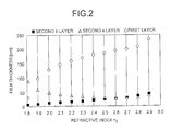
Fig. 2 is a graph which shows the film thickness d1, d2a and d2b
of the respective layers with respect to a fluctuation of the refractive
index n2. Since the thickness d2c of the third sub-film 14 has the same
value as the thickness d2a, it is not shown on the graph. The range of
the refractive index n2 is 1.8 to 3.0 in Fig. 2 because when the
refractive index is 1.8, this is the same as a refractive index when the
single-layer film of the conventional art is represented by a transmission
film, and thus the first layer 10 is not necessary and an advantage of
the multi-layer film is eliminated. Moreover, the reason that the upper
limit is 3 is as follows. The main material of the semiconductor laser
device of the first embodiment is InP, and the refractive index ns is 3.25.
Therefore, when the refractive index n2 exceeds 3, a difference with the
refractive index of the semiconductor laser device is substantially
eliminated, and thus the provision of the second film 11 becomes
meaningless.
According to Fig. 2, as the refractive index n2 becomes larger,
the film thickness of the first film 10 and the second sub-film 13
increase, and the film thickness of the first sub-film 12 becomes
minimum in a vicinity of the refractive index n2 is equal to 2.5. These
values are obtained by calculating the equations (2) to (7) where n2 is a
variable.
Figs. 3A and 3B are graphs which show a tendency of a change
of the reflectivity on the emission side end surface 15 with respect to
the lamination error in the structure of the transmission film 9
determined in Fig. 2. Fig. 3A shows as to how much a laser beam is
reflected on the emission side end surface 15 when the thickness of the
first film 10, the first sub-film 12, and the third sub-film 14 made of
Al2O3 deviate from the design values by ± 10 %. Moreover, Fig. 3B
shows a reflectivity on the emission side end surface 15 when the film
thickness of α-Si composing the second sub-film 13 deviates from the
design value by ± 10 %. In the actual film growth, an error can be
normally suppressed to ± 5 % or less, but in Figs. 3A and 3B, in order
to clearly show the tendency of the change of the reflectivity with
respect to the lamination error, the lamination error is assumed to be
large.
As shown in Fig. 3A, as for Al2O3, when the refractive index n2
of the second film 11 is previously designed to be larger, the reflectivity
can be suppressed low even when the lamination error occurs.
Particularly, the reflectivity can be suppressed remarkably when the
lamination error is + 10 %. On the contrary, as for the lamination error
of α-Si, as shown in Fig. 3B, when the refractive index n2 is designed to
be large, the reflectivity on the emission side end surface 15 becomes
large.
Therefore, Figs. 3A and 3B show opposite results respectively,
but since the reflectivity due to the lamination error of the α-Si is
maximally 0.05 %, that is very low, an actual problem does not arise.
For this reason, in order to suppress the reflectivity with respect to the
lamination error of Al2O3, the refractive index n2 of the second film 11 is
desirably about 2.4 to 3.0. With such a limitation, when the lamination
error in the actual film growth is within ± 5 %, the reflectivity due to the
lamination error can be suppressed to about 0.35 % maximally. In the
first embodiment, as a specific example to study a characteristic in this
range, the structure where n2 is equal to 2.5 and the structure where n2
is equal to 2.92 are selected. When n2 is equal to 2.5, according to the
equations (2) to (7), d1 is equal to 187.3 nm, d2a and d2c are equal to
29.7 nm, and d2b is equal to 23.9 nm. Moreover, when n2 is equal to
2.92; similarly according to the equations (2) to (7), d1 is equal to 216.0
nm, d2a and d2c are equal to 50.2 nm and d2b is equal to 46.8 nm.
Fig. 4A shows a change of the reflectivity with respect to the
emission wavelength λ in the transmission film where n2 is equal to 2.92.
In Fig. 4A, a curved line I1 shows a change of the reflectivity of the
transmission film 9 having the equivalent two-layer film structure in the
first embodiment, and a curved line I2 shows a change of the reflectivity
when the second film 11 is composed of a single film. It is not realistic
that the second film 11 is composed of a single film in view of selection
of a material, and the curved line I2 is only a logical value which is
shown for comparison with the curved line I1.
As for the curved line I1 relating to the transmission film 9 of the
first embodiment, the reflectivity becomes remarkably large in a
wavelength area where the wavelength λ is 1300 nm or less as
compared with the curved line I2 relating to the single film. However, in
the first embodiment, the reflectivity may be zero or very low in the
range of 1380 nm ≤ λ ≤ 1580 nm, there arises no problem. When the
wavelength λ is in the range of 1380 nm ≤ λ ≤ 1580 nm, the curved line
I1 relating to the transmission film 9 substantially matches with the
curved line I2 relating to the single film. For this reason, when the
refractive index n2 of the second film 11 is 2.92, the second film 11 is
composed of an equivalent film, so that the performance which is
substantially equal with when using the single film can be secured.
Similarly, Fig. 4B shows a change of the reflectivity with respect
to the emission wavelength λ in the transmission film where n2 is equal
to 2.5. In Fig. 4B, a curved line I3 shows a change of the reflectivity of
the transmission film 9 in the first embodiment, and a curved line I4
shows a change of the reflectivity when the second film 11 is composed
of a single film.
Fig. 4B shows a graph in which when n2 is equal to 2.5, the
reflectivity can be suppressed lower in any wavelength ranges when the
second film 11 is composed using the equivalent two-layer film in the
first embodiment as compared with when the second film 11 is
composed of the single film. Moreover, overlapping is seen in Fig. 4B,
but even when the emission wavelength λ is in the range of 1380 nm ≤
λ ≤ 1580 nm, the equivalent two-layer film of the first embodiment has
an excellent characteristic as compared with the two-layer film
composed of the single film.
As shown in Figs. 4A and 4B, when compared with the two-layer
film in which the second film 11 is composed of the single film, the
equivalent two-layer film of the first embodiment can realize the
equivalent or lower reflectivity in a wavelength range which deviates
from the design wavelength.
Next, the reflectivity of the conventional equivalent single-layer
film structure in which the single film is replaced by a multi-layer film is
compared with the reflectivity of the transmission film 9 which is the
equivalent two-layer film of the first embodiment. In Fig. 5A, a curved
line I5 shows the reflectivity of the equivalent single-layer film of the
conventional art, and a curved line I6 shows the reflectivity of the
equivalent two-layer film of the first embodiment in which n2 is equal to
2.92. Moreover, a curved line I7 shows the reflectivity of the equivalent
two-layer film in which n2 is equal to 2.5. As compared with the
conventional art, the transmission film 9 of the first embodiment has a
lower reflectivity than the conventional art in the wavelength area where
the emission wavelength λ is 1350 nm or more according to a change of
the emission wavelength λ. When the emission wavelength λ is 1350
nm or less, the reflectivity of the equivalent two-layer film in which n2 is
equal to 2.92 is high, but it is not particularly a problem in view of the
oscillation wavelength range of the semiconductor laser device.
Fig. 5B shows the enlarged range of 1380 nm ≤ λ ≤ 1580 nm on
the graph of Fig. 5A. According to this, it is found that in the
wavelength range of 1380 nm ≤ λ ≤ 1580 nm which is an assumed
emission wavelength of the semiconductor laser device of the first
embodiment, the transmission film 9 of the first embodiment realizes
the lower reflectivity than the conventional art. Particularly when n2 is
equal to 2.5, the maximum value of the reflectivity can be suppressed to
about 0.25 %. When n2 is equal to 2.92, the reflectivity is
approximately the same as that of the equivalent single-layer film of the
conventional art in the range of λ ≤ 1480 nm, but in the range of 1480
nm ≤ λ, the reflectivity can be suppressed lower.
As shown in Fig. 5B, the reflectivity of the transmission film 9 of
the first embodiment can be suppressed lower than the equivalent
single-layer film of the conventional art. Furthermore, when n2 is equal
to 2.92, it has the equivalent or excellent characteristic to the
equivalent single-layer film of the conventional art, and when n2 is equal
to 2.5, it has more excellent characteristic. For this reason, at least
when the refractive index ns of the semiconductor laser device is 3.25,
the refractive index n2 of the second film 11 is set within the range of
2.5 to 2.92, so that the transmission film which is more excellent than
the conventional art can be provided. As it is clear from Fig. 5B, as
the refractive index n2 becomes smaller, the more excellent
characteristic is displayed, and thus when the lamination error can be
suppressed low at the time of the film growth, it is desirable that the
refractive index n2 is 2.5 or less.
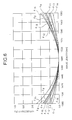
How the reflectivity changes with change in a refractive index of
the second film 11 will be explained here. Fig. 6 is a graph showing a
change in reflectivity when the refractive index n2 of the second layer 11
is changed from 1.9 to 2.8, in the wavelength range of 1380 nm ≤ λ ≤
1580 nm. Precisely, a curved line I8 shows a change in the reflectivity
when n2 is equal to 1.9 and curved lines I9, I10, I11, I12, I13, I14 show
changes in reflectivity when n2 is equal to 2, 2.1, 2.3, 2.5, 2.7, 2.8
respectively. A curved line I15 is provided for comparison. The line I15
shows a change in reflectivity of the equivalent single-layer film
explained in description of the conventional art,
It is clear from Fig. 6 that the semiconductor laser device having
equivalent two-layer film structure as in the first embodiment shows
lower reflectivity, for all the refractive indexes at which the reflectivity is
calculated, compared to the conventional equivalent single-layer film.
From this result, using equivalent multi-layer film like the equivalent
two-layer film instead of equivalent single-layer film is more effective for
making a film structure that lowers reflectivity for the specific
wavelength range. Specifically, when the equivalent two-layer film is
used, reflectivity can be suppressed below 0.4 % in a wide wavelength
range of 1380 nm ≤ λ ≤ 1580 nm, which is the wavelength range where
the difference between assumed emission-wavelength is below 100nm
regardless of refractive index n2. More favorably, when the value of
refractive index n2 is equal to or greater than 2.7 (curves I13, I14), the
reflectivity can be kept below 0.2 % in a wavelength range of 1380 nm ≤
λ ≤ 1580 nm.
The semiconductor laser device shown in Fig. 1 has the
resonator which is composed of the reflection side end surface 16 and
the external diffraction grating, not shown, but the resonator can have
another structure. For example as shown in Fig. 8, the resonator may
be DFB laser in which a p-lnP spacer layer 20 is provided between the
GRIN-SCH-MQW active layer 3 and the p-lnP cladding layer 4, and a
diffraction grating 21 is arranged inside the p-lnP spacer layer 20.
When it is made so, since the resonator is composed of the diffraction
grating 21 and the high reflectivity film 8, it has an advantage that a
diffraction grating should not be arranged on the outside. The spacer
layer is arranged below the GRIN-SCH-MQW active layer 3, and the
diffraction grating may be provided inside the spacer layer, and an
electrically conductive type of the spacer layer then may be desirably n
type.
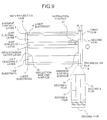
In addition, as shown in Fig. 9, a p-lnP spacer layer 22 is
arranged between the GRIN-SCH-MQW active layer 3 and the p-lnP
cladding layer 4, and a diffraction grating 23 may be arranged partially
inside it. A length of the semiconductor laser device in the laser beam
emitting direction, a period of the diffraction grating, a value of a
coupling coefficient and the like are devised, so that a laser beam
having a plurality of oscillation longitudinal modes with respect to a
certain constant center wavelength can be emitted. The transmission
film 9 composed of the equivalent two-layer film of the first embodiment
is arranged on the emission side end surface 15, so that the half-width
of the peak of the respective oscillation longitudinal modes are
expected to be capable of being narrowed and a wavelength distance
between the oscillation longitudinal modes is expected to be capable of
being narrowed.
Actually, an emission wavelength spectrum of a laser beam is
measured in the semiconductor laser device having the structure shown
in Fig. 9 to which the transmission film 9 of the first embodiment is
applied and in a semiconductor laser device to which the conventional
transmission film (reflectivity, 1.5 %) is applied. The semiconductor
laser devices which are constituted so that the diffraction grating is
provided inside and the resonator is composed of the reflection film
formed on the reflection side end surface and the diffraction grating is
used. When the values of the injection electric current I are 200 mA,
500 mA and 900 mA, the emission wavelength spectrum was measured.
The respective semiconductor laser devices were produced under the
same condition except the transmission films.
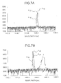
Fig. 7A shows the spectrum of the semiconductor laser device to
which the transmission film 9 of this embodiment is applied, and Fig. 7B
shows the spectrum of the semiconductor laser device to which the
transmission film having reflectivity of about 1.5 % is applied. In Fig.
7A, a curved line I16 shows a spectrum when the injection electric
current I is 200 mA, a curved line I17 shows a spectrum when I is 500
mA, and a curved line I18 shows a spectrum when I is 900 mA.
Moreover, in Fig. 7B, a curved line I19 shows a spectrum when I is 200
mA, a curved line I20 shows a spectrum when I is 500 mA, and a curved
line I21 shows a spectrum when I is 900 mA.
As for the whole tendency, it is found that in the semiconductor
laser device to which the transmission film 9 of the first embodiment is
applied, the peak intensity is strong and the half-width of the peak is
narrow. The curved line I18 and the curved line I21 of I = 900 mA which
are remarkably different from each other will be compared.
The half-width of the peak waveform on the curved line I21 is
wide and forms a deformed waveform. Further, another broad peak
exists in the vicinity of 1480.2 nm. On the contrary, the curved line I18
has a peak of narrow half-width, and a peak in another wavelength does
not exist.
As a result, as compared with the semiconductor laser device
using the conventional transmission film, the semiconductor laser
device to which the equivalent two-layer film of the first embodiment is
applied has high light emission efficiency and has the narrow half-width
of the peak in the oscillation wavelength. For this reason, according to
the first embodiment, it is found that the semiconductor laser device,
which has excellent characteristic as a signal light source or an
excitation light source in optical communication, can be provided.
The transmission film composed of the equivalent two-layer film
of the first embodiment can be effectively applied also to DBR laser in
which the diffraction grating, not shown, is arranged inside the
semiconductor laser device and the p-side electrode is not arranged
above the diffraction grating. Namely, it is effective, for all
semiconductor laser devices which do not use the Fabry-Perot
resonator, to laminate the transmission film composed of the equivalent
two-layer film of the first embodiment on the emission side end surface.
As explained above, in the semiconductor laser device of the
first embodiment, the equivalent two-layer film is used for the
transmission film 9. By utilizing the equivalent film structure, a
substance having an arbitrary refractive index in the substances having
the refractive index in the predetermined range can be used as a
material of the film in order to realize the non-reflectivity two-layer film.
As a result, for example, a widely used substance of which
characteristic is clear such that it can withstand the long-time use, can
be used. Therefore, as compared with when a special single
substance is used for the second film 11 in order to realize a desirable
refractive index, the durability against the long-time use of the
semiconductor laser device or the like can be heightened. Moreover,
as compared with when using the special material, the production cost
can be made to be low, and the production can be facilitated.
In addition, the use of the equivalent two-layer film can suppress
the reflectivity on the emission side end surface 15 of the
semiconductor laser device in a constant wavelength range to a very
low value of zero or about 0.25 % or less. Therefore, this can prevent
the reflection side end surface 16 and the emission side end surface 15
from forming the Fabry-Perot resonator. As a result, the half-width of
the laser oscillation wavelength peak can be narrowed and the peak
intensity can be increased. Further, these advantages are greater than
those of the equivalent single-layer film, and the same effect which is
not less than equivalent to the two-layer film not using an equivalent
film is achieved.
Further, a change of the refractive index of the equivalent
two-layer film with respect to an error of a thickness of a film to be
laminated is small, and thus when an error occurs, the reflectivity can
be suppress maximally to 0.3 %, namely, a very low value. As a result,
in the actual production of the semiconductor laser device, the error at
the time of the lamination of the films can be allowed to a certain
degree, and the yield can be improved.
In addition, in the first embodiment, the transmission film 9 as
the equivalent two-layer film is composed of Al2O3 and α-Si. These
substances are well known as a film material, and an apparatus which
grows a film, a growing technique and the like have been already
established. Therefore, use of these substances enables the film
growth to be carried out easily by utilizing the conventional production
technique.
In the first embodiment, the transmission film 9 has the structure
that the first film 10 is composed of the single-layer film and the second
film 11 is composed of the equivalent film, but it is not necessarily
limited to this. More specifically, the second film 11 may be composed
of the single-film and the first film 10 may be composed of the
equivalent film.
Further, the transmission film 9 does not have the two-layer film
structure but have a multi-layer film structure composed of three or
more-layer films, arbitrary one or plural film(s) of the three films may be
replaced by an equivalent film. The method of setting the reflectivity in
a specified wavelength to zero by the multi-layer film structure is known,
and it is known that the multi-layer film structure can realize a low
reflectivity in a wide wavelength range as compared with the
single-layer film structure. Therefore, when it is combined with the
equivalent film structure, it is expected to realize a transmission film
having low reflectivity characteristic equivalent to or more excellent
than that of the multi-layer film structure of which respective layers are
composed of a single film as shown similarly in the first embodiment.
Further in the first embodiment, the material of the transmission
film 9 is Al2O3 and α-Si, but the material is not naturally limited to these.
Since the equivalent multi-layer film structure including the equivalent
two-layer film can realize a film having a desirable refractive index by a
substance having an arbitrary refractive index, the transmission film 9
can be naturally composed of a substance other than Al2O3 and the
like.
In addition, the emission wavelength λ of the semiconductor
laser device is 1480 nm in the first embodiment, but the emission
wavelength is not limited to this, and the semiconductor laser device is
not limited to the structure mainly having InP. The emission
wavelength λ is 1480 nm in this embodiment because the device is
simply assumed to be used as an excitation light source in the erbium
doped optical fiber amplifier (EDFA). Even when a semiconductor
laser device of another wavelength is produced by mainly using another
semiconductor, the structure of the transmission film can be determined
by the above-mentioned method.
The inventors of the present invention tried to optimize the film
thickness and the like of the transmission film 9 in the semiconductor
laser device that emits a laser beam with a wavelength of 980nm which
is used as excitation light of EDFA. More precisely, the inventors
prepared a semiconductor laser device having the transmission film 9
shown in Fig. 1 and that emits a light of wavelength of 980 nm. The
first film 10 is formed with Al2O3, having refractive index n1 of 1.62, and
a film thickness of 67.8 nm. The second film 11 has a refractive index
n2 of 2.00, with a film thickness of 83.6. The second film 11 employs
the equivalent film structure.
The second film 11 is comprised of a first sub-film 12, a second
sub-film 13, a third sub-film 14. The first sub-film 12 is formed of Al2O3
and has a refractive index n2a of 1.62. The second sub-film 13 is
formed of TiO2 and has a refractive index n2b of 2.25. The third
sub-film 14 is formed of Al2O3 and has a refractive index n2c of 1.62.
The thickness of the first sub-film 12, d2a, is 22.8 nm, the thicknesses of
the second film, d2b, is 41.3 nm, and the thicknesses of the third film,
d2c, is 22.8 nm. The reflectivity obtained due to such a structure is
shown as a curve I22 in Fig. 10. As it is apparent from the curve I22 in
Fig. 10, the reflectivity becomes 0 % at the wavelength of 980 nm and it
is low even in the other range.
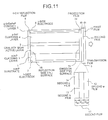
When the transmission film 9 is mounted on the semiconductor
laser device which emits a light of wavelength of 980 nm, it is favorable
to provide a protection film 24 between the emission side end surface
15 and the second film 11 as shown in Fig. 11. The protection film 24
is provided to protect the emission side end surface 15. Precisely, the
protection film 24 suppresses oxidization of the emission side end
surface 15 from aging, and generation of catastrophic optical damage
(COD) of the emission side end surface 15.
Reflectivity curve when a protection film is simply provided in
the structure of the transmission film 9 is shown as a curve I23 in Fig. 10.
The protection film is made of the semiconductor material InGaP. This
protection film has a refractive index of 3.21 and thickness of 100 nm.
The curve I23 shows that the 0 % reflectivity is shifted to short
wavelength side from wavelength of 980 nm, and desired reflectivity
cannot be gained in the range of 900 nm to 1100 nm.
On the contrary, when new film is provided to the emission side
end surface 15, it is possible to optimize each thickness of the first film
10, the first sub-film 12, the second sub-film 13, and the third sub-film
14 by the simplex method or the anneal method. The inventors of the
present invention optimized the films using the simplex method and
gained the result of the thickness of the first film d1 as 97.3 nm, the
thickness of the first sub-film d2a as 17.1 nm, the thickness of the
second sub-film d2b as 34.4 nm, and the thickness of the third sub-film
d2c as 17.1 nm. A curve I24 in Fig. 10 shows wavelength change of the
reflectivity gained from the result above. It is apparent from the curve
I24 that even if the protection film is provided, reflectivity becomes 0 %
at 980 nm and also kept low in the wavelength range of 900 nm to 1100
nm. Moreover, the reflectivity of the emission side end surface 15 in
optimized semiconductor laser device with the protecting film is kept
low compared to the semiconductor laser device without the protecting
film in the entire wavelength range of 900 nm to 1100 nm. Therefore,
when the protection film is formed by InGaP, there is an advantage in
terms of reflectivity suppression as well as preventing oxidization and
generation of COD in the emission side end surface 15.
Second embodiment
A second embodiment of the present invention will be explained.
In the second embodiment, the semiconductor laser device shown in
the first embodiment is used in a laser module.
Fig. 12 is a side sectional view which shows a structure of the
semiconductor laser module according to the second embodiment of the
present invention. The semiconductor laser module of the second
embodiment has a semiconductor laser device 31 corresponding to the
semiconductor laser device shown in the first embodiment. The
semiconductor laser device 31 has a junction-down structure that the
p-side electrode is jointed to a heat sink 38. A temperature control
module 40 as a temperature control unit is arranged on an internal
bottom surface of a package 41 which is formed as a housing of the
semiconductor laser module by ceramic or the like. A base 37 is
arranged on the temperature control module 40, and a heat sink 38 is
arranged on the base 37. An electric current, not shown, is supplied to
the temperature control module 40, cooling or heating is carried out
according to polarity of the electric current. However, in order to
prevent the oscillation wavelength from deviating due to a rise of the
temperature of the semiconductor laser device 31, the temperature
control module 40 functions mainly as a cooler. When a laser beam
has a longer wavelength than a desired wavelength, the temperature
control module 40 cools and controls to a low temperature, and when a
laser beam has a shorter waveform than the desired wavelength, the
temperature control module 40 heats and controls to a high temperature.
Specifically, this temperature control is carried out based on a detected
value of a thermistor 39 which is arranged on the heat sink 38 in the
vicinity of the semiconductor laser device 31, and a control unit, not
shown, normally controls the temperature control module 40 so that the
temperature of the heat sink 38 is kept constant. Moreover, the control
unit, not shown, controls the temperature control module 40 so that the
temperature of the heat sink 38 drops as a driving current of the
semiconductor laser device 31 is raised. When such a temperature
control is carried out, output stability of the semiconductor laser device
31 can be improved, and the yield is also improved effectively. It is
desirable that the heat sink 38 is formed by a substance having high
thermal conductivity such as diamond. This is because when the heat
sink 38 is formed by diamond, heat generation at the time of applying a
high electric current is suppressed.
The heat sink 38 on which the semiconductor laser device 31
and the thermistor 39 are arranged, a first lens 32 and an electric
current monitor 36 are arranged on the base 37. A laser beam emitted
from the semiconductor laser device 31 is guided via the first lens 32,
an isolator 33 and a second lens 34 onto an optical fiber 35. The
second lens 34 is on an optical axis of the laser beam and is provided
on the package 41 and is optically coupled with the optical fiber 35 to
be externally connected. The electric current monitor 36 detects a
light leaked from a high reflectivity film side of the semiconductor laser
device 31.
In this semiconductor laser module, the isolator 33 intervenes
between the semiconductor laser device 31 and the optical fiber 35 so
that a reflected return light from other optical parts do not return into the
resonator. When the semiconductor laser device 31 has the structure
as shown in Figs. 7 and 8, a polarization nondependent type isolator
which can be contained in the semiconductor laser module can be used
as the isolator 33. For this reason, insertion loss due to the isolator is
small and a low relative intensity noise (RIN) can be achieved, and
further number of parts can be reduced.
In addition, when the semiconductor laser device 31 has the
structure as shown in Fig. 1, a fiber grating is arranged into the optical
fiber 35, so that the reflection side end surface 16 and the resonator of
the semiconductor laser device 31 are formed. When it is so, the
isolator 33 is not arranged in the semiconductor laser module but
should be of an in-line type.
The semiconductor laser module of the second embodiment
utilizes the semiconductor laser device of the first embodiment, and this
provides a semiconductor laser module having high light emission
efficiency in which the semiconductor laser device 31 does not form a
Fabry-Perot resonator by the emission side end surface 15 and the
reflection side end surface 16, and a peak half-width of the laser beam
to be emitted is narrow. Such a semiconductor laser module is
suitable to be used as a signal light source or an excitation light source
in an optical communication system. When it is used as an excitation
light source, an optical fiber amplifier to be used may adopt EDFA,
Raman amplification or other systems.
As explained above, according to the present invention, an
arbitrary one layer of the multi-layer film structure has an equivalent
film structure, so that the reflectivity in the wavelength deviating from a
laser beam by a constant range is lower than when non-reflectivity is
realized by the single-layer film, and thus there is an effect that an
influence of the Fabry-Perot resonator can be suppressed.
In addition, according to the present invention, non-reflectivity
can be realized by the transmission film composed of a simple structure
of the two-layer film, and the equivalent film is used, and thus there is
an effect that the reflectivity of a light of which constant range
wavelength deviates from the laser beam can be suppressed to an
equivalent or lower value as compared with the two-layer film in which
the respective layers are composed of a single film.
Further, according to the present invention, since the second
film is replaced by the equivalent film composed of the third film, the
fourth film and the fifth film, there is an effect that the reflectivity of a
light of which wavelength deviates from a laser beam by a constant
range on the emission side end surface can be suppressed to an
equivalent or lower value as compared with the two-layer film simply
composed of two films.
Further, according to the present invention, since the fifth film
arranged adjacently to the first film is made of the same optical material
as the first film, there is an effect that when the transmission film is
laminated, the first film and the fifth film can be produced by a
sequential step.
Further, according to the present invention, since the fifth film
and the third film are formed by the same optical material, there is an
effect that the equivalent film composed of the third film, the fourth film
and the fifth film has a symmetrical structure with respect to the center
surface.
Further, according to the present invention, since the device is
provided with the side surface protection film, oxidization and
generation of COD in the emission side end surface is suppressed.
Further, according to the present invention, since the side
surface protection film is formed by InGaP, adhesiveness between the
semiconductor material, which forms the active film, and the side
surface protection film is improved. By optimizing multi-layer film
including the side surface protection film, low reflectivity is realized in a
wide wavelength range.
Further, according to the present invention, since the refractive
index is specifically determined, there is an effect that optical materials
of the equivalent film composing the second film and the first film can
be selected easily.
Further, according to the present invention, since the refractive
index of the second film is set to be equal to or more than 2.50 and less
than 2.92, there is an effect that the reflectivity due to the lamination
error between the first and second films can be suppressed to be low.
Further, according to the present invention, since the materials
of the films are alumina and amorphous silicon, there is an effect that
the equivalent two-layer film having high reliability which is capable of
withstanding the long-time use as the transmission film of the
semiconductor laser device can be realized.
Further, according to the present invention, since the material
used for forming a film is alumina or titanium oxide, equivalent two-layer
film, which has high reliability as a transmission film of a semiconductor
laser device, is realized.
Further, according to the present invention, since reflectivity of
the multi-layer film is below 0.5 % in a wavelength range where the
difference with the laser beam wavelength is below 100 nm, an optical
output can be suppressed almost the same as in the case when no
wavelength is changed even if a wavelength of the emitted laser beam
is changed from originally designed value.
Further, according to the present invention, since reflectivity of
the multi-layer film is below 0.2 % in a wavelength range where the
difference with the laser beam wavelength is below 100 nm, an optical
output can be maintained almost the same as in the case when no
wavelength is changed even if a wavelength of the emitted laser beam
is changed from originally designed value.
Further, according to the present invention, since the
above-mentioned semiconductor laser device is used, there is an effect
that a laser beam of which half-width of the peak is narrow can be
emitted.
Further, according to the present invention, since the optical
detector is provided, a light output can be monitored and the light
output can be stabilized, and there is an effect that a light can be
prevented from being reflected from the outside by providing the
isolator.
Although the invention has been described with respect to a
specific embodiment for a complete and clear disclosure, the appended
claims are not to be thus limited but are to be construed as embodying
all modifications and alternative constructions that may occur to one
skilled in the art which fairly fall within the basic teaching herein set
forth.