EP1315245A1 - Surface-mounted right-angle electrical connector - Google Patents
Surface-mounted right-angle electrical connector Download PDFInfo
- Publication number
- EP1315245A1 EP1315245A1 EP02025634A EP02025634A EP1315245A1 EP 1315245 A1 EP1315245 A1 EP 1315245A1 EP 02025634 A EP02025634 A EP 02025634A EP 02025634 A EP02025634 A EP 02025634A EP 1315245 A1 EP1315245 A1 EP 1315245A1
- Authority
- EP
- European Patent Office
- Prior art keywords
- electrical connector
- connector according
- stud
- members
- base member
- Prior art date
- Legal status (The legal status is an assumption and is not a legal conclusion. Google has not performed a legal analysis and makes no representation as to the accuracy of the status listed.)
- Withdrawn
Links
- 239000004020 conductor Substances 0.000 claims abstract description 5
- 239000000758 substrate Substances 0.000 claims description 21
- 239000011248 coating agent Substances 0.000 claims description 20
- 238000000576 coating method Methods 0.000 claims description 20
- 230000013011 mating Effects 0.000 claims description 19
- PXHVJJICTQNCMI-UHFFFAOYSA-N Nickel Chemical compound [Ni] PXHVJJICTQNCMI-UHFFFAOYSA-N 0.000 claims description 9
- 239000010949 copper Substances 0.000 claims description 5
- 229910052802 copper Inorganic materials 0.000 claims description 4
- 229910052759 nickel Inorganic materials 0.000 claims description 4
- RYGMFSIKBFXOCR-UHFFFAOYSA-N Copper Chemical compound [Cu] RYGMFSIKBFXOCR-UHFFFAOYSA-N 0.000 claims description 3
- 229920000106 Liquid crystal polymer Polymers 0.000 claims description 3
- 239000004977 Liquid-crystal polymers (LCPs) Substances 0.000 claims description 3
- ATJFFYVFTNAWJD-UHFFFAOYSA-N Tin Chemical compound [Sn] ATJFFYVFTNAWJD-UHFFFAOYSA-N 0.000 claims description 3
- 239000012799 electrically-conductive coating Substances 0.000 claims description 2
- 229910052718 tin Inorganic materials 0.000 claims 1
- 239000011135 tin Substances 0.000 claims 1
- 229910000679 solder Inorganic materials 0.000 description 4
- 239000000463 material Substances 0.000 description 2
- 238000000034 method Methods 0.000 description 2
- 238000005476 soldering Methods 0.000 description 2
- 230000003213 activating effect Effects 0.000 description 1
- 238000003486 chemical etching Methods 0.000 description 1
- 230000000295 complement effect Effects 0.000 description 1
Images




Classifications
-
- H—ELECTRICITY
- H01—ELECTRIC ELEMENTS
- H01R—ELECTRICALLY-CONDUCTIVE CONNECTIONS; STRUCTURAL ASSOCIATIONS OF A PLURALITY OF MUTUALLY-INSULATED ELECTRICAL CONNECTING ELEMENTS; COUPLING DEVICES; CURRENT COLLECTORS
- H01R12/00—Structural associations of a plurality of mutually-insulated electrical connecting elements, specially adapted for printed circuits, e.g. printed circuit boards [PCB], flat or ribbon cables, or like generally planar structures, e.g. terminal strips, terminal blocks; Coupling devices specially adapted for printed circuits, flat or ribbon cables, or like generally planar structures; Terminals specially adapted for contact with, or insertion into, printed circuits, flat or ribbon cables, or like generally planar structures
- H01R12/50—Fixed connections
- H01R12/51—Fixed connections for rigid printed circuits or like structures
- H01R12/55—Fixed connections for rigid printed circuits or like structures characterised by the terminals
- H01R12/57—Fixed connections for rigid printed circuits or like structures characterised by the terminals surface mounting terminals
-
- H—ELECTRICITY
- H01—ELECTRIC ELEMENTS
- H01R—ELECTRICALLY-CONDUCTIVE CONNECTIONS; STRUCTURAL ASSOCIATIONS OF A PLURALITY OF MUTUALLY-INSULATED ELECTRICAL CONNECTING ELEMENTS; COUPLING DEVICES; CURRENT COLLECTORS
- H01R12/00—Structural associations of a plurality of mutually-insulated electrical connecting elements, specially adapted for printed circuits, e.g. printed circuit boards [PCB], flat or ribbon cables, or like generally planar structures, e.g. terminal strips, terminal blocks; Coupling devices specially adapted for printed circuits, flat or ribbon cables, or like generally planar structures; Terminals specially adapted for contact with, or insertion into, printed circuits, flat or ribbon cables, or like generally planar structures
- H01R12/70—Coupling devices
- H01R12/71—Coupling devices for rigid printing circuits or like structures
- H01R12/712—Coupling devices for rigid printing circuits or like structures co-operating with the surface of the printed circuit or with a coupling device exclusively provided on the surface of the printed circuit
-
- H—ELECTRICITY
- H01—ELECTRIC ELEMENTS
- H01R—ELECTRICALLY-CONDUCTIVE CONNECTIONS; STRUCTURAL ASSOCIATIONS OF A PLURALITY OF MUTUALLY-INSULATED ELECTRICAL CONNECTING ELEMENTS; COUPLING DEVICES; CURRENT COLLECTORS
- H01R13/00—Details of coupling devices of the kinds covered by groups H01R12/70 or H01R24/00 - H01R33/00
- H01R13/02—Contact members
- H01R13/03—Contact members characterised by the material, e.g. plating, or coating materials
- H01R13/035—Plated dielectric material
-
- H—ELECTRICITY
- H01—ELECTRIC ELEMENTS
- H01R—ELECTRICALLY-CONDUCTIVE CONNECTIONS; STRUCTURAL ASSOCIATIONS OF A PLURALITY OF MUTUALLY-INSULATED ELECTRICAL CONNECTING ELEMENTS; COUPLING DEVICES; CURRENT COLLECTORS
- H01R13/00—Details of coupling devices of the kinds covered by groups H01R12/70 or H01R24/00 - H01R33/00
- H01R13/46—Bases; Cases
- H01R13/514—Bases; Cases composed as a modular blocks or assembly, i.e. composed of co-operating parts provided with contact members or holding contact members between them
-
- Y—GENERAL TAGGING OF NEW TECHNOLOGICAL DEVELOPMENTS; GENERAL TAGGING OF CROSS-SECTIONAL TECHNOLOGIES SPANNING OVER SEVERAL SECTIONS OF THE IPC; TECHNICAL SUBJECTS COVERED BY FORMER USPC CROSS-REFERENCE ART COLLECTIONS [XRACs] AND DIGESTS
- Y10—TECHNICAL SUBJECTS COVERED BY FORMER USPC
- Y10S—TECHNICAL SUBJECTS COVERED BY FORMER USPC CROSS-REFERENCE ART COLLECTIONS [XRACs] AND DIGESTS
- Y10S439/00—Electrical connectors
- Y10S439/931—Conductive coating
Definitions
- the present invention relates to electrical connectors, and more particularly to surface-mounted, right-angle electrical connectors.
- Figure 6 depicts a conventional right-angle electrical connector 100.
- Other examples of conventional right-angle electrical connectors can be found, for example, in U.S. Patent Nos. 6,183,301 and 6,083,047.
- the electrical connector 100 comprises a plurality of plate members 102 disposed in a side-by-side arrangement within a housing (the housing is not shown in Figure 6, for clarity).
- a plurality of conducting members 120 and ground members 121 disposed within grooves formed in the plate members 102.
- Each conducting member 120 has a mating pin 122 and a contact portion 124 disposed at respective first and second ends thereof.
- Each ground member 121 includes a mating pin 126 and a contact portion 128 disposed at respective first and second ends thereof.
- the mating pins 122, 126 each extend away from a forward surface 102a of the plate member102, in substantially the horizontal ("x") direction.
- the contact portions 124, 128 each extend away from a lower surface 102b of the plate member 102, in substantially the vertical ("y") direction.
- the electrical connector 100 is adapted to be mounted on a circuit substrate such as a printed wireboard (PWB) 130.
- the contact portions 124, 128 are adapted to be inserted into through holes 131 in the PWB 130.
- the contact portions 124, 128 are then soldered to electrical traces within the PWB 130, thereby establishing electrical contact between the electrical connector 100 and the PWB 130.
- the contact portions 124, 128 extend below the mounting surface on the PWB 19.
- Surface-mounted electrical connectors are typically soldered directly to electrical traces on a surface of a circuit substrate such as the PWB 19. In other words, a surface-mounted electrical connector does not extend below the mounting surface on the circuit substrate.
- surface-mounted electrical connectors usually require less space within an electronic device than other types of electrical connectors of similar capabilities. This feature is particularly advantageous in light of the ongoing drive to reduce the size of electronic equipment, and to add additional functions to such equipment.
- Lateral restraint in a surface-mounted right-angle electrical connector can be achieved by placing bumps or projections on the lower surface of one or more of the plate members thereof, and securing the bumps or projections to a mounting surface of a circuit substrate. Coplanarity among the bumps or projections on different plate members, however, is generally difficult to achieve, thus limiting the degree of lateral restraint achievable using this mounting arrangement. Furthermore, precision-placement of the electrical connector on the mounting surface is usually difficult to achieve when the connector is being fixed to the circuit substrate. Hence, surface-mounted right-angle electrical connectors are not typically configured for surface mounting.
- a presently-preferred electrical connector comprises an electrically insulative base member having a first surface, a substantially planar second surface, and a plurality of stud members projecting from the second surface.
- the base member has a plurality of through holes formed therein. The through holes each extend from the first surface to a respective stud member. At least a portion of each of the stud members is coated with an electrically conductive material.
- the electrical connector also comprises an electrically-insulative plate member mounted on the base member, and a conducting member.
- the conducting member comprises a lead portion at least partially disposed within the plate member, and a contact portion at least partially disposed within the stud member.
- a presently-preferred right-angle electrical connector comprises a plate member having a first and a substantially perpendicular second surface, and a conducting member.
- the conducting member is at least partially disposed within the plate member and comprises a contact portion extending away from the second surface, and a mating pin extending away from the first surface.
- the electrical connector also comprises an electrically-insulative base member comprising a stud member and a main portion having a first surface and a substantially planar second surface. The first surface of the main portion is adapted to receive at least a portion of the plate member, and the stud member projects from the second surface of the main portion and is adapted to be mounted on a circuit substrate.
- a passage is formed within the base member and extends through the main portion and the stud member, and the conducting member is at least partially disposed within the passage.
- the stud member is at least partially covered with a conductive coating adapted to establish electrical contact between the contact portion and an electrical connection point on the circuit substrate.
- Another presently-preferred electrical connector comprises a plurality of conducting members each comprising a contact portion and a lead portion electrically coupled to the contact portion, and a plurality of plate members disposed within the housing.
- Each of the plate members has a plurality of grooves formed therein for receiving the lead portions.
- the electrical connector also comprises a base member having a plurality of grooves formed in a first surface thereof for receiving and retaining the plate members, and a plurality of stud members projecting from a second surface thereof and being adapted to mount on a circuit substrate.
- the base member receives each of the contact portions in respective passages formed therein and extending through the stud members.
- the contact portions are adapted to be electrically coupled to the circuit substrate by a conductive coating disposed on at least a portion of each of the stud members.
- Another presently-preferred electrical connector comprises a plurality of conducting members each comprising a contact portion and a lead portion electrically coupled to the contact portion.
- the electrical connector also comprises a plurality of electrically insulative plate members each having a first surface, a substantially perpendicular second surface, and a plurality of stud members projecting from the second surface.
- the stud members are at least partially covered by an electrically-conductive coating and are adapted to be mounted on a circuit substrate.
- the conducting members each extend between one of the first surfaces and one of the stud members.
- Each of the contact portions is at least partially disposed within a respective one of the stud members and is adapted to be electrically coupled to the circuit substrate by the conductive coating.
- FIGS 1-4 depict a presently-preferred surface-mounted right-angle electrical connector 10.
- the electrical connector 10 is adapted to be mounted on a circuit substrate such as a printed wireboard (PWB) 19.
- PWB printed wireboard
- the electrical connector 10 adapted to mate with a second electrical connector, another circuit substrate, or a backplane (not shown).
- the electrical connector 10 is described in detail herein for exemplary purposes only, as the invention can be applied to virtually any type of right-angle connector. Certain features of the electrical connector 10 are also described in a co-pending application filed on November 20, 2001 and titled "Pin-Grid-Array Electrical Connector," which is incorporated herein by reference in its entirety.
- the electrical connector 10 comprises a base member 11, a plurality of connector modules 12, and a housing 13.
- the housing includes a main portion 13a and a forward portion 13b (see Figure 1).
- the base member 11 is adapted to be mounted on a surface of the PWB 19, as explained in detail below.
- the connector modules 12 are substantially enclosed by the housing 13, and are mounted on the base member 11.
- Each connector module 12 comprises a plate member 17, a plurality of signal conducting members 20, and a plurality of ground conducting members 21 (see Figure 2).
- Each signal conducting member 20 comprises a mating pin 24, a lead portion 26, and a contact portion 28. A first end of the lead portion 26 is mechanically and electrically coupled to the contact portion 28, and an opposing second end of the lead portion 26 is mechanically and electrically coupled to the mating pin 24. This arrangement forms an electrical path between the mating pin 24 and the contact portion 28.
- Each of the contact portions 28 preferably has a substantially rectangular cross-section.
- the lead portions 26 each include one or more bends that cause the mating pin 24 and the contact portion 28 to extend in substantially perpendicular directions, i.e., the mating pin 24 extends substantially in the "x" direction, and the contact portion 28 extends substantially in the "y” direction (see Figure 2).
- Each ground conducting member 21 comprises a lead portion 30 (see Figure 2).
- a first end of each lead portion 30 is mechanically and electrically coupled to a contact portion 32.
- An opposing second end of each lead portion 30 is mechanically coupled to a mating pin 34.
- This arrangement electrically couples the contact portion 32 and the mating pin 34.
- Each of the contact portions 32 preferably has a substantially rectangular cross-section (other cross-sectional shapes, e.g., circular or conical, can also be used).
- the lead portions 30 each include one or more bends that cause the mating pins 34 and the contact portions 32 to extend in substantially perpendicular directions, i.e., the mating pins 34 extend substantially in the "x" direction, and the contact portions 32 extend substantially in the "y” direction.”
- Each plate member 17 is formed from an electrically insulative material such as plastic.
- the plate members 17 each have a substantially planar forward surface 17a and a substantially planar lower surface 17b (see Figure 2).
- the forward surface 17a and the lower surface 17b are substantially perpendicular.
- the plate member 17 has a plurality of grooves 35 formed therein (see Figure 3; the grooves 35 are not depicted in Figure 2, for clarity).
- the grooves 35 extend between the forward surface 17a and the lower surface 17b, and receive the respective lead portions 26, 30 of the conducting members 20 and the ground members 30.
- This arrangement causes the mating pins 24, 34 to extend away from the forward surface 17a of the plate member 17; the contact portions 28, 32 likewise extend away from the lower surface 17b of the plate member 17.
- Alternative embodiments of the plate members 17 may accommodate more or less than the six conducting members 20 and six ground conducting members 21 positioned within each plate member 17.
- the exemplary electrical connector 10 includes six of the connector modules 12 disposed in a side-by-side arrangement within the housing 13.
- the connector modules 12 are positioned so that the forward surfaces 17a of the plate members 17 are substantially co-planar, and the lower surfaces 17b of the plate members 17 are also substantially co-planar.
- the contact portions 32, 26 each extend below the main portion 13a of the housing 13. The significance of this feature is discussed below.
- the forward portion 13b of the housing 13 encloses the mating pins 24, 34 (see figure 1).
- the mating pins 24, 34 are each adapted to engage a respective a female receptacle on another connector, a circuit substrate (other than the PWB 19), or a backplane.
- the connector modules 12 are mechanically and electrically coupled to the PWB 19 by way of the base member 11.
- the base member 11 comprises a main portion 18.
- the main portion 18 has an upper surface 18a that partially receives the plate members 17, and a substantially planar second surface 18b.
- the base member 11 further comprises a plurality of stud members 22 projecting from the second surface 18b.
- the stud members 22 and the main portion 18 are formed from an insulative material such a plastic, and most preferably are formed from liquid crystal polymer (LCP).
- LCP liquid crystal polymer
- the stud members 22 and the main portion 18 are preferably formed on a unitary basis.
- Each stud member 22 has an inner, or recessed surface portion 22a that defines a recess 40 (see Figures 3 and 4). The significance of this feature is explained below.
- the upper surface 18a of the base member 18 defines a plurality of slots 33 (see Figure 3).
- the slots 33 each extend substantially in the longitudinal ("x") direction, along substantially an entire length of the base member 18.
- a bottom of each slot 33 is defined by a surface portion 18a1 of the upper surface 18a
- Each of the slots 33 is sized to partially receive a respective one of the plate members 17.
- each of the slots 33 has a width ("z" dimension) and a length ("x" dimension) approximately equal to a respective width and length of each plate member 17.
- Each slot 33 is thus adapted to receive and securely engage a bottom portion of a respective plate member 17 by way of a press fit.
- a bottom portion of each plate member 17 is pressed into a respective one of the slots 33 so that the bottom surface 17b of the plate member 17 abuts the surface portion 18a1 of the base member 11, thereby securing the plate member 17 to the base member 11.
- suitable means of securing the plate members 17 to the base member 11 can be used instead of a press fit.
- a plurality of through holes 32 are formed in the base member 11 (see Figure 3). Each through hole 32 is defined by a respective surface portion 18c in the main portion 18. The through holes 32 each extend from the surface portion 18a1 to a respective stud member 22. Each through hole 32 adjoins a respective recess 40. Each corresponding through hole 32 and recess 40 form a passage 42 that extends through the main portion 18 and the respective stud member 22. The passage 42 is adapted to receive at least a portion of a contact portion 32, 26. In other words, the contact portions 32, 36 are each substantially aligned with, and extend into a respective passage 42 when the plate members 17 are positioned on the base member 11. Further details concerning the passages 42 are presented below.
- the surface portions 18c and the stud members 22 are at least partially covered with a conductive coating 44.
- the conductive coating 44 is a metallized layer that establishes electrical contact between the contact portions 32, 36 and the PWB 19, as explained in detail below.
- the coating 44 is preferably formed from copper (Cu), nickel (Ni), and tin (Sn).
- the coating 44 is applied by activating the second surface 18b of the main portion 18 and a lower end of the surface portion 18c with electroless CU.
- the recessed surface portion 22a of the stud member 22 are also activated with the electroless CU.
- a 20-25-micron layer of electrolytic CU, a 4-6-micron layer of electrolytic Ni, and a 4-6 micron layer of electrolytic Sn are then sequentially applied to the activated areas.
- a substantial portion of the Sn layer located on the second surface 17b is subsequently removed by laser oblation, and the underling layers of Cu and Ni are removed by chemical etching.
- the coating 44 that remains after this process forms a substantially contiguous metallized layer on and immediately surrounding each stud member 22.
- the coating 44 associated with each stud member 22 covers an outer surface 22b and the recessed surface portion 22a of the stud member 22, a portion of the second surface 18b immediately adjacent the outer surface 22b, and the lower end of each surface portion 18c.
- the coating 44 can be formed from virtually any type of suitable conductive material applied in any conventional manner.
- the passages 42 are each adapted to receive at least a portion of one of the contact portions 32, 36, as noted above.
- a minimal clearance e.g., 0.001 inch, preferably exists between each signal or contact portion 32, 36 and the coating 44 when the contact portions 32, 36 are positioned within the passages 42.
- the PWB 19 includes a plurality of electrical traces that each terminate in a respective electrical connection point 19a (see Figure 4).
- the electrical connector 10 is mechanically and electrically coupled to the PWB 19 by a mass soldering process, e.g., wave soldering, that forms a solder joint 23 between each stud member 22 and a corresponding electrical connection point 19a (see Figure 4; the solder joints 23 are not depicted in Figures 1 or 3, for clarity).
- a mass soldering process e.g., wave soldering
- the base member 11 preferably includes at least one stud-member support 22c.
- the stud-member support 22c does not have a signal or contact portion 32, 36 disposed therein.
- the stud-member support 22c functions a guide for precisely positioning the electrical connector 10 on the PWB 19 as the electrical connector 10 is secured to the PWB 19.
- the mechanical and electrical connections between the electrical connector 10 and the PWB 19 are facilitated by the conductive coating 44. More specifically, the solder joints 23 securely bond the electrical connection points 19a to the conductive coating 44 on the respective stud members 22, thereby securing the electrical connector 10 to the PWB 19. Furthermore, the conductive coating 44, in conjunction with the solder joints 23, forms an electrically-conductive path between the electrical connection points 19a and the respective contact portions 28, 32.
- the electrical connector 10 provides substantial advantages in relation to conventional surface-mounted right-angle connectors.
- the electrical connector 10 provides the advantages of surface-mounted connectors, e.g., compact size, while avoiding the difficulties usually associated with precisely positioning such connectors on a mounting surface.
- the stud-member supports 22c permit the electrical connector 10 to be precisely aligned with a predetermined position on the PWB 19 when the electrical connector 10 is installed on the PWB 19. This feature facilitates optimal electrical contact between the electrical connection points 19a on the PWB 19, and the respective conducting members 20, 21 of the electrical connector 10.
- forming the stud members 22 as part of a unitary base member 11 facilitates a relatively high degree of co-planarity among the stud members 22, further optimizing the electrical contact between the electrical connection points 19a and the conducting members 20, 21.
- FIG. 5 depicts connector module 50.
- the connector module 50 represents an alternative embodiment of the connector module 12. Components of the connector module 50 that are substantially identical to those of the connector module 12 are denoted by common reference numerals.
- the connector module 50 comprises a plate member 52 having stud members 22 formed on a lower surface 52a thereof.
- the connector module 52 is thus adapted to mount directly on a circuit substrate such as the PWB 19. In other words, the connector module 50 mounts on the PWB 19 without the use of a base member such as the base member 11 of the electrical connector 10.
Landscapes
- Coupling Device And Connection With Printed Circuit (AREA)
- Multi-Conductor Connections (AREA)
Abstract
An electrical connector comprises an electrically insulative base
member 11 having a first surface 18a, a substantially planar second
surface 18b, and a plurality of stud members 22 projecting from the
second surface. The base member has a plurality of through holes
formed therein. The through holes each extend from the first surface
to a respective stud member. At least a portion of each of the stud
members is coated with an electrically conductive material. The
electrical connector also comprises an electrically-insulative plate
member 17 mounted on the base member, and a conducting member
20, 21. The conducting member comprises a lead portion 26, 30 at
least partially disposed within the plate member 17, and a contact
portion 28, 32 at least partially disposed within the stud member.
Description
- The present invention relates to electrical connectors, and more particularly to surface-mounted, right-angle electrical connectors.
- Figure 6 depicts a conventional right-angle
electrical connector 100. Other examples of conventional right-angle electrical connectors can be found, for example, in U.S. Patent Nos. 6,183,301 and 6,083,047. - The
electrical connector 100 comprises a plurality ofplate members 102 disposed in a side-by-side arrangement within a housing (the housing is not shown in Figure 6, for clarity). A plurality of conductingmembers 120 andground members 121 disposed within grooves formed in theplate members 102. Each conductingmember 120 has amating pin 122 and acontact portion 124 disposed at respective first and second ends thereof. Eachground member 121 includes amating pin 126 and acontact portion 128 disposed at respective first and second ends thereof. Themating pins forward surface 102a of the plate member102, in substantially the horizontal ("x") direction. Thecontact portions lower surface 102b of theplate member 102, in substantially the vertical ("y") direction. - The
electrical connector 100 is adapted to be mounted on a circuit substrate such as a printed wireboard (PWB) 130. Thecontact portions holes 131 in thePWB 130. Thecontact portions PWB 130, thereby establishing electrical contact between theelectrical connector 100 and thePWB 130. - The
contact portions PWB 19. Surface-mounted electrical connectors, by contrast, are typically soldered directly to electrical traces on a surface of a circuit substrate such as thePWB 19. In other words, a surface-mounted electrical connector does not extend below the mounting surface on the circuit substrate. Hence, surface-mounted electrical connectors usually require less space within an electronic device than other types of electrical connectors of similar capabilities. This feature is particularly advantageous in light of the ongoing drive to reduce the size of electronic equipment, and to add additional functions to such equipment. - Applicants have found that surface mounting, although suitable for use with right-angle connectors, has certain limitations and disadvantages when used in such applications. In particular, the forces needed to restrain right-angle connectors laterally, i.e., parallel to the mounting surface, are difficult to achieve with a surface-mount configuration. (Lateral restraint in a conventional right-angle electrical connector such as the
electrical connector 100 is achieved, at least in part, by interference between thecontact portions connector 100 is mounted.) - Lateral restraint in a surface-mounted right-angle electrical connector can be achieved by placing bumps or projections on the lower surface of one or more of the plate members thereof, and securing the bumps or projections to a mounting surface of a circuit substrate. Coplanarity among the bumps or projections on different plate members, however, is generally difficult to achieve, thus limiting the degree of lateral restraint achievable using this mounting arrangement. Furthermore, precision-placement of the electrical connector on the mounting surface is usually difficult to achieve when the connector is being fixed to the circuit substrate. Hence, surface-mounted right-angle electrical connectors are not typically configured for surface mounting.
- An ongoing need therefore exists for a surface-mounted, right-angle electrical connector that can be effectively restrained in the lateral direction, and that can be precisely positioned on a mounting surface of a circuit substrate.
- A presently-preferred electrical connector comprises an electrically insulative base member having a first surface, a substantially planar second surface, and a plurality of stud members projecting from the second surface. The base member has a plurality of through holes formed therein. The through holes each extend from the first surface to a respective stud member. At least a portion of each of the stud members is coated with an electrically conductive material. The electrical connector also comprises an electrically-insulative plate member mounted on the base member, and a conducting member. The conducting member comprises a lead portion at least partially disposed within the plate member, and a contact portion at least partially disposed within the stud member.
- A presently-preferred right-angle electrical connector comprises a plate member having a first and a substantially perpendicular second surface, and a conducting member. The conducting member is at least partially disposed within the plate member and comprises a contact portion extending away from the second surface, and a mating pin extending away from the first surface. The electrical connector also comprises an electrically-insulative base member comprising a stud member and a main portion having a first surface and a substantially planar second surface. The first surface of the main portion is adapted to receive at least a portion of the plate member, and the stud member projects from the second surface of the main portion and is adapted to be mounted on a circuit substrate. A passage is formed within the base member and extends through the main portion and the stud member, and the conducting member is at least partially disposed within the passage. The stud member is at least partially covered with a conductive coating adapted to establish electrical contact between the contact portion and an electrical connection point on the circuit substrate.
- Another presently-preferred electrical connector comprises a plurality of conducting members each comprising a contact portion and a lead portion electrically coupled to the contact portion, and a plurality of plate members disposed within the housing. Each of the plate members has a plurality of grooves formed therein for receiving the lead portions. The electrical connector also comprises a base member having a plurality of grooves formed in a first surface thereof for receiving and retaining the plate members, and a plurality of stud members projecting from a second surface thereof and being adapted to mount on a circuit substrate. The base member receives each of the contact portions in respective passages formed therein and extending through the stud members. The contact portions are adapted to be electrically coupled to the circuit substrate by a conductive coating disposed on at least a portion of each of the stud members.
- Another presently-preferred electrical connector comprises a plurality of conducting members each comprising a contact portion and a lead portion electrically coupled to the contact portion. The electrical connector also comprises a plurality of electrically insulative plate members each having a first surface, a substantially perpendicular second surface, and a plurality of stud members projecting from the second surface. The stud members are at least partially covered by an electrically-conductive coating and are adapted to be mounted on a circuit substrate. The conducting members each extend between one of the first surfaces and one of the stud members. Each of the contact portions is at least partially disposed within a respective one of the stud members and is adapted to be electrically coupled to the circuit substrate by the conductive coating.
- For the purpose of illustrating the invention, the drawings show an embodiment that is presently preferred. The invention is not limited, however, to the specific instrumentality disclosed in the drawings. In the drawings:
- Fig. 1 is a side view of a presently-preferred right-angle electrical connector;
- Fig. 2 is a partially-exploded side view of a connector module and a base member of the electrical connector shown in Fig. 1;
- Fig. 3 is a partially-exploded front view of the connector module and base member shown in Fig. 2, taken through the line "A-A" of Fig. 1;
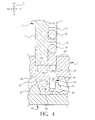
- Fig. 4 is a magnified view of the area designated "B" in Fig. 3, with the connector module and the base member shown in Figs. 2 and 3 in an assembled state;
- Fig. 5 is a side view of an alternative embodiment of the connector module shown in Fig. 2; and
- Fig. 6 is a side view of a conventional right-angle electrical connector.
-
- Figures 1-4 depict a presently-preferred surface-mounted right-angle
electrical connector 10. Each of the figures referred to throughout the specification is referenced to acommon coordinate system 8 depicted therein. Theelectrical connector 10 is adapted to be mounted on a circuit substrate such as a printed wireboard (PWB) 19. Theelectrical connector 10 adapted to mate with a second electrical connector, another circuit substrate, or a backplane (not shown). Theelectrical connector 10 is described in detail herein for exemplary purposes only, as the invention can be applied to virtually any type of right-angle connector. Certain features of theelectrical connector 10 are also described in a co-pending application filed on November 20, 2001 and titled "Pin-Grid-Array Electrical Connector," which is incorporated herein by reference in its entirety. - The
electrical connector 10 comprises abase member 11, a plurality ofconnector modules 12, and ahousing 13. The housing includes amain portion 13a and aforward portion 13b (see Figure 1). Thebase member 11 is adapted to be mounted on a surface of thePWB 19, as explained in detail below. Theconnector modules 12 are substantially enclosed by thehousing 13, and are mounted on thebase member 11. - Each
connector module 12 comprises aplate member 17, a plurality ofsignal conducting members 20, and a plurality of ground conducting members 21 (see Figure 2). Eachsignal conducting member 20 comprises amating pin 24, alead portion 26, and acontact portion 28. A first end of thelead portion 26 is mechanically and electrically coupled to thecontact portion 28, and an opposing second end of thelead portion 26 is mechanically and electrically coupled to themating pin 24. This arrangement forms an electrical path between themating pin 24 and thecontact portion 28. - Each of the
contact portions 28 preferably has a substantially rectangular cross-section. Thelead portions 26 each include one or more bends that cause themating pin 24 and thecontact portion 28 to extend in substantially perpendicular directions, i.e., themating pin 24 extends substantially in the "x" direction, and thecontact portion 28 extends substantially in the "y" direction (see Figure 2). - Each
ground conducting member 21 comprises a lead portion 30 (see Figure 2). A first end of eachlead portion 30 is mechanically and electrically coupled to acontact portion 32. An opposing second end of eachlead portion 30 is mechanically coupled to amating pin 34. This arrangement electrically couples thecontact portion 32 and themating pin 34. Each of thecontact portions 32 preferably has a substantially rectangular cross-section (other cross-sectional shapes, e.g., circular or conical, can also be used). Thelead portions 30 each include one or more bends that cause the mating pins 34 and thecontact portions 32 to extend in substantially perpendicular directions, i.e., the mating pins 34 extend substantially in the "x" direction, and thecontact portions 32 extend substantially in the "y" direction." - Each
plate member 17 is formed from an electrically insulative material such as plastic. Theplate members 17 each have a substantially planarforward surface 17a and a substantially planarlower surface 17b (see Figure 2). Theforward surface 17a and thelower surface 17b are substantially perpendicular. Theplate member 17 has a plurality ofgrooves 35 formed therein (see Figure 3; thegrooves 35 are not depicted in Figure 2, for clarity). Thegrooves 35 extend between theforward surface 17a and thelower surface 17b, and receive therespective lead portions members 20 and theground members 30. This arrangement causes the mating pins 24, 34 to extend away from theforward surface 17a of theplate member 17; thecontact portions lower surface 17b of theplate member 17. Alternative embodiments of theplate members 17 may accommodate more or less than the six conductingmembers 20 and sixground conducting members 21 positioned within eachplate member 17. - It should be noted that directional terms such as "upper," "lower," etc., are used with reference to the component orientations depicted in Figures 1-4; these terms are used for illustrative purposes only and, unless expressly stated otherwise, are not intended to limit the scope of the appended claims.
- The exemplary
electrical connector 10 includes six of theconnector modules 12 disposed in a side-by-side arrangement within thehousing 13. In other words, theconnector modules 12 are positioned so that theforward surfaces 17a of theplate members 17 are substantially co-planar, and thelower surfaces 17b of theplate members 17 are also substantially co-planar. Thecontact portions main portion 13a of thehousing 13. The significance of this feature is discussed below. - The
forward portion 13b of thehousing 13 encloses the mating pins 24, 34 (see figure 1). The mating pins 24, 34 are each adapted to engage a respective a female receptacle on another connector, a circuit substrate (other than the PWB 19), or a backplane. - The
connector modules 12 are mechanically and electrically coupled to thePWB 19 by way of thebase member 11. Thebase member 11 comprises amain portion 18. Themain portion 18 has anupper surface 18a that partially receives theplate members 17, and a substantially planarsecond surface 18b. Thebase member 11 further comprises a plurality ofstud members 22 projecting from thesecond surface 18b. Thestud members 22 and themain portion 18 are formed from an insulative material such a plastic, and most preferably are formed from liquid crystal polymer (LCP). Thestud members 22 and themain portion 18 are preferably formed on a unitary basis. Eachstud member 22 has an inner, or recessedsurface portion 22a that defines a recess 40 (see Figures 3 and 4). The significance of this feature is explained below. - The
upper surface 18a of thebase member 18 defines a plurality of slots 33 (see Figure 3). Theslots 33 each extend substantially in the longitudinal ("x") direction, along substantially an entire length of thebase member 18. A bottom of eachslot 33 is defined by a surface portion 18a1 of theupper surface 18a - Each of the
slots 33 is sized to partially receive a respective one of theplate members 17. In particular, each of theslots 33 has a width ("z" dimension) and a length ("x" dimension) approximately equal to a respective width and length of eachplate member 17. Eachslot 33 is thus adapted to receive and securely engage a bottom portion of arespective plate member 17 by way of a press fit. In other words, a bottom portion of eachplate member 17 is pressed into a respective one of theslots 33 so that thebottom surface 17b of theplate member 17 abuts the surface portion 18a1 of thebase member 11, thereby securing theplate member 17 to thebase member 11. (Other suitable means of securing theplate members 17 to thebase member 11 can be used instead of a press fit.) - A plurality of through
holes 32 are formed in the base member 11 (see Figure 3). Each throughhole 32 is defined by arespective surface portion 18c in themain portion 18. The through holes 32 each extend from the surface portion 18a1 to arespective stud member 22. Each throughhole 32 adjoins arespective recess 40. Each corresponding throughhole 32 andrecess 40 form apassage 42 that extends through themain portion 18 and therespective stud member 22. Thepassage 42 is adapted to receive at least a portion of acontact portion contact portions 32, 36 are each substantially aligned with, and extend into arespective passage 42 when theplate members 17 are positioned on thebase member 11. Further details concerning thepassages 42 are presented below. - The
surface portions 18c and thestud members 22 are at least partially covered with aconductive coating 44. (The thickness of the conductive coating is exaggerated in the figures, for clarity.) Theconductive coating 44 is a metallized layer that establishes electrical contact between thecontact portions 32, 36 and thePWB 19, as explained in detail below. Thecoating 44 is preferably formed from copper (Cu), nickel (Ni), and tin (Sn). Thecoating 44 is applied by activating thesecond surface 18b of themain portion 18 and a lower end of thesurface portion 18c with electroless CU. The recessedsurface portion 22a of thestud member 22 are also activated with the electroless CU. A 20-25-micron layer of electrolytic CU, a 4-6-micron layer of electrolytic Ni, and a 4-6 micron layer of electrolytic Sn are then sequentially applied to the activated areas. - A substantial portion of the Sn layer located on the
second surface 17b is subsequently removed by laser oblation, and the underling layers of Cu and Ni are removed by chemical etching. Thecoating 44 that remains after this process forms a substantially contiguous metallized layer on and immediately surrounding eachstud member 22. In particular, thecoating 44 associated with eachstud member 22 covers anouter surface 22b and the recessedsurface portion 22a of thestud member 22, a portion of thesecond surface 18b immediately adjacent theouter surface 22b, and the lower end of eachsurface portion 18c. - It should be noted that specific details relating to the composition and application of the
coating 44 are presented for exemplary purposes only; thecoating 44 can be formed from virtually any type of suitable conductive material applied in any conventional manner. - The
passages 42 are each adapted to receive at least a portion of one of thecontact portions 32, 36, as noted above. A minimal clearance, e.g., 0.001 inch, preferably exists between each signal orcontact portion 32, 36 and thecoating 44 when thecontact portions 32, 36 are positioned within thepassages 42. - The
PWB 19 includes a plurality of electrical traces that each terminate in a respectiveelectrical connection point 19a (see Figure 4). Theelectrical connector 10 is mechanically and electrically coupled to thePWB 19 by a mass soldering process, e.g., wave soldering, that forms a solder joint 23 between eachstud member 22 and a correspondingelectrical connection point 19a (see Figure 4; the solder joints 23 are not depicted in Figures 1 or 3, for clarity). - The
base member 11 preferably includes at least one stud-member support 22c. The stud-member support 22c does not have a signal orcontact portion 32, 36 disposed therein. The stud-member support 22c functions a guide for precisely positioning theelectrical connector 10 on thePWB 19 as theelectrical connector 10 is secured to thePWB 19. - The mechanical and electrical connections between the
electrical connector 10 and thePWB 19 are facilitated by theconductive coating 44. More specifically, the solder joints 23 securely bond theelectrical connection points 19a to theconductive coating 44 on therespective stud members 22, thereby securing theelectrical connector 10 to thePWB 19. Furthermore, theconductive coating 44, in conjunction with the solder joints 23, forms an electrically-conductive path between theelectrical connection points 19a and therespective contact portions - The
electrical connector 10 provides substantial advantages in relation to conventional surface-mounted right-angle connectors. For example, theelectrical connector 10 provides the advantages of surface-mounted connectors, e.g., compact size, while avoiding the difficulties usually associated with precisely positioning such connectors on a mounting surface. In particular, the stud-member supports 22c permit theelectrical connector 10 to be precisely aligned with a predetermined position on thePWB 19 when theelectrical connector 10 is installed on thePWB 19. This feature facilitates optimal electrical contact between theelectrical connection points 19a on thePWB 19, and therespective conducting members electrical connector 10. In addition, forming thestud members 22 as part of aunitary base member 11 facilitates a relatively high degree of co-planarity among thestud members 22, further optimizing the electrical contact between theelectrical connection points 19a and the conductingmembers - It is to be understood that even though numerous characteristics and advantages of the present invention have been set forth in the foregoing description, together with details of the structure and function of the invention, the disclosure is illustrative only, and changes may be made in detail, especially in matters of shape, size, and arrangement of the parts, within the principles of the invention to the full extent indicated by the broad general meaning of the terms in which the appended claims are expressed. For example, alternative configurations for the
stud members 22 are set forth in the co-pending application filed on November 20, 2001 and titled "Pin-Grid-Array Electrical Connector" which, as previously noted, is incorporated herein by reference in its entirety. Furthermore, the mating pins 24, 34 of theelectrical connector 10 can be replaced with female receptacles, i.e., theelectrical connector 10 can be adapted to mate with a complementary pin connector. - Figure 5 depicts
connector module 50. Theconnector module 50 represents an alternative embodiment of theconnector module 12. Components of theconnector module 50 that are substantially identical to those of theconnector module 12 are denoted by common reference numerals. Theconnector module 50 comprises aplate member 52 havingstud members 22 formed on alower surface 52a thereof. Theconnector module 52 is thus adapted to mount directly on a circuit substrate such as thePWB 19. In other words, theconnector module 50 mounts on thePWB 19 without the use of a base member such as thebase member 11 of theelectrical connector 10.
Claims (19)
- An electrical connector (10), comprising an electrically insulative base member (11) having a first upper surface (18a), a substantially planar second surface(18b), and a plurality of stud members (22) projecting from the second surface, the base member having a plurality of through holes (32) formed therein, the through holes each extending from the first surface to a respective stud member, an electrically-insulative plate member (17) mounted on the base member,
characterized in that a conducting member (20, 21) comprising a lead portion (26, 30) at least partially disposed within the plate member (17) and a contact portion (28, 32) at least partially disposed within the stud member (22). - The electrical connector according to claim 1, characterized in that the stud member has an outer surface and an inner surface, the inner surface (22a) defining a recess (40) that adjoins the first through hole (32) and is adapted to at least partially receive the contact portion (28, 32).
- The electrical connector according to claim 1, characterized in that at least a portion of the outer and the inner surfaces of the stud member are coated with a substantially contiguous layer of the electrically conductive material (44).
- The electrical connector according to claim 1, characterized in that the first upper surface (18a) of the base member defines a slot (33) for receiving a portion of the plate member (17).
- The electrical connector according to claim 1, characterized in that the conducting member (20, 21) further comprises a mating pin (24, 34) mechanically and electrically coupled to the lead portion (26, 30).
- The electrical connector according to claim 1, characterized in that the contact portion (28, 32) has a substantially rectangular cross section.
- The electrical connector according to claim 1, characterized in that the base member (11) further comprises a main portion (18) unitarily formed with the stud members (22).
- The electrical connector according to claim 5, characterized in that the mating pin (24, 34) and the contact portion (26, 32) extend in substantially perpendicular directions.
- The electrical connector according to claim 1, characterized in that at least a portion of the through hole (32) is coated with a substantially contiguous layer of the electrically conductive material (44).
- The electrical connector according to claim 1, characterized in that the base member is formed from liquid crystal polymer.
- The electrical connector according to claims 2 and 9, characterized in that the conductive coating comprises copper, nickel, and tin.
- The electrical connector according to claim 11, characterized in that the conductive coating comprises a layer of the copper approximately twenty to approximately twenty-five microns thick, a layer of the nickel approximately four to approximately six microns thick, and a layer of the tin approximately four to approximately six microns thick.
- The electrical connector according to claim 1, characterized in that the base member (18) further comprises a stud-member (22) support projecting from the second surface (18b).
- The electrical connector according to claim 1, characterized in that it further comprises a housing (13), wherein the plate member (17) is at least partially disposed within the housing.
- The electrical connector according to claim 14, characterized in that the housing comprises a main portion (13a) and a forward portion (13b).
- The electrical connector according to claim 1, characterized in that the plate (17) has a plurality of grooves (30) formed therein for receiving the lead portion (26, 30) of the conducting member (20, 21).
- A right-angle electrical connector characterized bya plurality of conducting members (20, 21) each comprising a contact portion (28, 32) and a lead portion (26, 30) electrically coupled to the contact portion;a plurality of plate members (17) disposed within the housing (13), each of the plate members having a plurality of grooves (30) formed therein for receiving the lead portions; anda base member (11) having a plurality of slots (33) formed in a first surface (18a) thereof for receiving and retaining the plate members and a plurality of stud members (22) projecting from a second surface (18b) thereof and being adapted to mount on a circuit substrate (19), the base member receiving each of the contact portions (28, 32) in respective passages (42) formed therein and extending through the stud members (22), and the contact portions are adapted to be electrically coupled to the circuit substrate by a conductive coating (44) disposed on at least a portion of each of the stud members.
- A right-angle connector according to claim 17 characterized in that the plurality of conducting members comprises at least one of a signal conducting member (20) and at least one of a ground conducting member (21).
- A right-angle connector according to claim 17 comprising the plurality of electrically insulative plate members (17) each having a first surface, a substantially perpendicular second surface, and the plurality of stud members projecting from the second surface and at least partially covered by an electrically-conductive coating and adapted to be mounted on a circuit substrate
characterized in that
the conducting members each extend between one of the first surfaces and one of the stud members, and each of the contact portions is at least partially disposed within a respective one of the stud members and is adapted to be electrically coupled to the circuit substrate by the conductive coating.
Applications Claiming Priority (2)
| Application Number | Priority Date | Filing Date | Title |
|---|---|---|---|
| US989646 | 2001-11-20 | ||
| US09/989,646 US6666693B2 (en) | 2001-11-20 | 2001-11-20 | Surface-mounted right-angle electrical connector |
Publications (1)
| Publication Number | Publication Date |
|---|---|
| EP1315245A1 true EP1315245A1 (en) | 2003-05-28 |
Family
ID=25535318
Family Applications (1)
| Application Number | Title | Priority Date | Filing Date |
|---|---|---|---|
| EP02025634A Withdrawn EP1315245A1 (en) | 2001-11-20 | 2002-11-19 | Surface-mounted right-angle electrical connector |
Country Status (7)
| Country | Link |
|---|---|
| US (1) | US6666693B2 (en) |
| EP (1) | EP1315245A1 (en) |
| JP (1) | JP2003197299A (en) |
| KR (1) | KR20030041797A (en) |
| CN (1) | CN1287488C (en) |
| CA (1) | CA2410742A1 (en) |
| TW (1) | TWI221683B (en) |
Families Citing this family (20)
| Publication number | Priority date | Publication date | Assignee | Title |
|---|---|---|---|---|
| JP2006515705A (en) * | 2002-05-06 | 2006-06-01 | モレックス インコーポレーテッド | Differential signal connector with electrostatic discharge protection function |
| US7226298B1 (en) | 2006-03-29 | 2007-06-05 | Fci Americas Technology, Inc. | Electrical connector with segmented housing |
| JP4833733B2 (en) * | 2006-05-18 | 2011-12-07 | 古河電気工業株式会社 | Wiring board unit |
| US7316585B2 (en) * | 2006-05-30 | 2008-01-08 | Fci Americas Technology, Inc. | Reducing suck-out insertion loss |
| US7553170B2 (en) * | 2006-12-19 | 2009-06-30 | Fci Americas Technology, Inc. | Surface mount connectors |
| US8366485B2 (en) | 2009-03-19 | 2013-02-05 | Fci Americas Technology Llc | Electrical connector having ribbed ground plate |
| US8231415B2 (en) | 2009-07-10 | 2012-07-31 | Fci Americas Technology Llc | High speed backplane connector with impedance modification and skew correction |
| EP2624034A1 (en) | 2012-01-31 | 2013-08-07 | Fci | Dismountable optical coupling device |
| US8944831B2 (en) | 2012-04-13 | 2015-02-03 | Fci Americas Technology Llc | Electrical connector having ribbed ground plate with engagement members |
| USD727852S1 (en) | 2012-04-13 | 2015-04-28 | Fci Americas Technology Llc | Ground shield for a right angle electrical connector |
| US9257778B2 (en) | 2012-04-13 | 2016-02-09 | Fci Americas Technology | High speed electrical connector |
| USD718253S1 (en) | 2012-04-13 | 2014-11-25 | Fci Americas Technology Llc | Electrical cable connector |
| USD727268S1 (en) | 2012-04-13 | 2015-04-21 | Fci Americas Technology Llc | Vertical electrical connector |
| USD751507S1 (en) | 2012-07-11 | 2016-03-15 | Fci Americas Technology Llc | Electrical connector |
| US9543703B2 (en) | 2012-07-11 | 2017-01-10 | Fci Americas Technology Llc | Electrical connector with reduced stack height |
| USD745852S1 (en) | 2013-01-25 | 2015-12-22 | Fci Americas Technology Llc | Electrical connector |
| USD720698S1 (en) | 2013-03-15 | 2015-01-06 | Fci Americas Technology Llc | Electrical cable connector |
| US9585263B2 (en) * | 2014-10-15 | 2017-02-28 | Continental Automotive Systems, Inc. | Pin to PCB connection structure and method |
| TWI685150B (en) * | 2014-12-05 | 2020-02-11 | 美商司固科技公司 | High profile electrical connector |
| JP7076298B2 (en) * | 2018-06-21 | 2022-05-27 | ヒロセ電機株式会社 | Right angle electrical connector |
Citations (3)
| Publication number | Priority date | Publication date | Assignee | Title |
|---|---|---|---|---|
| US4875862A (en) * | 1987-09-09 | 1989-10-24 | Murata Manufacturing Co., Ltd. | Surface mountable connector |
| US5688130A (en) * | 1996-04-10 | 1997-11-18 | Molex Incorporated | Electrical connector assembly for pc cards |
| US6083047A (en) * | 1997-01-16 | 2000-07-04 | Berg Technology, Inc. | Modular electrical PCB assembly connector |
Family Cites Families (18)
| Publication number | Priority date | Publication date | Assignee | Title |
|---|---|---|---|---|
| US3885076A (en) | 1973-05-09 | 1975-05-20 | Bell Telephone Labor Inc | Electron beam generated patterns of metal-containing polymers |
| JPS6263683A (en) | 1985-09-13 | 1987-03-20 | Ube Ind Ltd | Method for forming a plating layer with a pattern |
| US4882633A (en) | 1987-01-09 | 1989-11-21 | Canon Kabushiki Kaisha | Video signal reproducing apparatus with memory |
| US4882200A (en) | 1987-05-21 | 1989-11-21 | General Electric Company | Method for photopatterning metallization via UV-laser ablation of the activator |
| US5227588A (en) | 1991-03-25 | 1993-07-13 | Hughes Aircraft Company | Interconnection of opposite sides of a circuit board |
| EP0693795B1 (en) | 1994-07-22 | 1999-03-17 | Berg Electronics Manufacturing B.V. | Selectively metallizized connector with at least one coaxial or twinaxial terminal |
| EP0693796A1 (en) | 1994-07-22 | 1996-01-24 | Connector Systems Technology N.V. | Connector provided with metal strips as contact members, connector assembly comprising such a connector |
| EP0694996A1 (en) | 1994-07-22 | 1996-01-31 | Connector Systems Technology N.V. | Selectively metallized plastic hold-down connector |
| US6249048B1 (en) | 1997-03-21 | 2001-06-19 | Siemens N.V. | Polymer stud grid array |
| ATE194249T1 (en) | 1994-09-23 | 2000-07-15 | Siemens Nv | POLYMER STUD GRID ARRAY PACKAGE |
| DE4438872C1 (en) | 1994-11-03 | 1995-12-07 | Harting Elektronik Gmbh | Coaxial angle connector for PCB |
| TW267265B (en) | 1995-06-12 | 1996-01-01 | Connector Systems Tech Nv | Low cross talk and impedance controlled electrical connector |
| ES2163043T3 (en) | 1995-10-16 | 2002-01-16 | Siemens Nv | POLYMER HIGHLIGHTS GRID MATRIX. |
| DE59608615D1 (en) | 1995-10-16 | 2002-02-28 | Siemens Nv | POLYMER BUMPER MATRIX HOUSING FOR MICROWAVE CIRCUIT ARRANGEMENTS |
| US5766043A (en) * | 1996-02-29 | 1998-06-16 | Corcom, Inc. | Telephone connector |
| US6241535B1 (en) | 1996-10-10 | 2001-06-05 | Berg Technology, Inc. | Low profile connector |
| US6042389A (en) | 1996-10-10 | 2000-03-28 | Berg Technology, Inc. | Low profile connector |
| US6183301B1 (en) | 1997-01-16 | 2001-02-06 | Berg Technology, Inc. | Surface mount connector with integrated PCB assembly |
-
2001
- 2001-11-20 US US09/989,646 patent/US6666693B2/en not_active Expired - Fee Related
-
2002
- 2002-10-31 CA CA002410742A patent/CA2410742A1/en not_active Abandoned
- 2002-11-13 TW TW091133265A patent/TWI221683B/en not_active IP Right Cessation
- 2002-11-19 KR KR1020020071829A patent/KR20030041797A/en not_active Ceased
- 2002-11-19 EP EP02025634A patent/EP1315245A1/en not_active Withdrawn
- 2002-11-20 CN CN02151394.5A patent/CN1287488C/en not_active Expired - Fee Related
- 2002-11-20 JP JP2002336929A patent/JP2003197299A/en active Pending
Patent Citations (3)
| Publication number | Priority date | Publication date | Assignee | Title |
|---|---|---|---|---|
| US4875862A (en) * | 1987-09-09 | 1989-10-24 | Murata Manufacturing Co., Ltd. | Surface mountable connector |
| US5688130A (en) * | 1996-04-10 | 1997-11-18 | Molex Incorporated | Electrical connector assembly for pc cards |
| US6083047A (en) * | 1997-01-16 | 2000-07-04 | Berg Technology, Inc. | Modular electrical PCB assembly connector |
Also Published As
| Publication number | Publication date |
|---|---|
| JP2003197299A (en) | 2003-07-11 |
| CA2410742A1 (en) | 2003-05-20 |
| KR20030041797A (en) | 2003-05-27 |
| TWI221683B (en) | 2004-10-01 |
| US6666693B2 (en) | 2003-12-23 |
| US20030096516A1 (en) | 2003-05-22 |
| CN1287488C (en) | 2006-11-29 |
| CN1421959A (en) | 2003-06-04 |
| TW200303633A (en) | 2003-09-01 |
Similar Documents
| Publication | Publication Date | Title |
|---|---|---|
| US6666693B2 (en) | Surface-mounted right-angle electrical connector | |
| KR101353650B1 (en) | Composite contact for fine pitch electrical interconnect assembly | |
| CN1067178C (en) | Circuit board and edge-mountable conenctor therefor, and method of preparing a circuit board edge | |
| US6527588B2 (en) | Electrical connector with integrated PCB assembly | |
| US7497695B2 (en) | Connection structure for printed wiring board | |
| CN2749079Y (en) | Electric connector | |
| US7125260B2 (en) | Mounting structure of connector | |
| US7695289B1 (en) | Connector | |
| EP0918376A2 (en) | Modular connectors | |
| US7025640B2 (en) | Circuit board inter-connection system and method | |
| US6776623B1 (en) | Transceiver mounting adapters | |
| US6638082B2 (en) | Pin-grid-array electrical connector | |
| US6328577B1 (en) | High density electric connector set | |
| EP0898326A2 (en) | Method of fabricating electronic device employing a flat flexible circuit and including the device itself | |
| KR19990045505A (en) | Terminal blades mounted on flexible board | |
| US6551134B1 (en) | Mounted transceivers | |
| EP0906005A1 (en) | Terminal pins mounted in flexible substrates | |
| JPH08102348A (en) | PCB connector | |
| CN121368065A (en) | Circuit board assembly, manufacturing method thereof and electronic equipment |
Legal Events
| Date | Code | Title | Description |
|---|---|---|---|
| PUAI | Public reference made under article 153(3) epc to a published international application that has entered the european phase |
Free format text: ORIGINAL CODE: 0009012 |
|
| AK | Designated contracting states |
Designated state(s): AT BE BG CH CY CZ DE DK EE ES FI FR GB GR IE IT LI LU MC NL PT SE SK TR |
|
| AX | Request for extension of the european patent |
Extension state: AL LT LV MK RO SI |
|
| 17P | Request for examination filed |
Effective date: 20030929 |
|
| AKX | Designation fees paid |
Designated state(s): AT BE BG CH CY CZ DE DK EE ES FI FR GB GR IE IT LI LU MC NL PT SE SK TR |
|
| STAA | Information on the status of an ep patent application or granted ep patent |
Free format text: STATUS: THE APPLICATION HAS BEEN WITHDRAWN |
|
| 18W | Application withdrawn |
Effective date: 20080606 |