EP1315244A1 - Low profile high density sockets and related method of manufacturing - Google Patents
Low profile high density sockets and related method of manufacturing Download PDFInfo
- Publication number
- EP1315244A1 EP1315244A1 EP03001369A EP03001369A EP1315244A1 EP 1315244 A1 EP1315244 A1 EP 1315244A1 EP 03001369 A EP03001369 A EP 03001369A EP 03001369 A EP03001369 A EP 03001369A EP 1315244 A1 EP1315244 A1 EP 1315244A1
- Authority
- EP
- European Patent Office
- Prior art keywords
- contact
- spacer
- bar
- spacer bar
- connector
- Prior art date
- Legal status (The legal status is an assumption and is not a legal conclusion. Google has not performed a legal analysis and makes no representation as to the accuracy of the status listed.)
- Granted
Links
- 238000004519 manufacturing process Methods 0.000 title claims description 7
- 125000006850 spacer group Chemical group 0.000 claims abstract description 101
- 239000013536 elastomeric material Substances 0.000 claims abstract description 5
- 238000000034 method Methods 0.000 claims description 15
- 238000003780 insertion Methods 0.000 claims description 2
- 230000037431 insertion Effects 0.000 claims description 2
- 230000008030 elimination Effects 0.000 abstract 1
- 238000003379 elimination reaction Methods 0.000 abstract 1
- 229920001971 elastomer Polymers 0.000 description 4
- MINPZZUPSSVGJN-UHFFFAOYSA-N 1,1,1,4,4,4-hexachlorobutane Chemical compound ClC(Cl)(Cl)CCC(Cl)(Cl)Cl MINPZZUPSSVGJN-UHFFFAOYSA-N 0.000 description 3
- AGCPZMJBXSCWQY-UHFFFAOYSA-N 1,1,2,3,4-pentachlorobutane Chemical compound ClCC(Cl)C(Cl)C(Cl)Cl AGCPZMJBXSCWQY-UHFFFAOYSA-N 0.000 description 3
- 101150049492 DVR gene Proteins 0.000 description 3
- 239000004020 conductor Substances 0.000 description 3
- 239000000806 elastomer Substances 0.000 description 3
- 239000000463 material Substances 0.000 description 3
- 239000012811 non-conductive material Substances 0.000 description 3
- 230000003044 adaptive effect Effects 0.000 description 2
- 238000005530 etching Methods 0.000 description 2
- 239000002184 metal Substances 0.000 description 2
- 239000000758 substrate Substances 0.000 description 2
- 229910000906 Bronze Inorganic materials 0.000 description 1
- OAICVXFJPJFONN-UHFFFAOYSA-N Phosphorus Chemical compound [P] OAICVXFJPJFONN-UHFFFAOYSA-N 0.000 description 1
- 238000004026 adhesive bonding Methods 0.000 description 1
- 229910045601 alloy Inorganic materials 0.000 description 1
- 239000000956 alloy Substances 0.000 description 1
- 238000003491 array Methods 0.000 description 1
- 239000010974 bronze Substances 0.000 description 1
- KUNSUQLRTQLHQQ-UHFFFAOYSA-N copper tin Chemical compound [Cu].[Sn] KUNSUQLRTQLHQQ-UHFFFAOYSA-N 0.000 description 1
- 230000008878 coupling Effects 0.000 description 1
- 238000010168 coupling process Methods 0.000 description 1
- 238000005859 coupling reaction Methods 0.000 description 1
- 230000000694 effects Effects 0.000 description 1
- 239000012777 electrically insulating material Substances 0.000 description 1
- 230000006698 induction Effects 0.000 description 1
- 230000014759 maintenance of location Effects 0.000 description 1
- 230000007246 mechanism Effects 0.000 description 1
- 238000012986 modification Methods 0.000 description 1
- 230000004048 modification Effects 0.000 description 1
- 230000008569 process Effects 0.000 description 1
- 230000000135 prohibitive effect Effects 0.000 description 1
- 239000012858 resilient material Substances 0.000 description 1
- 229910000679 solder Inorganic materials 0.000 description 1
- 239000007787 solid Substances 0.000 description 1
- 238000006467 substitution reaction Methods 0.000 description 1
- -1 such as Substances 0.000 description 1
- 238000010618 wire wrap Methods 0.000 description 1
Images






Classifications
-
- H—ELECTRICITY
- H01—ELECTRIC ELEMENTS
- H01R—ELECTRICALLY-CONDUCTIVE CONNECTIONS; STRUCTURAL ASSOCIATIONS OF A PLURALITY OF MUTUALLY-INSULATED ELECTRICAL CONNECTING ELEMENTS; COUPLING DEVICES; CURRENT COLLECTORS
- H01R13/00—Details of coupling devices of the kinds covered by groups H01R12/70 or H01R24/00 - H01R33/00
- H01R13/02—Contact members
- H01R13/22—Contacts for co-operating by abutting
- H01R13/24—Contacts for co-operating by abutting resilient; resiliently-mounted
- H01R13/2407—Contacts for co-operating by abutting resilient; resiliently-mounted characterized by the resilient means
- H01R13/2414—Contacts for co-operating by abutting resilient; resiliently-mounted characterized by the resilient means conductive elastomers
-
- H—ELECTRICITY
- H01—ELECTRIC ELEMENTS
- H01R—ELECTRICALLY-CONDUCTIVE CONNECTIONS; STRUCTURAL ASSOCIATIONS OF A PLURALITY OF MUTUALLY-INSULATED ELECTRICAL CONNECTING ELEMENTS; COUPLING DEVICES; CURRENT COLLECTORS
- H01R12/00—Structural associations of a plurality of mutually-insulated electrical connecting elements, specially adapted for printed circuits, e.g. printed circuit boards [PCB], flat or ribbon cables, or like generally planar structures, e.g. terminal strips, terminal blocks; Coupling devices specially adapted for printed circuits, flat or ribbon cables, or like generally planar structures; Terminals specially adapted for contact with, or insertion into, printed circuits, flat or ribbon cables, or like generally planar structures
- H01R12/70—Coupling devices
- H01R12/7082—Coupling device supported only by cooperation with PCB
-
- H—ELECTRICITY
- H01—ELECTRIC ELEMENTS
- H01R—ELECTRICALLY-CONDUCTIVE CONNECTIONS; STRUCTURAL ASSOCIATIONS OF A PLURALITY OF MUTUALLY-INSULATED ELECTRICAL CONNECTING ELEMENTS; COUPLING DEVICES; CURRENT COLLECTORS
- H01R12/00—Structural associations of a plurality of mutually-insulated electrical connecting elements, specially adapted for printed circuits, e.g. printed circuit boards [PCB], flat or ribbon cables, or like generally planar structures, e.g. terminal strips, terminal blocks; Coupling devices specially adapted for printed circuits, flat or ribbon cables, or like generally planar structures; Terminals specially adapted for contact with, or insertion into, printed circuits, flat or ribbon cables, or like generally planar structures
- H01R12/50—Fixed connections
- H01R12/51—Fixed connections for rigid printed circuits or like structures
- H01R12/52—Fixed connections for rigid printed circuits or like structures connecting to other rigid printed circuits or like structures
Definitions
- the present invention relates to electrical connectors and relates more particularly to high density electrical connectors used to interconnect electrical components such as land grid array (LGA) packages, ball grid array (BGA) packages, single in-line type modules, or other possible configurations.
- LGA land grid array
- BGA ball grid array
- High density electrical connectors adapted to be disposed for example, intermediate a pair of parallel circuit board units for establishing electrical connections therebetween, are old. Examples of such devices are as follows:
- U.S. Patent N°. 3,638,163, issued on 1/25/72 to Loosme discloses a connector made from a N°nconductive resilient tube and contacts which are equally spaced longitudinally along the cylindrical surface of the tube.
- U.S. Patent N°. 3,795,884, issued on 3/5/74 to Kotaka discloses an electrical connector having a coil spring, the turns of which serve as conductors extending between terminal pads on PC boards.
- U.S. Patent N°. 3,818,414, issued on 6/18/74 to Davies et al. discloses electrical connectors which have support members having a spiral groove into which C-shaped conductive members are formed by wire wrapping and gluing.
- U.S. Patent N°. 3, 858, 958, issued on 1/07/75 to Davies discloses electrical connectors in which a solid cylinder of elastomer provides a common support for rings contacts. Contacts are formed by etching of a phosphor bronze tube and secured to the elastomer.
- U.S. Patent N°. 3,951,493, issued on 4/20/76 to Kozel et al. discloses a connector in which an elongated non-conductive tubular-like member of resilient material is provided and about which is wound and secured a continuous strip of conductive material.
- U.S. Patent N°. 4,421,370, issued on 12/20/83 to Treakle et al. discloses cylindrical contacts which have a hole for receiving a supporting thread and a plastic boat for supporting the contacts.
- U.S. Patent N°. 4,952,156, issued on 8/28/90 to Schmedding discloses a connector having a plurality of contact terminals wherein the contact terminals are each crimped onto a continuous length of electrically insulating material.
- Still a further objection of the invention is to provide a device and method of the aforementioned type wherein such a device is capable of being fabricated with ease of manufacture and relatively little additional labor costs.
- the invention relates to a method and related assembly for fabricating a connector with plural contacts arranged in an array which can readily be varied in row position from row to row depending on the arrangement of contacts on opposed contact plate surfaces between which the connector is inserted.
- the invention involves an electrical connector for connecting contacts disposed between two spaced apart contact surfaces and comprises a frame having at least two opposed portions to define a space therebetween and at least one spacer bar supported on the frame within the space.
- the spacer bar has at least one separate contact element disposed in spatial arrangement therealong and has at least two non-conductive spacer elements disposed on either side of the contact element for positioning the at least one contact element in a given location along the spacer bar.
- the at least one spacer bar has a non conductive surface.
- the spacers are separate elements mountable on the spacer bar
- the spacer bar is an elongated length of elastomeric material having portions of narrowed diameter followed by larger diameter portions to define a series of bosses and gaps thereon and wherein the contact elements are disposed on the spacer bar between the bosses.
- the contact elements have an inner opening having a diameter which is slightly greater than the outer diameter of the spacer bar.
- the contact elements may be formed as split spiral rings each having a first and second free end which are laterally offset from one another allowing the rings to be radially compliant and the rings have an inner opening of a diameter which is slightly greater than the outer diameter of the spacer bar.
- the frame is a closed shape having opposed pairs of openings formed therein for receiving the at least one spacer bar therein and a retainer is associated with each of the opposed pairs of openings in the frame for securing a corresponding one of the spacer bars within the opening, and wherein the connector has a plurality of spacer bars supported on the frame.
- the invention also resides in a connector with a frame and a plurality of bars supported on the frame.
- a retainer is associated with the frame for holding each of the spacer bars on the frame against movement.
- Each of the spacer bars includes a plurality of contact elements slidingly disposed thereon and a plurality of spacer members disposed on opposite sides of each contact element locating each contact element in a position relative to the frame.
- the spacer members and the spacer bars are formed from a nonconductive material and the spacer members and the contact elements are movably disposed on the bars. Desirably, the contact elements are radially yieldably supported on the spacer bar.
- the invention further resides in a method of assembling an electrical connector for use in an array type contact grid comprising the steps of providing at least one elongate bar having a given outer diameter; providing a plurality of contact elements each having a hole formed therein defined generally by an inner diameter which is greater than the outer diameter of the spacer bar; providing a plurality of spacer members; placing a contact element onto the bar and spacing one contact element from another on the bar by placing one or more of the spacers therebetween and securing the at least one spacer bar with the contact elements and spacers thereon to the frame to hold the at least one spacer bar in place on the frame.
- the method further comprises providing each of the contact elements as a split ring capable of radially yielding inwardly and inserting the connector into a gap between two spaced apart contact plates and forming the gap such that upon insertion of the connector into the gap the contact elements are compressed.
- the invention further resides in a method of forming a spacer bar useable as a connection between circuit substrates comprising steps of providing a spacer bar made from an elastomeric material; stretching the spacer bar such that the bar becomes elongated and of a reduced diameter; and placing a contact member on the spacer bar.
- the method of forming a spacer bar further includes forming the spacer bar with a plurality of bosses separated from one another by gaps into which gaps, a contact member is placed.
- the invention also resides in a spacer bar made from an elastomeric material whereinthe spacer bar can be stretched such that the bar becomes elongated and of a reduced diameter so that a contact member can be placed on the stretched bar.
- the spacer bar is formed with a plurality of bosses separated from one another by gaps into which gaps, a contact member is placed.
- the array connector illustrated generally as 2 embodies the present invention.
- the connector array 2 is comprised of a frame 10, which has a generally closed shape but can incorporate any geometric shape.
- the frame is shown as a square, but could take the form for example, of a rectangle or circle.
- the array connector 2 could be inserted between two spaced apart electrical components 5, 5 having a plurality of conductive elements 7, 7' disposed on surfaces 9, 9' thereof for contact engagement with the contact elements on the connector 2.
- Conductive elements 7, 7' could be lands on a circuit substrate, solder masses on a BGA package or any other suitable arrangement.
- the connector array 2 further includes a plurality of contact elements 12,12 which are disposed along an elongated spacer bar 14,14 which at each end thereof is secured to the frame.
- Contacts 12, 12 are preferably stamped and formed from a sheet of suitably conductive material, such as cooper alloy.
- Disposed between each of the contact elements 12,12 is one or more of a plurality of spacers 16,16 which are made from an insulative material interposed between contact elements 12,12 to position each of the contact elements 12,12 in alignment with a juxtaposed one the surface contacts 7,7' disposed on corresponding ones of the contact plates 5,5'.
- the components 5, 5' engage opposite sides of connector 2. Any known clamping mechanism (not shown) can retain components 5, 5' in suitable electrical connection with connector 2.
- the frame 10 has a plurality of aligned holes 20, 20' which are aligned with each other along opposite frame members so as to be able to receive one of the plurality of connecting rods 16,16 therein.
- each spacer bar 14,14 is of a length such that each end thereof is journalled within one of the openings 20,20' to hold it in alignment within the frame 10 so that registration between the contact elements 12,12 of the connector 2 and the corresponding surface contacts 7,7 can be effected.
- each spacer bar 14,14 is made from a non-conductive material, such as, plastic or an anodized metal.
- These spacer bars can be generally of a uniform circular diameter and are rigid in character.
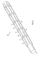
- a typical spacer bar of the invention is seen in Figures 8A-8C.
- each contact element 12 has a generally annular shape which is capable of compressing radially about the spacer bar 14.
- the spacer bar contact elements 12,12 are metal spring rings with an interior opening 30 having a diameter D1 which can be somewhat greater in diameter than the outer diameter OD (see Fig. 4) of the spacer bar 14.
- the spring contact elements 12,12 can take many different designs, but in the preferred embodiments they are split lock washers.
- the contact element 12' has N° offset, yet has an interrupted perimeter 19 making it radially yieldable.
- the contact element 12" has a continuous annulus, yet is wider and has a thinner gauge thereby making it yieldable.
- the contact element 12"' has a pleat 23 formed in its perimeter thereby allowing it to be yieldable.
- the contact element 12"" is a standard rigid washer and the diameter of its inner opening is such that the washer can tilt on the bar 14, e.g. yield, between fixed spacers 27,27 secured to the bar 14 from an unloaded condition (Fig. 3g) to a loaded condition (Fig. 3h).
- each contact element 12,12 has open ends 32,34, which are disposed in a side-by-side manner so as to be offset from one another in a non-engaging manner. Since the outer diameter OD of the spacer bar 14 is preferably smaller than the inner diameter D1 of the opening 30 of the contact element 12, the lateral offset OF between the ends 32 and 34 of the contact spring allows each contact spring when engaged by the parallel spaced apart contact plates 5,5' to be compressed radially about the corresponding one of the spacer bars 14,14 to which it is mounted to effect positive contact between one contact element 7 on one plate 5 and the corresponding contact element 7 on the opposite plate 5'.
- each spacer element is preferably made from an insulative material so as to electrically isolate adjacent contact elements from one another on the common spacer bar.
- Spacer 16 could be made, for example, from plastic or an elastomer. Since each spacer bar 14,14 is also made from a non-conductive material, each contact element 12,12 is positioned on each spacer bar 14 such that each is electrically isolated from the other contact elements 12 on the same bar.
- spacer elements 16,16' as shown in the embodiment of these figures, have a longitudinally extending slit 36 enabling it to be snap fitted over bar 14 and to be more versatile to adapt to varying and different diameters of the spacer bars and to accommodate manufacturing variation.
- spacer elements as shown in Figures 6 and 7 which have a complete and uninterrupted annulus, and thus have N° such longitudinal slot formed therein.
- the spacers of Fig. 6 and 7 have lengths L1 and L2, respectively, which could be different. Such differing lengths allow almost infinite combinations of spacings to be made between connector contact elements 12,12 to position each connector contact element 12 in registration with the corresponding pair (upper and lower ones of the conductive elements 7,7) on each of the oppositely disposed components 5,5'. Thus, by varying combinations of the spacers 16 and 16' positioning of the connector contact elements 12 can be infinitely effected. It should be further understood that each of the spacers 16,16' can be freely slidable along the spacer bar 14 about which it is disposed.
- Each opposed pair of openings 20,20 formed in the frame 10 of the array 2 slidably receives a spacer bar 14 therein.
- Each spacer bar 14 has a length L which is longer than the width dimension W of the frame 10 defined between opposed inner side faces of the frame 10.
- each spacer bar 14,14 can be inserted through one of the openings 20,20 in each opposed opening pair, and thereafter fed through the interior confine 13 of the frame. While each spacer bar is being pushed into the interior confine 13 of the frame, alternating contact elements 12,12 and spacers 16,16' are inserted over the fed length of the spacer bar in accordance with the specifications of the job. Once this is complete, the spacer bar assembly 25 provides the ends of the spacer bar 14 with a small uncovered length.
- the uncovered length remains within the corresponding one of the openings pairs in the frame.
- the outer faces 40,40 of the frame 10 in which the openings 20,20 are formed are capped by dowels or other like structure so as to secure the spacer rod against movement relative to the frame and within the confines 13.
- retention structure such as a cotter pin, could secure rod 16 in frame 10 as a suitable retainer.
- frame 10 could be formed from several components that are built up around rods 16.
- the assembly illustrated includes a spacer bar referenced generally as 50 and is formed from an elastometic material, such as rubber.
- Each such spacer bar 50 has integrally formed with it a plurality of spacer bosses 42,42 located along the length thereof.
- these bosses are of an outer diameter which is slightly larger than the inner diameters D1 of the contact elements 12,12, yet are smaller in diameter than the outer diameter circumference of each of the contact elements 12,12.
- the bosses 42,42 act to capture the contact element 12 disposed therebetween from unwanted axial movement within the gap between each boss.
- the assembly is fabricated by pulling the free ends 60,62 of the bar in the directions shown by the arrows to elongate it, and thereby reduce the outer diameter of the bosses. In so doing, one or more contact elements can be slid over the bosses until located in the designated gap defined by two consecutively spaced boss elements. Thereafter, the ends of the spacer bar can be released and the contact rims will be held in place thereon.
- Fig. 11 displays an alternative arrangement of the present invention.
- the frame 10 is used as a connection between two perpendicularly oriented circuit boards, namely, board PCB1 and PCB2. That is, the frame 10 is located relative to boards PCB1 and PCB2 such that PCB2 is received within gap 70 disposed between opposed rows of contact elements 12,12, while simultaneously, these contact elements are also in contact with corresponding contact surfaces 74 and 76 on board PCB1.
Landscapes
- Coupling Device And Connection With Printed Circuit (AREA)
- Manufacturing Of Electrical Connectors (AREA)
- Connector Housings Or Holding Contact Members (AREA)
Abstract
Description
- The present invention relates to electrical connectors and relates more particularly to high density electrical connectors used to interconnect electrical components such as land grid array (LGA) packages, ball grid array (BGA) packages, single in-line type modules, or other possible configurations.
- High density electrical connectors adapted to be disposed for example, intermediate a pair of parallel circuit board units for establishing electrical connections therebetween, are old. Examples of such devices are as follows:
- U.S. Patent N°. 3,638,163, issued on 1/25/72 to Loosme discloses a connector made from a N°nconductive resilient tube and contacts which are equally spaced longitudinally along the cylindrical surface of the tube.
- U.S. Patent N°. 3,795,884, issued on 3/5/74 to Kotaka discloses an electrical connector having a coil spring, the turns of which serve as conductors extending between terminal pads on PC boards.
- U.S. Patent N°. 3,818,414, issued on 6/18/74 to Davies et al. discloses electrical connectors which have support members having a spiral groove into which C-shaped conductive members are formed by wire wrapping and gluing.
- U.S. Patent N°. 3, 858, 958, issued on 1/07/75 to Davies discloses electrical connectors in which a solid cylinder of elastomer provides a common support for rings contacts. Contacts are formed by etching of a phosphor bronze tube and secured to the elastomer.
- U.S. Patent N°. 3,951,493, issued on 4/20/76 to Kozel et al. discloses a connector in which an elongated non-conductive tubular-like member of resilient material is provided and about which is wound and secured a continuous strip of conductive material.
- U.S. Patent N°. 4,421,370, issued on 12/20/83 to Treakle et al. discloses cylindrical contacts which have a hole for receiving a supporting thread and a plastic boat for supporting the contacts.
- U.S. Patent N°. 4,952,156, issued on 8/28/90 to Schmedding discloses a connector having a plurality of contact terminals wherein the contact terminals are each crimped onto a continuous length of electrically insulating material.
- It is also know from U.S. Patent N° 5,397,240 to utilize a connector with a highly dense arrangement adapted to be disposed intermediate a pair of parallel circuit members. Ring shaped contacts are compressed between pads located on the surface of each circuit members in order that the signal passes from one pad to the other pad. These ring-shaped contacts are disposed in recesses provided by isolating parts located on an electrically-conductive member which provides an electrical coupling between the two circuits and thus controls the impedance and aids in reducing crosstalk noise.
- In the above cited references, there can be seen numerous devices which connect within a contact array environment. However, the connectors disclosed in these prior art patents are problematic in that each do not address the heretofore known problem of varying contacts spacing, variations in pitch in orthogonal directions, implementation of missing contacts, joint grounding, and connectors of nonstandard shapes. Furthermore, the ability of these array connectors to vary and work with differing design options with respect to overall size, number of contacts in contact spacing is highly limited, if not entirely impossible. An example of difficulties linked to the manufacture of connectors using unstandard specification in matter of contact width, spacing, etc... is disclosed in U.S. Patent N° 3 858 958 referenced here above. From this teaching it appears that special patterns are determined during the etching process of a metallic tube. Even if such devices could be modified to accept a greater variety of different array contact settings, the cost associated with the fabrication of such adaptive connectors from standard production and labor costs would be prohibitive.
- Accordingly, it is an object of the invention to provide a highly versatile low induction contact array capable of being very tolerant of differences in contact spacing, number, size, height, pitch and being highly adaptive to variation in shapes so as to be capable of being used between two planar members having surface contacts thereon.
- It is still a further object of the invention to provide a device of the aforementioned type wherein different array patterns of contacts can be accommodated by a connector assembly which is infinitely adaptable to accommodate varying contact in arrays.
- Still a further objection of the invention is to provide a device and method of the aforementioned type wherein such a device is capable of being fabricated with ease of manufacture and relatively little additional labor costs.
- Other objects and advantages of the invention will become apparent from the following specification in the appended claims.
- The invention relates to a method and related assembly for fabricating a connector with plural contacts arranged in an array which can readily be varied in row position from row to row depending on the arrangement of contacts on opposed contact plate surfaces between which the connector is inserted.
- More specifically, the invention involves an electrical connector for connecting contacts disposed between two spaced apart contact surfaces and comprises a frame having at least two opposed portions to define a space therebetween and at least one spacer bar supported on the frame within the space. The spacer bar has at least one separate contact element disposed in spatial arrangement therealong and has at least two non-conductive spacer elements disposed on either side of the contact element for positioning the at least one contact element in a given location along the spacer bar. The at least one spacer bar has a non conductive surface.
- In one embodiment, the spacers are separate elements mountable on the spacer bar, yet in another embodiment the spacer bar is an elongated length of elastomeric material having portions of narrowed diameter followed by larger diameter portions to define a series of bosses and gaps thereon and wherein the contact elements are disposed on the spacer bar between the bosses.
- Ideally, the contact elements have an inner opening having a diameter which is slightly greater than the outer diameter of the spacer bar. The contact elements may be formed as split spiral rings each having a first and second free end which are laterally offset from one another allowing the rings to be radially compliant and the rings have an inner opening of a diameter which is slightly greater than the outer diameter of the spacer bar.
- Ideally, the frame is a closed shape having opposed pairs of openings formed therein for receiving the at least one spacer bar therein and a retainer is associated with each of the opposed pairs of openings in the frame for securing a corresponding one of the spacer bars within the opening, and wherein the connector has a plurality of spacer bars supported on the frame.
- The invention also resides in a connector with a frame and a plurality of bars supported on the frame. A retainer is associated with the frame for holding each of the spacer bars on the frame against movement. Each of the spacer bars includes a plurality of contact elements slidingly disposed thereon and a plurality of spacer members disposed on opposite sides of each contact element locating each contact element in a position relative to the frame. The spacer members and the spacer bars are formed from a nonconductive material and the spacer members and the contact elements are movably disposed on the bars. Desirably, the contact elements are radially yieldably supported on the spacer bar.
- The invention further resides in a method of assembling an electrical connector for use in an array type contact grid comprising the steps of providing at least one elongate bar having a given outer diameter; providing a plurality of contact elements each having a hole formed therein defined generally by an inner diameter which is greater than the outer diameter of the spacer bar; providing a plurality of spacer members; placing a contact element onto the bar and spacing one contact element from another on the bar by placing one or more of the spacers therebetween and securing the at least one spacer bar with the contact elements and spacers thereon to the frame to hold the at least one spacer bar in place on the frame.
- The method further comprises providing each of the contact elements as a split ring capable of radially yielding inwardly and inserting the connector into a gap between two spaced apart contact plates and forming the gap such that upon insertion of the connector into the gap the contact elements are compressed.
- The invention further resides in a method of forming a spacer bar useable as a connection between circuit substrates comprising steps of providing a spacer bar made from an elastomeric material; stretching the spacer bar such that the bar becomes elongated and of a reduced diameter; and placing a contact member on the spacer bar. Ideally, the method of forming a spacer bar further includes forming the spacer bar with a plurality of bosses separated from one another by gaps into which gaps, a contact member is placed.
- The invention also resides in a spacer bar made from an elastomeric material whereinthe spacer bar can be stretched such that the bar becomes elongated and of a reduced diameter so that a contact member can be placed on the stretched bar. Desirably, the spacer bar is formed with a plurality of bosses separated from one another by gaps into which gaps, a contact member is placed.
-
- Fig. 1
- is a perspective view of the array connector of the present invention.
- Fig. 2A, 2B, 2C, 2D and 2E
- respectively show a perspective view, side view, a plan view, other side view, and an end view of the frame used in the connector of Fig. 1.
- Fig. 3
- is a perspective view showing a connector shown apart from the frame of Fig. 2A-2E.
- Fig. 3a, 3b
- show, respectively, side and front elevation views of a second embodiment of the contact element.
- Fig. 3c and 3d
- show, respectively, side and front elevation views of a third embodiment of the contact element.
- Fig. 3e and 3f
- show, respectively, side and front elevation views of a third embodiment of the contact element.
- Fig. 3g and 3h
- show, respectively, side and front elevation views of a forth embodiment of the contact element.
- Fig. 4
- is partially fragmentary enlarged view of the end of the bar shown in Figure 3.
- Fig. 5A, 5B, 5C and 5D
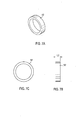
- show, respectively, a perspective view of the spring ring contact, and end view, a side view and an elevation view of the contact element.
- Fig. 6A, 6B and 6C
- show respectively a perspective view, a side view and an end view of a spacer usable in the present invention.
- Fig. 7A, 7B and 7C
- show, respectively, a perspective view, a side view and an end view of another spacer usable in the present invention.
- Fig. 8a, 8b and 8c
- show respectively a perspective, top plan view and an end view of the spacer bar of the invention
- Fig. 9
- shows a perspective view of an alternative embodiment of the spacer bar of the invention absent the contact elements.
- Fig. 10
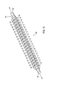
- shows a perspective view of an alternative embodiment of the spacer bar of the invention with contact elements mounted.
- Fig. 11A and 11B
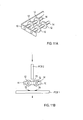
- show, respectively, partially fragmentary views of a connector frame and its use in a right angle connection.
- Referring now to Fig. 1, it should be seen that the array connector illustrated generally as 2 embodies the present invention.
- The
connector array 2 is comprised of aframe 10, which has a generally closed shape but can incorporate any geometric shape. In the illustrated embodiment the frame is shown as a square, but could take the form for example, of a rectangle or circle. As shown in Fig. 1, thearray connector 2 could be inserted between two spaced apartelectrical components connector 2. Conductive elements 7, 7' could be lands on a circuit substrate, solder masses on a BGA package or any other suitable arrangement. - As seen in Fig. 3 and 4, the
connector array 2 further includes a plurality ofcontact elements elongated spacer bar Contacts contact elements spacers contact elements contact elements contact plates 5,5'. Thecomponents 5, 5' engage opposite sides ofconnector 2. Any known clamping mechanism (not shown) can retaincomponents 5, 5' in suitable electrical connection withconnector 2. - As illustrated in Fig. 2A-2D, the
frame 10 has a plurality of alignedholes 20, 20' which are aligned with each other along opposite frame members so as to be able to receive one of the plurality of connectingrods spacer bar openings 20,20' to hold it in alignment within theframe 10 so that registration between thecontact elements connector 2 and the corresponding surface contacts 7,7 can be effected. - Referring for the moment to Fig. 8A-8C, it should be seen that each
spacer bar - Referring back to Fig. 3, 4, 5 and 6, the
spacer bar 14, one or more of thespacers conductive contacts elements assembly 25. As seen in Fig. 3, 4 and particularly in 5, eachcontact element 12 has a generally annular shape which is capable of compressing radially about thespacer bar 14. As best seen in Figures 5A-5C, the spacerbar contact elements interior opening 30 having a diameter D1 which can be somewhat greater in diameter than the outer diameter OD (see Fig. 4) of thespacer bar 14. Thespring contact elements - For example, in Fig. 3a and 3b, the contact element 12' has N° offset, yet has an interrupted
perimeter 19 making it radially yieldable. In the embodiment of Figures 3c and 3d, thecontact element 12" has a continuous annulus, yet is wider and has a thinner gauge thereby making it yieldable. In the embodiment of Figures 3e and 3f, thecontact element 12"' has apleat 23 formed in its perimeter thereby allowing it to be yieldable. In the embodiment of Figures 3e and 3f, thecontact element 12"" is a standard rigid washer and the diameter of its inner opening is such that the washer can tilt on thebar 14, e.g. yield, between fixedspacers bar 14 from an unloaded condition (Fig. 3g) to a loaded condition (Fig. 3h). - As best seen in Fig. 5A-5D, each
contact element spacer bar 14 is preferably smaller than the inner diameter D1 of theopening 30 of thecontact element 12, the lateral offset OF between theends contact plates 5,5' to be compressed radially about the corresponding one of the spacer bars 14,14 to which it is mounted to effect positive contact between one contact element 7 on oneplate 5 and the corresponding contact element 7 on the opposite plate 5'. - Referring now to the
spacer elements 16,16' used in the invention, and particularly as shown in Fig. 4 and in Fig. 6A-6C and 7A-7C, it should be seen that the spacer elements can take many different forms. Regardless of form, each spacer element is preferably made from an insulative material so as to electrically isolate adjacent contact elements from one another on the common spacer bar.Spacer 16 could be made, for example, from plastic or an elastomer. Since eachspacer bar contact element spacer bar 14 such that each is electrically isolated from theother contact elements 12 on the same bar. - Referring to Fig. 3 and 4, some
spacer elements 16,16' as shown in the embodiment of these figures, have alongitudinally extending slit 36 enabling it to be snap fitted overbar 14 and to be more versatile to adapt to varying and different diameters of the spacer bars and to accommodate manufacturing variation. However, it should be understood that it is wholly within the purview of the invention to provide spacer elements as shown in Figures 6 and 7 which have a complete and uninterrupted annulus, and thus have N° such longitudinal slot formed therein. - The spacers of Fig. 6 and 7 have lengths L1 and L2, respectively, which could be different. Such differing lengths allow almost infinite combinations of spacings to be made between
connector contact elements connector contact element 12 in registration with the corresponding pair (upper and lower ones of the conductive elements 7,7) on each of the oppositely disposedcomponents 5,5'. Thus, by varying combinations of thespacers 16 and 16' positioning of theconnector contact elements 12 can be infinitely effected. It should be further understood that each of thespacers 16,16' can be freely slidable along thespacer bar 14 about which it is disposed. - Each opposed pair of
openings frame 10 of thearray 2 slidably receives aspacer bar 14 therein. Eachspacer bar 14 has a length L which is longer than the width dimension W of theframe 10 defined between opposed inner side faces of theframe 10. In one method of assemblingconnector 2, eachspacer bar openings contact elements spacers 16,16' are inserted over the fed length of the spacer bar in accordance with the specifications of the job. Once this is complete, thespacer bar assembly 25 provides the ends of thespacer bar 14 with a small uncovered length. The uncovered length remains within the corresponding one of the openings pairs in the frame. Thereafter, the outer faces 40,40 of theframe 10 in which theopenings confines 13. Alternatively, retention structure, such as a cotter pin, could securerod 16 inframe 10 as a suitable retainer. In another alternative,frame 10 could be formed from several components that are built up aroundrods 16. - Referring now to Fig. 9 and 10, and to an alternative embodiment of the spacer bar assembly 25', it should be seen that the assembly illustrated includes a spacer bar referenced generally as 50 and is formed from an elastometic material, such as rubber. Each
such spacer bar 50 has integrally formed with it a plurality ofspacer bosses bar 50, these bosses are of an outer diameter which is slightly larger than the inner diameters D1 of thecontact elements contact elements bar 50 shown in this embodiment, thebosses contact element 12 disposed therebetween from unwanted axial movement within the gap between each boss. The assembly is fabricated by pulling the free ends 60,62 of the bar in the directions shown by the arrows to elongate it, and thereby reduce the outer diameter of the bosses. In so doing, one or more contact elements can be slid over the bosses until located in the designated gap defined by two consecutively spaced boss elements. Thereafter, the ends of the spacer bar can be released and the contact rims will be held in place thereon. - Fig. 11 displays an alternative arrangement of the present invention. Here, the
frame 10 is used as a connection between two perpendicularly oriented circuit boards, namely, board PCB1 and PCB2. That is, theframe 10 is located relative to boards PCB1 and PCB2 such that PCB2 is received withingap 70 disposed between opposed rows ofcontact elements - By the foregoing, an improved electrical connector for an array type contact scheme has been disclosed by way of the preferred invention. However, numerous modifications and substitutions may be had without departing from the spirit of the invention. For example, while the frame of the assembly has been shown in square shape, it is well within the purview of the invention to use any closed shape, preferably a parallelogram for mounting the spacer rods thereon.
- Accordingly, the invention has been described by way of illustration rather than limitation.
Claims (8)
- A method of manufacturing an electrical connector (2) for connecting conductive elements (7, 7') disposed on surfaces (9, 9') of two spaced apart electrical components (5, 5') comprising an array type contact grid characterized in that the array type contact grid comprises a plurality of contact elements (12, 12', 12") which can be readily varied in row position from row to row depending of the arrangement of said conductive elements (7, 7') onto the surfaces of said electrical components (5, 5').
- A method of assembling an electrical connector (2) according to claim 1 comprising:providing at least one spacer bar (14; 50) having a given outer diameter (OD);providing a plurality of contact elements (12, 12', 12") each having a hole formed therein defined generally by an inner diameter (D1) which is greater than the outer diameter (OD) of said spacer bar (14; 50);providing a plurality of spacer members(16, 16');placing a contact element (12, 12', 12") onto said bar (14) and spacing one contact element (12, 12', 12") from another on said bar (14) by placing one or more of said spacers (16, 16') there between.
- A method according to claim 2 characterized in that the assembly further comprises securing said at least one spacer bar (14) with said contact elements (12, 12', 12") and spacers (16, 16') thereon to a frame (10) to hold said at least one spacer bar (14) in place on said frame (10).
- A method according to claims 1 to 3 characterized in that each of said contact elements (12, 12', 12") is provided as a split ring capable of radially yielding inwardly.
- A method according to claim 2 characterized in that each of said spacers (16, 16') and said spacer bar (14) are provided as non-conductive members.
- A method according to claims 1 to 5 characterized in that the connector (2) is then inserted into a gap (70) between the two said spaced apart electrical components (5, 5') forming said gap (70) such that upon insertion of said connector (2) into said gap (70) the contact elements (12, 12', 12") are compressed.
- A method according to claim 2 characterized in that the spacer bar (14; 50) is made from an elastomeric material stretched such that the bar (14; 50) becomes elongated and of a reduced diameter so that a contact elements (12, 12', 12") can be placed on said stretched bar (14; 50).
- A method according to claim 7 characterized in that the said spacer bar (14; 50) is formed with a plurality of bosses (42, 42) with a gap between each boss into which gaps, a contact element (12, 12', 12") is placed.
Applications Claiming Priority (3)
| Application Number | Priority Date | Filing Date | Title |
|---|---|---|---|
| US42171699A | 1999-10-20 | 1999-10-20 | |
| US421716 | 1999-10-20 | ||
| EP20000122236 EP1094556B1 (en) | 1999-10-20 | 2000-10-17 | Low profile high density sockets |
Related Parent Applications (1)
| Application Number | Title | Priority Date | Filing Date |
|---|---|---|---|
| EP20000122236 Division EP1094556B1 (en) | 1999-10-20 | 2000-10-17 | Low profile high density sockets |
Publications (2)
| Publication Number | Publication Date |
|---|---|
| EP1315244A1 true EP1315244A1 (en) | 2003-05-28 |
| EP1315244B1 EP1315244B1 (en) | 2004-12-22 |
Family
ID=23671739
Family Applications (2)
| Application Number | Title | Priority Date | Filing Date |
|---|---|---|---|
| EP03001369A Expired - Lifetime EP1315244B1 (en) | 1999-10-20 | 2000-10-17 | Low profile high density sockets and related method of manufacturing |
| EP20000122236 Expired - Lifetime EP1094556B1 (en) | 1999-10-20 | 2000-10-17 | Low profile high density sockets |
Family Applications After (1)
| Application Number | Title | Priority Date | Filing Date |
|---|---|---|---|
| EP20000122236 Expired - Lifetime EP1094556B1 (en) | 1999-10-20 | 2000-10-17 | Low profile high density sockets |
Country Status (3)
| Country | Link |
|---|---|
| EP (2) | EP1315244B1 (en) |
| JP (1) | JP2001155804A (en) |
| DE (2) | DE60002412T2 (en) |
Cited By (2)
| Publication number | Priority date | Publication date | Assignee | Title |
|---|---|---|---|---|
| WO2005119848A1 (en) * | 2004-05-28 | 2005-12-15 | Molex Incorporated | Flexible ring interconnection system |
| WO2005119849A1 (en) * | 2004-05-28 | 2005-12-15 | Molex Incorporated | Flexible scrub ring contact |
Families Citing this family (1)
| Publication number | Priority date | Publication date | Assignee | Title |
|---|---|---|---|---|
| JP2006066407A (en) * | 2005-11-21 | 2006-03-09 | Micro Precision Kk | Silicon spring electrode and anisotropic conductive sheet |
Citations (5)
| Publication number | Priority date | Publication date | Assignee | Title |
|---|---|---|---|---|
| US5030109A (en) * | 1990-08-24 | 1991-07-09 | Amp Incorporated | Area array connector for substrates |
| US5061191A (en) * | 1990-12-21 | 1991-10-29 | Amp Incorporated | Canted coil spring interposing connector |
| US5232372A (en) * | 1992-05-11 | 1993-08-03 | Amp Incorporated | Land grid array connector and method of manufacture |
| US5273438A (en) * | 1992-08-19 | 1993-12-28 | The Whitaker Corporation | Canted coil spring array and method for producing the same |
| US5397240A (en) * | 1993-10-26 | 1995-03-14 | International Business Machines Corporation | Electrical connector |
Family Cites Families (4)
| Publication number | Priority date | Publication date | Assignee | Title |
|---|---|---|---|---|
| US3638163A (en) * | 1970-07-20 | 1972-01-25 | Bell Telephone Labor Inc | Connector for electrically interconnecting two parallel surfaces |
| GB1431185A (en) * | 1972-10-31 | 1976-04-07 | Int Computers Ltd | Electrical connectors and to methods for making electrical connec tors |
| US4142780A (en) * | 1974-03-29 | 1979-03-06 | Sharp Kabushiki Kaisha | Exchangeable liquid crystal panel |
| GB1536589A (en) * | 1976-05-15 | 1978-12-20 | Int Computers Ltd | Electrical connectors and to methods for making electrical connectors |
-
2000
- 2000-10-17 EP EP03001369A patent/EP1315244B1/en not_active Expired - Lifetime
- 2000-10-17 DE DE2000602412 patent/DE60002412T2/en not_active Expired - Fee Related
- 2000-10-17 EP EP20000122236 patent/EP1094556B1/en not_active Expired - Lifetime
- 2000-10-17 DE DE2000616982 patent/DE60016982T2/en not_active Expired - Fee Related
- 2000-10-20 JP JP2000321513A patent/JP2001155804A/en not_active Withdrawn
Patent Citations (5)
| Publication number | Priority date | Publication date | Assignee | Title |
|---|---|---|---|---|
| US5030109A (en) * | 1990-08-24 | 1991-07-09 | Amp Incorporated | Area array connector for substrates |
| US5061191A (en) * | 1990-12-21 | 1991-10-29 | Amp Incorporated | Canted coil spring interposing connector |
| US5232372A (en) * | 1992-05-11 | 1993-08-03 | Amp Incorporated | Land grid array connector and method of manufacture |
| US5273438A (en) * | 1992-08-19 | 1993-12-28 | The Whitaker Corporation | Canted coil spring array and method for producing the same |
| US5397240A (en) * | 1993-10-26 | 1995-03-14 | International Business Machines Corporation | Electrical connector |
Cited By (7)
| Publication number | Priority date | Publication date | Assignee | Title |
|---|---|---|---|---|
| WO2005119848A1 (en) * | 2004-05-28 | 2005-12-15 | Molex Incorporated | Flexible ring interconnection system |
| WO2005119849A1 (en) * | 2004-05-28 | 2005-12-15 | Molex Incorporated | Flexible scrub ring contact |
| US7189079B2 (en) | 2004-05-28 | 2007-03-13 | Molex Incorporated | Electro-formed ring interconnection system |
| US7229291B2 (en) | 2004-05-28 | 2007-06-12 | Molex Incorporated | Flexible ring interconnection system |
| US7273380B2 (en) | 2004-05-28 | 2007-09-25 | Molex Incorporated | Flexible ring interconnection system |
| US7284991B2 (en) | 2004-05-28 | 2007-10-23 | Molex Incorporated | Flexible scrub ring contact |
| KR100883455B1 (en) | 2004-05-28 | 2009-02-16 | 몰렉스 인코포레이티드 | Flexible rub ring contacts |
Also Published As
| Publication number | Publication date |
|---|---|
| EP1094556A2 (en) | 2001-04-25 |
| DE60002412D1 (en) | 2003-06-05 |
| EP1094556A3 (en) | 2001-10-24 |
| DE60016982D1 (en) | 2005-01-27 |
| DE60016982T2 (en) | 2005-12-29 |
| DE60002412T2 (en) | 2004-03-11 |
| EP1094556B1 (en) | 2003-05-02 |
| JP2001155804A (en) | 2001-06-08 |
| EP1315244B1 (en) | 2004-12-22 |
Similar Documents
| Publication | Publication Date | Title |
|---|---|---|
| US4593463A (en) | Method of making a contact assembly | |
| US8118604B2 (en) | Socket connector having electrical element supported by insulated elastomer | |
| US5366380A (en) | Spring biased tapered contact elements for electrical connectors and integrated circuit packages | |
| JP3885866B2 (en) | Connector assembly | |
| US8367942B2 (en) | Low profile electrical interposer of woven structure and method of making same | |
| US7572131B2 (en) | Electrical interconnect system utilizing non-conductive elastomeric elements | |
| US20050048807A1 (en) | Electrical contact and connector and method of manufacture | |
| US7833020B1 (en) | Electrical connector with low profile terminal | |
| CN101373866B (en) | Electrical connector with elastomeric element | |
| US7448877B1 (en) | High density flexible socket interconnect system | |
| CN101494330B (en) | Laminated electrical contact strip | |
| US7338294B2 (en) | Pressure contact connector | |
| JP4036376B2 (en) | connector | |
| US4943846A (en) | Pin grid array having seperate posts and socket contacts | |
| EP0437606A1 (en) | ELECTRIC CONNECTORS. | |
| EP1120870A2 (en) | Termination adapter for PCB | |
| US5540593A (en) | Coil type contactor and connector using the same | |
| US20040002234A1 (en) | Land grid array connector with canted electrical terminals | |
| US8172615B2 (en) | Electrical connector for an electronic module | |
| EP1094556B1 (en) | Low profile high density sockets | |
| TW202419878A (en) | Spring contact in a testing apparatus for integrated circuits | |
| NZ202553A (en) | Socket interfacing chip carrier with p.c.b. | |
| US6971885B2 (en) | Interconnect device with opposingly oriented contacts | |
| US7168958B1 (en) | Wadded-wire LGA contact with parallel solid conductor | |
| KR102331204B1 (en) | Electrical conducting device for electrical testing |
Legal Events
| Date | Code | Title | Description |
|---|---|---|---|
| PUAI | Public reference made under article 153(3) epc to a published international application that has entered the european phase |
Free format text: ORIGINAL CODE: 0009012 |
|
| AC | Divisional application: reference to earlier application |
Ref document number: 1094556 Country of ref document: EP Kind code of ref document: P |
|
| AK | Designated contracting states |
Designated state(s): DE FR GB IT |
|
| 17P | Request for examination filed |
Effective date: 20030929 |
|
| 17Q | First examination report despatched |
Effective date: 20031119 |
|
| AKX | Designation fees paid |
Designated state(s): DE FR GB IT |
|
| GRAP | Despatch of communication of intention to grant a patent |
Free format text: ORIGINAL CODE: EPIDOSNIGR1 |
|
| GRAS | Grant fee paid |
Free format text: ORIGINAL CODE: EPIDOSNIGR3 |
|
| GRAA | (expected) grant |
Free format text: ORIGINAL CODE: 0009210 |
|
| RAP1 | Party data changed (applicant data changed or rights of an application transferred) |
Owner name: FCI |
|
| AC | Divisional application: reference to earlier application |
Ref document number: 1094556 Country of ref document: EP Kind code of ref document: P |
|
| AK | Designated contracting states |
Kind code of ref document: B1 Designated state(s): DE FR GB IT |
|
| PG25 | Lapsed in a contracting state [announced via postgrant information from national office to epo] |
Ref country code: IT Free format text: LAPSE BECAUSE OF FAILURE TO SUBMIT A TRANSLATION OF THE DESCRIPTION OR TO PAY THE FEE WITHIN THE PRESCRIBED TIME-LIMIT;WARNING: LAPSES OF ITALIAN PATENTS WITH EFFECTIVE DATE BEFORE 2007 MAY HAVE OCCURRED AT ANY TIME BEFORE 2007. THE CORRECT EFFECTIVE DATE MAY BE DIFFERENT FROM THE ONE RECORDED. Effective date: 20041222 |
|
| REG | Reference to a national code |
Ref country code: GB Ref legal event code: FG4D |
|
| REF | Corresponds to: |
Ref document number: 60016982 Country of ref document: DE Date of ref document: 20050127 Kind code of ref document: P |
|
| ET | Fr: translation filed | ||
| PLBE | No opposition filed within time limit |
Free format text: ORIGINAL CODE: 0009261 |
|
| STAA | Information on the status of an ep patent application or granted ep patent |
Free format text: STATUS: NO OPPOSITION FILED WITHIN TIME LIMIT |
|
| 26N | No opposition filed |
Effective date: 20050923 |
|
| PGFP | Annual fee paid to national office [announced via postgrant information from national office to epo] |
Ref country code: GB Payment date: 20070918 Year of fee payment: 8 |
|
| PGFP | Annual fee paid to national office [announced via postgrant information from national office to epo] |
Ref country code: DE Payment date: 20071031 Year of fee payment: 8 |
|
| PGFP | Annual fee paid to national office [announced via postgrant information from national office to epo] |
Ref country code: FR Payment date: 20071004 Year of fee payment: 8 |
|
| GBPC | Gb: european patent ceased through non-payment of renewal fee |
Effective date: 20081017 |
|
| REG | Reference to a national code |
Ref country code: FR Ref legal event code: ST Effective date: 20090630 |
|
| PG25 | Lapsed in a contracting state [announced via postgrant information from national office to epo] |
Ref country code: DE Free format text: LAPSE BECAUSE OF NON-PAYMENT OF DUE FEES Effective date: 20090501 |
|
| PG25 | Lapsed in a contracting state [announced via postgrant information from national office to epo] |
Ref country code: FR Free format text: LAPSE BECAUSE OF NON-PAYMENT OF DUE FEES Effective date: 20081031 |
|
| PG25 | Lapsed in a contracting state [announced via postgrant information from national office to epo] |
Ref country code: GB Free format text: LAPSE BECAUSE OF NON-PAYMENT OF DUE FEES Effective date: 20081017 |