EP1315206A2 - Semiconductor apparatus of a plurality of semiconductor devices enclosed in a case and wiring method therefore - Google Patents
Semiconductor apparatus of a plurality of semiconductor devices enclosed in a case and wiring method therefore Download PDFInfo
- Publication number
- EP1315206A2 EP1315206A2 EP02026180A EP02026180A EP1315206A2 EP 1315206 A2 EP1315206 A2 EP 1315206A2 EP 02026180 A EP02026180 A EP 02026180A EP 02026180 A EP02026180 A EP 02026180A EP 1315206 A2 EP1315206 A2 EP 1315206A2
- Authority
- EP
- European Patent Office
- Prior art keywords
- wiring conductor
- case
- electrode wiring
- external connection
- connection terminal
- Prior art date
- Legal status (The legal status is an assumption and is not a legal conclusion. Google has not performed a legal analysis and makes no representation as to the accuracy of the status listed.)
- Withdrawn
Links
Images

Classifications
-
- H—ELECTRICITY
- H10—SEMICONDUCTOR DEVICES; ELECTRIC SOLID-STATE DEVICES NOT OTHERWISE PROVIDED FOR
- H10W—GENERIC PACKAGES, INTERCONNECTIONS, CONNECTORS OR OTHER CONSTRUCTIONAL DETAILS OF DEVICES COVERED BY CLASS H10
- H10W90/00—Package configurations
-
- H—ELECTRICITY
- H10—SEMICONDUCTOR DEVICES; ELECTRIC SOLID-STATE DEVICES NOT OTHERWISE PROVIDED FOR
- H10W—GENERIC PACKAGES, INTERCONNECTIONS, CONNECTORS OR OTHER CONSTRUCTIONAL DETAILS OF DEVICES COVERED BY CLASS H10
- H10W72/00—Interconnections or connectors in packages
- H10W72/50—Bond wires
- H10W72/531—Shapes of wire connectors
- H10W72/5363—Shapes of wire connectors the connected ends being wedge-shaped
-
- H—ELECTRICITY
- H10—SEMICONDUCTOR DEVICES; ELECTRIC SOLID-STATE DEVICES NOT OTHERWISE PROVIDED FOR
- H10W—GENERIC PACKAGES, INTERCONNECTIONS, CONNECTORS OR OTHER CONSTRUCTIONAL DETAILS OF DEVICES COVERED BY CLASS H10
- H10W72/00—Interconnections or connectors in packages
- H10W72/50—Bond wires
- H10W72/541—Dispositions of bond wires
- H10W72/547—Dispositions of multiple bond wires
- H10W72/5473—Dispositions of multiple bond wires multiple bond wires connected to a common bond pad
-
- H—ELECTRICITY
- H10—SEMICONDUCTOR DEVICES; ELECTRIC SOLID-STATE DEVICES NOT OTHERWISE PROVIDED FOR
- H10W—GENERIC PACKAGES, INTERCONNECTIONS, CONNECTORS OR OTHER CONSTRUCTIONAL DETAILS OF DEVICES COVERED BY CLASS H10
- H10W72/00—Interconnections or connectors in packages
- H10W72/50—Bond wires
- H10W72/541—Dispositions of bond wires
- H10W72/547—Dispositions of multiple bond wires
- H10W72/5475—Dispositions of multiple bond wires multiple bond wires connected to common bond pads at both ends of the wires
-
- H—ELECTRICITY
- H10—SEMICONDUCTOR DEVICES; ELECTRIC SOLID-STATE DEVICES NOT OTHERWISE PROVIDED FOR
- H10W—GENERIC PACKAGES, INTERCONNECTIONS, CONNECTORS OR OTHER CONSTRUCTIONAL DETAILS OF DEVICES COVERED BY CLASS H10
- H10W90/00—Package configurations
- H10W90/701—Package configurations characterised by the relative positions of pads or connectors relative to package parts
- H10W90/751—Package configurations characterised by the relative positions of pads or connectors relative to package parts of bond wires
- H10W90/753—Package configurations characterised by the relative positions of pads or connectors relative to package parts of bond wires between laterally-adjacent chips
-
- H—ELECTRICITY
- H10—SEMICONDUCTOR DEVICES; ELECTRIC SOLID-STATE DEVICES NOT OTHERWISE PROVIDED FOR
- H10W—GENERIC PACKAGES, INTERCONNECTIONS, CONNECTORS OR OTHER CONSTRUCTIONAL DETAILS OF DEVICES COVERED BY CLASS H10
- H10W90/00—Package configurations
- H10W90/701—Package configurations characterised by the relative positions of pads or connectors relative to package parts
- H10W90/751—Package configurations characterised by the relative positions of pads or connectors relative to package parts of bond wires
- H10W90/754—Package configurations characterised by the relative positions of pads or connectors relative to package parts of bond wires between a chip and a stacked insulating package substrate, interposer or RDL
Definitions
- the present invention relates to a semiconductor apparatus formed by enclosing a plurality of semiconductor devices in a case of resin, etc. and a wiring method for the semiconductor apparatus.
- a power module faces the task of reducing the circuit inductance in a power module using a switching element of a larger capacity and a higher switching frequency.
- Japanese Patent Publication No.2001-102519 suggests a power semiconductor module in which a first electrode pattern connected to a first electrode of the semiconductor device and a second electrode pattern connected to a second electrode of the semiconductor device are formed. With the configuration, a first electrode wiring conductor connected to the first electrode pattern and a second electrode wiring conductor connected to the second electrode pattern are provided above the second electrode pattern to successfully reduce the parasitic inductance of a circuit.
- FIG. 1 shows the internal structure of a semiconductor module 11 including a plurality of semiconductor devices 15.
- a wiring conductor for connection of an external connection terminal 13 to the source of the semiconductor device 15, and a wiring conductor for connection of an external connection terminal 14 to the drain of the semiconductor device 15 are inserted into a resin case 12.
- the external connection terminal 14 and the external connection terminal 13 are mounted on the separate sides so that they can be connected to the semiconductor device 15 through the bonding pads provided for the respective sides.
- the current path of the drain current cannot be set parallel to the current path of the source current. Therefore, it is difficult to reduce the parasitic inductance of a circuit.
- the object of the present invention is to reduce the parasitic inductance without increasing the number of assembly steps.
- the semiconductor apparatus is formed by enclosing a plurality of semiconductor devices in a case.
- each of the first and second wiring conductor through which a main current of the semiconductor device flows has an external connection terminal at one end, and being inserted into the case such that each wiring conductor can extend parallel to each other with the currents of the first and second wiring conductors flowing in the opposite directions.
- the first wiring conductor and the second wiring conductor extend in parallel, and the directions of their currents are opposite, thereby successfully reducing the parasitic inductance.
- the first external connection terminal of the first wiring conductor can be exposed to the outside of the resin case from the vicinity of the end portion of the first side of the frame of the resin case, and the second external connection terminal of the second wiring conductor can be exposed to the outside of the resin case from a side different from the first side of the frame.
- the first and second wiring conductors inserted into the resin case extend outside in parallel with the currents flowing in the opposite directions.
- the current entering through the first external connection terminal passes the first wiring conductor inserted into the resin case, and enters the first electrode of the semiconductor device. Further, it passes through the second electrode of the semiconductor device and the second wiring conductor extending parallel to the first wiring conductor, and exits from the second external connection terminal. Therefore, the flow of the current through the first wiring conductor is opposite in direction to the flow of the current through the second wiring conductor, thereby reducing the parasitic inductance of the first and second wiring conductors.
- the first connection unit of the first wiring conductor connected to the first electrode of the semiconductor device can be provided on the first side of the case, and the second connection unit of the second wiring conductor connected to the second electrode of the semiconductor device can be provided on a side different from the first side.
- the position of the wire bonding between the first electrode and the second electrode can be arbitrarily set, thereby enhancing the flexibility in arranging parts.
- the first external connection terminal can be provided on one side of the frame of the case, and the second external connection terminal can be mounted on a portion other than the frame of the case.
- the external connection terminal can be mounted in the position other than the frame of the case. Therefore, the flexibility in wiring an external circuit connected to the semiconductor apparatus can be increased.
- the surfaces on which the first wiring conductor and the second wiring conductor extend can be set parallel to the bottom of the case with the surfaces on which they extend can be set opposite to each other.
- the parasitic inductance by the first wiring conductor and the second wiring conductor can be further reduced.
- the surfaces on which the first wiring conductor and the second wiring conductor extend parallel to each other can be set perpendicular to the bottom of the case.
- the parasitic inductance of the semiconductor apparatus can be reduced, and the apparatus can be smaller.
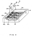
- FIG. 2 shows the internal structure of a power semiconductor module 21 according to the first embodiment of the present invention.
- the power semiconductor module (hereinafter referred to as a semiconductor module) 21 contains six semiconductor devices 23a through 23c comprising MOS transistors, and a drain electrode wiring conductor 24 connected to the drain electrodes of the semiconductor devices 23a through 23c and a source electrode wiring conductor 25 connected to the source electrodes are inserted into a case 22 of resin, etc.
- the drain electrodes and the source electrodes refer to the drain and source of the semiconductor devices 23a through 23c, or the connection areas for the wire bonding, or the connection area for wire bonding provided on the conductor layer directly connected to the semiconductor devices 23a through 23c, the conductor layer connected through wire, a metal plate, etc.
- the drain electrode wiring conductor 24 is inserted into one side 22a of the frame of the case 22, and one end extends (is exposed) from above the vicinity of the right end portion to the outside, and forms an external connection terminal 24a.
- the other end of the drain electrode wiring conductor 24 takes the form of a flat board, and extends along the side 22a of the frame of the case 22.
- the drain electrode wiring conductor 24 extending along the side 22a is exposed extending along the side 22a is exposed at the lower stage of the case 22, and forms a connection unit 24b.
- the connection unit 24b is connected to the substrate connected to the drain electrodes of the semiconductor devices 23a through 23c through the wire bonding.
- the source electrode wiring conductor 25 is inserted into the side 22a and a side 22c of the case 22, and its one end extends outside in the vicinity of the left end portion of the side 22c of the case 22, and forms an external connection terminal 25a.
- the other end of the source electrode wiring conductor 25 takes the form of a flat board, and extends parallel to the drain electrode wiring conductor 24. Furthermore, the source electrode wiring conductor 25 is exposed at the upper stage of the side 22a, and forms a connection unit 25b connected to the source electrodes of the semiconductor devices 23a through 23c.
- connection unit 24b of the drain electrode wiring conductor 24 formed at the lower stage of the case 22 is provided to the right of the connection unit 25b of the source electrode wiring conductor 25 at the upper stage, that is, closer to the semiconductor devices 23a through 23c. Therefore, when the wire bonding between the drain electrodes and the source electrodes of the semiconductor devices 23a through 23c is performed in the position where the wires overlap as viewed from above, the connection unit 24b at the lower stage can be first wire-bonded with the drain electrode, and then the connection unit 25b at the upper stage can be wire-bonded with the source electrode as connection over the first bonding wire, thereby preventing the lower wire from interfering with the upper wire bonding.
- the source electrode wiring conductor 25 at the upper stage of the case 22 is completely insulated from the unexposed portion of the drain electrode wiring conductor 24 at the lower stage by the case 22 of resin, etc.
- the current entering through the external connection terminal 24a passes the connection unit 24b extending along the lower stage of the case 22, and enters the drain electrodes of the semiconductor devices 23a through 23c after passing through a conductor layer 26 of the substrate.
- the current enters the drain electrodes it passes through the source electrodes of the semiconductor devices 23a through 23c, and then the connection unit 25b of the source electrode wiring conductor 25 extending parallel to the connection unit 24b of the drain electrode wiring conductor 24, and exits outside from the external connection terminal 25a.
- the current entering from the external connection terminal 24a of the drain electrode wiring conductor 24 enters the drain electrodes of the semiconductor devices 23a through 23c after flowing down as shown in FIG. 2 in the connection unit 24b of the drain electrode wiring conductor 24 extending parallel to the side 22a. Then, the current exiting the source electrodes of the semiconductor devices 23a through 23c flows upward as shown in FIG. 2 in the connection unit 25b of the source electrode wiring conductor 25, thereby exiting outside from the external connection terminal 25a.
- the drain electrode wiring conductor 24 and the source electrode wiring conductor 25 can be inserted into the case 22, the external connection terminal 24a of the drain electrode wiring conductor 24 is provided near the end portion of the side 22a, and the drain electrode wiring conductor 24 and the source electrode wiring conductor 25 are allowed to extend parallel to the side 22a of the case 22, thereby setting the flow of the current through the drain electrode wiring conductor 24 opposite in direction to the flow of the current through the source electrode wiring conductor 25.
- the parasitic inductance in the case 22 can be reduced.
- connection unit 24b at the lower stage is connected to the drain electrode, and the connection unit 25b at the upper stage is connected to the source electrode.
- connection unit at the lower stage can be connected to the source electrode, and the connection unit at the upper stage can be connected to the drain electrode.
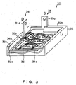
- FIG. 3 shows the internal structure of a semiconductor module 31 according to the second embodiment of the present invention.
- a drain electrode wiring conductor 34 is inserted into a side 32a of the frame of a case 32 and a side 32c on the near side, and the source electrode wiring conductor 35 is inserted into a side 32b and the side 32a of the frame of the case 32.
- One end of the drain electrode wiring conductor 34 extends upwards from above the right end of the side 32a of the case 32, and forms an external connection terminal 34a.
- the other end of the drain electrode wiring conductor 34 takes the form of a flat board, extends along the side 32a, forms an intermediate portion 34b, being bent by 90° at the corner made by the side 32a and the side 32c, extends along the side 32c, being exposed at the stage of the side 32c, and forms a connection unit 34c.
- the connection unit 34c is connected to the conductor layer 36 of the substrate connected to the drain electrodes of the semiconductor devices 23a through 23c through the wire.
- connection unit 34c of the drain electrode wiring conductor 34 is mounted on the side 32c opposing the side 32b for which an external connection terminal 35a of a source electrode wiring conductor 35 described later is provided.
- One end of the source electrode wiring conductor 35 extends upwards from above the substantially central portion of the side 32b of the case 32, and forms the external connection terminal 35a.
- the other end of the source electrode wiring conductor 35 takes the form of a flat board or a rectangular pillar, extends upwards above the intermediate portion 34b of the drain electrode wiring conductor 34, and forms the connection unit 35b connected to the source electrodes of the semiconductor devices 23a through 23c.
- the current entering from the external connection terminal 34a enters a conductor layer 36 from the connection unit 34c of the drain electrode wiring conductor 34 extending along the lower stage of the case 32.
- the current entering the conductor layer 36 further enters the drain electrodes of the semiconductor devices 23a through 23c, passes through the connection unit 35b of the source electrode wiring conductor 35 from the source electrodes of the semiconductor devices 23a through 23c, and exits from the external connection terminal 35a.
- the current entering from the external connection terminal 34a of the drain electrode flows through the intermediate portion 34b of the drain electrode wiring conductor 34 extending parallel to the side 32a downwards as shown in FIG. 3, and enters the drain electrodes of the semiconductor devices 23a through 23c from the curved connection unit 34c.
- the current which has entered the drain electrodes of the semiconductor devices 23a through 23c passes through the source electrode, flows through the connection unit 35b of the source electrode wiring conductor 35 extending parallel to the drain electrode wiring conductor 34 upwards as shown in FIG. 3, and exits from the external connection terminal 35a.
- the external connection terminal 34a of the drain electrode wiring conductor 34 extends outside from the vicinity of the right end of the side 32a of the case 32, the external connection terminal 35a of the source electrode wiring conductor 35 extends outside from the side 32b to the left of the side 32a, and the drain electrode wiring conductor 34 and the source electrode wiring conductor 35 extend parallel to each other.
- the current in the drain electrode wiring conductor 34 and the current in the source electrode wiring conductor 35 flow in the opposite directions in the side 32a.
- the parasitic inductance on the semiconductor module 31 can be reduced.
- connection unit 34c and the conductor layer 36 (connected to the drains of the semiconductor devices 23a through 23c) can be performed apart from the wire bonding between the connection unit 35b and the source electrodes of the semiconductor devices 23a through 23c by providing the connection unit 34c of the drain electrode wiring conductor 34 on the side 32c different from the side 32a on which the connection unit 35b of the source electrode wiring conductor 35 is provided, thereby reducing the restrictions on the bonding operation.
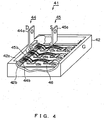
- FIG. 4 shows the internal structure of the semiconductor module according to the third embodiment of the present invention.
- the third embodiment is also configured by a drain electrode wiring conductor 44 and a source electrode wiring conductor 45 incorporated into a case 42.
- the drain electrode wiring conductor 44 is inserted into a side 42a of the frame of the case 42, and one end of the conductor extends outside from above the side 42a of the case 42, and forms an external connection terminal 44a.
- the other end of the drain electrode wiring conductor 44 takes the form of a flat board, extends along the side 42a, being exposed at the stage of the case 42, and forms a connection unit 44b.
- the connection unit 44b is connected through a wire, etc. to a conductor layer 46 of the substrate connected to the drain electrodes of the semiconductor devices 23a through 23c.
- the source electrode wiring conductor 45 is inserted into the side 42a of the frame of the case 42, and one end of the conductor extends parallel to the bottom of the case 42 in the direction perpendicular to the side 42a, thereby forming an external connection terminal 45a.
- the external connection terminal 45a is formed above perpendicular to the bottom when the wire bonding is performed, and is bent upward above the wire bonding portion after the wire bonding process. Therefore, the external connection terminal 45a does not actually interfere with the wire bonding operation.
- the other end of the source electrode wiring conductor 45 takes the form of a flat board or a rectangular pillar, extends above parallel to the drain electrode wiring conductor 44, and forms a connection unit 45b connected to the source electrodes of the semiconductor devices 23a through 23c.
- the third embodiment has the configuration in which the current entering from the external connection terminal 44a flows through the connection unit 44b of the drain electrode wiring conductor 44 downward as shown in FIG. 4, and enters the drain electrodes of the semiconductor devices 23a through 23c. Then the current exiting from the source electrodes of the semiconductor devices 23a through 23c flows upward as shown in FIG. 4, and exits from the external connection terminal 45a.
- the position of the external connection terminal 45a is not limited to the frame of the case 42. Therefore, the position of the external connection terminal 45a can be changed based on the arrangement of the connection unit of the external circuit. Furthermore, the semiconductor module 41 can be set smaller.
- the external connection terminal 45a of the source electrode wiring conductor 45 can be arranged on the side of the frame, and the external connection terminal 44a of the drain side can be arranged in the position other than the frame. Otherwise, when space can be reserved not to interfere the wire bonding, both external connection terminals can be arranged in the positions other than the frame of the case 42.
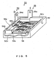
- FIG. 5 shows the internal structure of the semiconductor module according to the fourth embodiment of the present invention.
- the fourth embodiment is also configured by a drain electrode wiring conductor 54 and a source electrode wiring conductor 55 inserted and incorporated into a case 52.
- the drain electrode wiring conductor 54 is inserted into sides 52a and 52c of the frame of the case 52, and one end extends upward from above the vicinity of the right end portion of the side 52a, and forms the external connection terminal 54a.
- the other end of the drain electrode wiring conductor 54 extends along the sides 52a and 52c, takes the form of a board along the side 52a, and provided perpendicular to the bottom surface of the case 52. It also takes the form of the character L substantially in section along the side 52c, and the lower part of the L-shaped portion is exposed at the stage of the side 52c, thereby forming a connection unit 54c.
- the above mentioned connection unit 54c is connected through a wire, etc. to a conductor layer 56 of the substrate connected to the drain electrodes of the semiconductor devices 23a through 23c.
- the source electrode wiring conductor 55 is inserted into the sides 52a and 52b of the frame of the case 52, and one end extends upward right from the substantially central point of the side 52b, and forms an external connection terminal 55a.
- the other end of the source electrode wiring conductor 55 is substantially L-shaped in section, provided upward perpendicular to the bottom surface of the case 52, extends parallel to the drain electrode wiring conductor 54, being exposed at the stage, and forms a connection unit 55b.
- the connection unit 55b is connected to the source electrodes of the semiconductor devices 23a through 23c.
- the current flowing through a semiconductor module 51 according to the fourth embodiment is basically the same as that according to the above mentioned second embodiment.
- the current entering from an external connection terminal 54a of the drain electrode wiring conductor 54 enters the conductor layer 56 through the connection unit 54c of the drain electrode wiring conductor 54 extending along the sides 52a and 52c.
- the current entering the conductor layer 56 flows into the drain electrodes of the semiconductor devices 23a through 23c, passes through the connection unit 55b of the source electrode wiring conductor 55 extending along the side and the bottom of the case 52 from the semiconductor devices 23a through 23c, and exits from the external connection terminal 55a.
- the current flows downward as shown in FIG. 5 through the drain electrode wiring conductor 54 extending parallel to the side 52a, and the current (flowing upward as shown in FIG. 5) flows opposite in direction to the current flowing in the drain electrode wiring conductor 54.
- the magnetic fluxes generated by the current flowing through the drain electrode wiring conductor 54 and the current flowing through the source electrode wiring conductor 55 offset each other, thereby successfully reducing the parasitic inductance in the semiconductor module 51. Furthermore, the wire bonding between the drain electrode wiring conductor 54 and the conductor layer 56 and the wire bonding between the source electrode wiring conductor 55 and the semiconductor devices 23a through 23c, and the wire bonding between the source electrode wiring conductor 55 and the semiconductor devices 23a through 23c can be performed on the different sides in the case 52, thereby reducing the restriction conditions for the bonding operations.
- the surfaces of the drain electrode wiring conductor 54 and source electrode wiring conductor 55 facing each other are perpendicular to the bottom surface of the case 52, the ratio of area occupied by the drain electrode wiring conductor 54 and the source electrode wiring conductor 55 to the bottom area of the case 52 of the source electrode wiring conductor 55 can be reduced.
- the present invention is not limited to the above mentioned embodiment, but can also be configured as follows.
- the first wiring conductor and the second wiring conductor extend parallel to each other with their currents flowing in the opposite directions, thereby reducing the parasitic inductance by the first and second wiring conductors.
- the source electrode wiring conductor (25) also takes the form of a flat board, being inserted into the side (22a) and a side (22c), and extends parallel to a drain electrode wiring conductor (24) along the side (22a).
- the flow of the current in the drain electrode wiring conductor (24) is opposite in direction to the flow of the current in the source electrode wiring conductor (25).
Landscapes
- Inverter Devices (AREA)
- Wire Bonding (AREA)
- Insulated Gate Type Field-Effect Transistor (AREA)
Abstract
Description
Claims (8)
- A semiconductor apparatus formed by enclosing a plurality of semiconductor devices in a case, comprising a first wiring conductor (24) and a second wiring conductor (25), through which a main current of the semiconductor device (23a, 23b, 23c) flows, each wiring conductor (24, 25) having an external connection terminal (24a, 25a) at one end, and being inserted into the case such that each wiring conductor (24, 25) can extend parallel to each other with currents of the first and second wiring conductors (24, 25) flowing in opposite directions.
- The apparatus according to claim 1, wherein
a first external connection terminal (24a) of the first wiring conductor (24) can be exposed to outside of a resin case from a vicinity of an end portion of a first side of a frame of the resin case, and a second external connection terminal (25a) of the second wiring conductor (25) can be exposed to the outside of the resin case from a side different from the first side of the frame. - The apparatus according to claim 1, wherein
a first connection unit (24b) of the first wiring conductor (24) connected to a first electrode of the semiconductor device can be provided on a first side of the case, and a second connection unit (25b) of the second wiring conductor (25) connected to a second electrode of the semiconductor device can be provided on a side different from the first side. - The apparatus according to claim 1, wherein
the first external connection terminal (24a) can be provided on one side of the frame of the case, and the second external connection terminal (25a) can be mounted on a portion other than the frame of the case. - The apparatus according to claim 1, wherein
surfaces on which the first wiring conductor (24) and the second wiring conductor (25) extend in parallel can be set parallel to a bottom of the case with surfaces on which the conductors (24, 25) extend can be set opposite to each other. - The apparatus according to claim 1, wherein
surfaces on which the first wiring conductor (24) and the second wiring conductor (25) extend in parallel can be set perpendicular to the bottom of the case. - A wiring method for a semiconductor apparatus formed by enclosing a plurality of semiconductor devices in a case, wherein
a main current of the semiconductor device (23a , 23b , 23c) flows through a first wiring conductor (24) and a second wiring conductor (25), each wiring conductor (24, 25) having an external connection terminal (24a, 25a) at one end, and being inserted into the case such that each wiring conductor (24 , 25) can extend parallel to each other with currents of the first and second wiring conductors (24, 25) flowing in opposite directions; and
the first wiring conductor (24) is connected to a first electrode of the semiconductor device (23a, 23b, 23c) , and the second wiring conductor (25) is connected to a second electrode of the semiconductor device (23a, 23b, 23c). - The method according to claim 7, wherein
a first external connection terminal (24a) can be exposed to outside of a resin case from a vicinity of an end portion of a first side of the resin case, and a second external connection terminal (25a) can be exposed to the outside of the resin case from a side different from the first side of the frame.
Applications Claiming Priority (2)
| Application Number | Priority Date | Filing Date | Title |
|---|---|---|---|
| JP2001359156A JP4066644B2 (en) | 2001-11-26 | 2001-11-26 | Semiconductor device and wiring method of semiconductor device |
| JP2001359156 | 2001-11-26 |
Publications (2)
| Publication Number | Publication Date |
|---|---|
| EP1315206A2 true EP1315206A2 (en) | 2003-05-28 |
| EP1315206A3 EP1315206A3 (en) | 2006-03-29 |
Family
ID=19170213
Family Applications (1)
| Application Number | Title | Priority Date | Filing Date |
|---|---|---|---|
| EP20020026180 Withdrawn EP1315206A3 (en) | 2001-11-26 | 2002-11-25 | Semiconductor apparatus of a plurality of semiconductor devices enclosed in a case and wiring method therefore |
Country Status (3)
| Country | Link |
|---|---|
| US (1) | US7161235B2 (en) |
| EP (1) | EP1315206A3 (en) |
| JP (1) | JP4066644B2 (en) |
Families Citing this family (8)
| Publication number | Priority date | Publication date | Assignee | Title |
|---|---|---|---|---|
| JP4363190B2 (en) * | 2004-01-08 | 2009-11-11 | 株式会社豊田自動織機 | Semiconductor device and manufacturing method thereof |
| US8018056B2 (en) * | 2005-12-21 | 2011-09-13 | International Rectifier Corporation | Package for high power density devices |
| JP4242401B2 (en) * | 2006-06-29 | 2009-03-25 | 三菱電機株式会社 | Semiconductor device |
| JP5601376B2 (en) * | 2010-12-01 | 2014-10-08 | 株式会社安川電機 | Power converter |
| US8405206B1 (en) * | 2011-09-30 | 2013-03-26 | Infineon Technologies Ag | Low-inductive semiconductor module |
| JP6725004B2 (en) * | 2016-11-11 | 2020-07-15 | 三菱電機株式会社 | Semiconductor device, inverter unit and automobile |
| JP6352556B1 (en) * | 2017-06-19 | 2018-07-04 | 新電元工業株式会社 | Semiconductor device |
| CN112582369A (en) * | 2020-12-15 | 2021-03-30 | 华芯威半导体科技(北京)有限责任公司 | Lead terminal and power module using same |
Family Cites Families (22)
| Publication number | Priority date | Publication date | Assignee | Title |
|---|---|---|---|---|
| JPS61139051A (en) * | 1984-12-11 | 1986-06-26 | Toshiba Corp | Semiconductor device |
| DE8700978U1 (en) | 1987-01-21 | 1987-03-05 | Siemens AG, 1000 Berlin und 8000 München | Semiconductor arrangement with at least one semiconductor body |
| JP3053298B2 (en) | 1992-08-19 | 2000-06-19 | 株式会社東芝 | Semiconductor device |
| US5523620A (en) * | 1994-02-14 | 1996-06-04 | Delco Electronics Corporation | Coplanar linear dual switch module |
| KR0148077B1 (en) * | 1994-08-16 | 1998-08-01 | 김광호 | Semiconductor Package With Separate Die Pads |
| JP3269745B2 (en) * | 1995-01-17 | 2002-04-02 | 株式会社日立製作所 | Modular semiconductor device |
| JP3357220B2 (en) * | 1995-07-07 | 2002-12-16 | 三菱電機株式会社 | Semiconductor device |
| JP3480771B2 (en) * | 1995-12-20 | 2003-12-22 | 三菱電機株式会社 | Semiconductor device |
| JPH1022451A (en) * | 1996-07-01 | 1998-01-23 | Mitsubishi Electric Corp | Semiconductor device |
| JP3013794B2 (en) * | 1996-12-10 | 2000-02-28 | 富士電機株式会社 | Semiconductor device |
| JPH1168035A (en) * | 1997-06-12 | 1999-03-09 | Hitachi Ltd | Power semiconductor module |
| US6138349A (en) * | 1997-12-18 | 2000-10-31 | Vlt Corporation | Protective coating for an electronic device |
| TW473882B (en) * | 1998-07-06 | 2002-01-21 | Hitachi Ltd | Semiconductor device |
| JP3521757B2 (en) | 1998-09-08 | 2004-04-19 | 株式会社豊田自動織機 | Semiconductor module electrode structure |
| JP3519300B2 (en) * | 1999-01-11 | 2004-04-12 | 富士電機デバイステクノロジー株式会社 | Power module package structure |
| JP2000216331A (en) * | 1999-01-25 | 2000-08-04 | Mitsubishi Electric Corp | Power semiconductor module and power conversion device using the same |
| JP3798184B2 (en) * | 1999-06-09 | 2006-07-19 | 矢崎総業株式会社 | Power semiconductor module |
| US6242707B1 (en) * | 1999-08-31 | 2001-06-05 | General Electric Company | Arc quenching current limiting device including ablative material |
| JP4292652B2 (en) | 1999-09-30 | 2009-07-08 | 三菱電機株式会社 | Power semiconductor module |
| JP3695260B2 (en) | 1999-11-04 | 2005-09-14 | 株式会社日立製作所 | Semiconductor module |
| JP3633432B2 (en) * | 2000-03-30 | 2005-03-30 | 株式会社日立製作所 | Semiconductor device and power conversion device |
| JP3692906B2 (en) * | 2000-05-25 | 2005-09-07 | 日産自動車株式会社 | Power wiring structure and semiconductor device |
-
2001
- 2001-11-26 JP JP2001359156A patent/JP4066644B2/en not_active Expired - Fee Related
-
2002
- 2002-11-21 US US10/301,252 patent/US7161235B2/en not_active Expired - Fee Related
- 2002-11-25 EP EP20020026180 patent/EP1315206A3/en not_active Withdrawn
Also Published As
| Publication number | Publication date |
|---|---|
| JP2003158231A (en) | 2003-05-30 |
| US7161235B2 (en) | 2007-01-09 |
| US20030100148A1 (en) | 2003-05-29 |
| JP4066644B2 (en) | 2008-03-26 |
| EP1315206A3 (en) | 2006-03-29 |
Similar Documents
| Publication | Publication Date | Title |
|---|---|---|
| KR101194609B1 (en) | Power semiconductor module | |
| US9236321B2 (en) | Semiconductor device and manufacturing method thereof | |
| US8810013B2 (en) | Integrated power converter package with die stacking | |
| US6465875B2 (en) | Semiconductor device package with plural pad lead frame | |
| US7592688B2 (en) | Semiconductor package | |
| US12469826B2 (en) | Semiconductor module | |
| US20130258628A1 (en) | Power converter | |
| KR102499825B1 (en) | Packaged power semiconductor device | |
| KR20090064334A (en) | Semiconductor devices | |
| KR20150140600A (en) | Power semiconductor device | |
| JP2020098811A (en) | Semiconductor device and electric power conversion apparatus | |
| EP0987762B1 (en) | Semiconductor module | |
| US7821128B2 (en) | Power semiconductor device having lines within a housing | |
| KR101231792B1 (en) | Semiconductor package | |
| US7161235B2 (en) | Semiconductor apparatus of a plurality of semiconductor devices enclosed in case and wiring method therefore | |
| US20020158327A1 (en) | Semiconductor device | |
| CN114300435A (en) | Semiconductor module | |
| US6664629B2 (en) | Semiconductor device | |
| JP7392308B2 (en) | semiconductor equipment | |
| JP4246040B2 (en) | Semiconductor device package | |
| EP0527033A2 (en) | Semiconductor module | |
| JP3906710B2 (en) | Semiconductor device and manufacturing method thereof | |
| JP3906433B2 (en) | Semiconductor device and wiring method of semiconductor device | |
| US11508698B2 (en) | Semiconductor package and semiconductor device | |
| US20260026406A1 (en) | Semiconductor arrangement |
Legal Events
| Date | Code | Title | Description |
|---|---|---|---|
| PUAI | Public reference made under article 153(3) epc to a published international application that has entered the european phase |
Free format text: ORIGINAL CODE: 0009012 |
|
| 17P | Request for examination filed |
Effective date: 20021125 |
|
| AK | Designated contracting states |
Designated state(s): AT BE BG CH CY CZ DE DK EE ES FI FR GB GR IE IT LI LU MC NL PT SE SK TR |
|
| AX | Request for extension of the european patent |
Extension state: AL LT LV MK RO SI |
|
| PUAL | Search report despatched |
Free format text: ORIGINAL CODE: 0009013 |
|
| AK | Designated contracting states |
Kind code of ref document: A3 Designated state(s): AT BE BG CH CY CZ DE DK EE ES FI FR GB GR IE IT LI LU MC NL PT SE SK TR |
|
| AX | Request for extension of the european patent |
Extension state: AL LT LV MK RO SI |
|
| AKX | Designation fees paid |
Designated state(s): AT BE BG CH CY CZ DE DK EE ES FI FR GB GR IE IT LI LU MC NL PT SE SK TR |
|
| STAA | Information on the status of an ep patent application or granted ep patent |
Free format text: STATUS: THE APPLICATION IS DEEMED TO BE WITHDRAWN |
|
| 18D | Application deemed to be withdrawn |
Effective date: 20080602 |