EP1315203A2 - Semiconductor device with different bonding configurations - Google Patents
Semiconductor device with different bonding configurations Download PDFInfo
- Publication number
- EP1315203A2 EP1315203A2 EP02025499A EP02025499A EP1315203A2 EP 1315203 A2 EP1315203 A2 EP 1315203A2 EP 02025499 A EP02025499 A EP 02025499A EP 02025499 A EP02025499 A EP 02025499A EP 1315203 A2 EP1315203 A2 EP 1315203A2
- Authority
- EP
- European Patent Office
- Prior art keywords
- leads
- electrode pads
- lead
- semiconductor chip
- semiconductor device
- Prior art date
- Legal status (The legal status is an assumption and is not a legal conclusion. Google has not performed a legal analysis and makes no representation as to the accuracy of the status listed.)
- Withdrawn
Links
Images




Classifications
-
- H—ELECTRICITY
- H10—SEMICONDUCTOR DEVICES; ELECTRIC SOLID-STATE DEVICES NOT OTHERWISE PROVIDED FOR
- H10D—INORGANIC ELECTRIC SEMICONDUCTOR DEVICES
- H10D84/00—Integrated devices formed in or on semiconductor substrates that comprise only semiconducting layers, e.g. on Si wafers or on GaAs-on-Si wafers
- H10D84/01—Manufacture or treatment
-
- H—ELECTRICITY
- H10—SEMICONDUCTOR DEVICES; ELECTRIC SOLID-STATE DEVICES NOT OTHERWISE PROVIDED FOR
- H10W—GENERIC PACKAGES, INTERCONNECTIONS, CONNECTORS OR OTHER CONSTRUCTIONAL DETAILS OF DEVICES COVERED BY CLASS H10
- H10W72/00—Interconnections or connectors in packages
-
- H—ELECTRICITY
- H10—SEMICONDUCTOR DEVICES; ELECTRIC SOLID-STATE DEVICES NOT OTHERWISE PROVIDED FOR
- H10D—INORGANIC ELECTRIC SEMICONDUCTOR DEVICES
- H10D86/00—Integrated devices formed in or on insulating or conducting substrates, e.g. formed in silicon-on-insulator [SOI] substrates or on stainless steel or glass substrates
- H10D86/01—Manufacture or treatment
-
- H—ELECTRICITY
- H10—SEMICONDUCTOR DEVICES; ELECTRIC SOLID-STATE DEVICES NOT OTHERWISE PROVIDED FOR
- H10W—GENERIC PACKAGES, INTERCONNECTIONS, CONNECTORS OR OTHER CONSTRUCTIONAL DETAILS OF DEVICES COVERED BY CLASS H10
- H10W70/00—Package substrates; Interposers; Redistribution layers [RDL]
- H10W70/40—Leadframes
- H10W70/481—Leadframes for devices being provided for in groups H10D8/00 - H10D48/00
-
- H—ELECTRICITY
- H10—SEMICONDUCTOR DEVICES; ELECTRIC SOLID-STATE DEVICES NOT OTHERWISE PROVIDED FOR
- H10W—GENERIC PACKAGES, INTERCONNECTIONS, CONNECTORS OR OTHER CONSTRUCTIONAL DETAILS OF DEVICES COVERED BY CLASS H10
- H10W70/00—Package substrates; Interposers; Redistribution layers [RDL]
- H10W70/60—Insulating or insulated package substrates; Interposers; Redistribution layers
- H10W70/62—Insulating or insulated package substrates; Interposers; Redistribution layers characterised by their interconnections
- H10W70/65—Shapes or dispositions of interconnections
- H10W70/658—Shapes or dispositions of interconnections for devices provided for in groups H10D8/00 - H10D48/00
-
- H—ELECTRICITY
- H10—SEMICONDUCTOR DEVICES; ELECTRIC SOLID-STATE DEVICES NOT OTHERWISE PROVIDED FOR
- H10W—GENERIC PACKAGES, INTERCONNECTIONS, CONNECTORS OR OTHER CONSTRUCTIONAL DETAILS OF DEVICES COVERED BY CLASS H10
- H10W70/00—Package substrates; Interposers; Redistribution layers [RDL]
- H10W70/60—Insulating or insulated package substrates; Interposers; Redistribution layers
- H10W70/62—Insulating or insulated package substrates; Interposers; Redistribution layers characterised by their interconnections
- H10W70/65—Shapes or dispositions of interconnections
- H10W70/654—Top-view layouts
- H10W70/656—Fan-in layouts
-
- H—ELECTRICITY
- H10—SEMICONDUCTOR DEVICES; ELECTRIC SOLID-STATE DEVICES NOT OTHERWISE PROVIDED FOR
- H10W—GENERIC PACKAGES, INTERCONNECTIONS, CONNECTORS OR OTHER CONSTRUCTIONAL DETAILS OF DEVICES COVERED BY CLASS H10
- H10W72/00—Interconnections or connectors in packages
- H10W72/01—Manufacture or treatment
- H10W72/0198—Manufacture or treatment batch processes
-
- H—ELECTRICITY
- H10—SEMICONDUCTOR DEVICES; ELECTRIC SOLID-STATE DEVICES NOT OTHERWISE PROVIDED FOR
- H10W—GENERIC PACKAGES, INTERCONNECTIONS, CONNECTORS OR OTHER CONSTRUCTIONAL DETAILS OF DEVICES COVERED BY CLASS H10
- H10W72/00—Interconnections or connectors in packages
- H10W72/071—Connecting or disconnecting
- H10W72/073—Connecting or disconnecting of die-attach connectors
- H10W72/07351—Connecting or disconnecting of die-attach connectors characterised by changes in properties of the die-attach connectors during connecting
- H10W72/07353—Connecting or disconnecting of die-attach connectors characterised by changes in properties of the die-attach connectors during connecting changes in shapes
-
- H—ELECTRICITY
- H10—SEMICONDUCTOR DEVICES; ELECTRIC SOLID-STATE DEVICES NOT OTHERWISE PROVIDED FOR
- H10W—GENERIC PACKAGES, INTERCONNECTIONS, CONNECTORS OR OTHER CONSTRUCTIONAL DETAILS OF DEVICES COVERED BY CLASS H10
- H10W72/00—Interconnections or connectors in packages
- H10W72/30—Die-attach connectors
- H10W72/331—Shapes of die-attach connectors
- H10W72/334—Cross-sectional shape, i.e. in side view
-
- H—ELECTRICITY
- H10—SEMICONDUCTOR DEVICES; ELECTRIC SOLID-STATE DEVICES NOT OTHERWISE PROVIDED FOR
- H10W—GENERIC PACKAGES, INTERCONNECTIONS, CONNECTORS OR OTHER CONSTRUCTIONAL DETAILS OF DEVICES COVERED BY CLASS H10
- H10W72/00—Interconnections or connectors in packages
- H10W72/50—Bond wires
- H10W72/531—Shapes of wire connectors
- H10W72/536—Shapes of wire connectors the connected ends being ball-shaped
-
- H—ELECTRICITY
- H10—SEMICONDUCTOR DEVICES; ELECTRIC SOLID-STATE DEVICES NOT OTHERWISE PROVIDED FOR
- H10W—GENERIC PACKAGES, INTERCONNECTIONS, CONNECTORS OR OTHER CONSTRUCTIONAL DETAILS OF DEVICES COVERED BY CLASS H10
- H10W72/00—Interconnections or connectors in packages
- H10W72/50—Bond wires
- H10W72/541—Dispositions of bond wires
- H10W72/5449—Dispositions of bond wires not being orthogonal to a side surface of the chip, e.g. fan-out arrangements
-
- H—ELECTRICITY
- H10—SEMICONDUCTOR DEVICES; ELECTRIC SOLID-STATE DEVICES NOT OTHERWISE PROVIDED FOR
- H10W—GENERIC PACKAGES, INTERCONNECTIONS, CONNECTORS OR OTHER CONSTRUCTIONAL DETAILS OF DEVICES COVERED BY CLASS H10
- H10W72/00—Interconnections or connectors in packages
- H10W72/851—Dispositions of multiple connectors or interconnections
- H10W72/874—On different surfaces
- H10W72/884—Die-attach connectors and bond wires
-
- H—ELECTRICITY
- H10—SEMICONDUCTOR DEVICES; ELECTRIC SOLID-STATE DEVICES NOT OTHERWISE PROVIDED FOR
- H10W—GENERIC PACKAGES, INTERCONNECTIONS, CONNECTORS OR OTHER CONSTRUCTIONAL DETAILS OF DEVICES COVERED BY CLASS H10
- H10W72/00—Interconnections or connectors in packages
- H10W72/90—Bond pads, in general
- H10W72/931—Shapes of bond pads
-
- H—ELECTRICITY
- H10—SEMICONDUCTOR DEVICES; ELECTRIC SOLID-STATE DEVICES NOT OTHERWISE PROVIDED FOR
- H10W—GENERIC PACKAGES, INTERCONNECTIONS, CONNECTORS OR OTHER CONSTRUCTIONAL DETAILS OF DEVICES COVERED BY CLASS H10
- H10W72/00—Interconnections or connectors in packages
- H10W72/90—Bond pads, in general
- H10W72/931—Shapes of bond pads
- H10W72/932—Plan-view shape, i.e. in top view
-
- H—ELECTRICITY
- H10—SEMICONDUCTOR DEVICES; ELECTRIC SOLID-STATE DEVICES NOT OTHERWISE PROVIDED FOR
- H10W—GENERIC PACKAGES, INTERCONNECTIONS, CONNECTORS OR OTHER CONSTRUCTIONAL DETAILS OF DEVICES COVERED BY CLASS H10
- H10W74/00—Encapsulations, e.g. protective coatings
-
- H—ELECTRICITY
- H10—SEMICONDUCTOR DEVICES; ELECTRIC SOLID-STATE DEVICES NOT OTHERWISE PROVIDED FOR
- H10W—GENERIC PACKAGES, INTERCONNECTIONS, CONNECTORS OR OTHER CONSTRUCTIONAL DETAILS OF DEVICES COVERED BY CLASS H10
- H10W90/00—Package configurations
- H10W90/701—Package configurations characterised by the relative positions of pads or connectors relative to package parts
- H10W90/731—Package configurations characterised by the relative positions of pads or connectors relative to package parts of die-attach connectors
- H10W90/734—Package configurations characterised by the relative positions of pads or connectors relative to package parts of die-attach connectors between a chip and a stacked insulating package substrate, interposer or RDL
-
- H—ELECTRICITY
- H10—SEMICONDUCTOR DEVICES; ELECTRIC SOLID-STATE DEVICES NOT OTHERWISE PROVIDED FOR
- H10W—GENERIC PACKAGES, INTERCONNECTIONS, CONNECTORS OR OTHER CONSTRUCTIONAL DETAILS OF DEVICES COVERED BY CLASS H10
- H10W90/00—Package configurations
- H10W90/701—Package configurations characterised by the relative positions of pads or connectors relative to package parts
- H10W90/731—Package configurations characterised by the relative positions of pads or connectors relative to package parts of die-attach connectors
- H10W90/736—Package configurations characterised by the relative positions of pads or connectors relative to package parts of die-attach connectors between a chip and a stacked lead frame, conducting package substrate or heat sink
-
- H—ELECTRICITY
- H10—SEMICONDUCTOR DEVICES; ELECTRIC SOLID-STATE DEVICES NOT OTHERWISE PROVIDED FOR
- H10W—GENERIC PACKAGES, INTERCONNECTIONS, CONNECTORS OR OTHER CONSTRUCTIONAL DETAILS OF DEVICES COVERED BY CLASS H10
- H10W90/00—Package configurations
- H10W90/701—Package configurations characterised by the relative positions of pads or connectors relative to package parts
- H10W90/751—Package configurations characterised by the relative positions of pads or connectors relative to package parts of bond wires
- H10W90/754—Package configurations characterised by the relative positions of pads or connectors relative to package parts of bond wires between a chip and a stacked insulating package substrate, interposer or RDL
-
- H—ELECTRICITY
- H10—SEMICONDUCTOR DEVICES; ELECTRIC SOLID-STATE DEVICES NOT OTHERWISE PROVIDED FOR
- H10W—GENERIC PACKAGES, INTERCONNECTIONS, CONNECTORS OR OTHER CONSTRUCTIONAL DETAILS OF DEVICES COVERED BY CLASS H10
- H10W90/00—Package configurations
- H10W90/701—Package configurations characterised by the relative positions of pads or connectors relative to package parts
- H10W90/751—Package configurations characterised by the relative positions of pads or connectors relative to package parts of bond wires
- H10W90/756—Package configurations characterised by the relative positions of pads or connectors relative to package parts of bond wires between a chip and a stacked lead frame, conducting package substrate or heat sink
Definitions
- This invention relates to a semiconductor device and its packaging, specifically to a packaging of a semiconductor switching device that accommodates a change in an input scheme of control signals of the switching device by changing wire bonding positions while using a same semiconductor chip and a same lead pattern.
- Switching elements for high frequency signals have been a focus of development in many application areas including mobile communication equipment that utilizes microwaves in GHz frequency range and alternates antennas and receiving/transmitting signals.
- Such a device is described, for example, in a Japanese Laid Open Patent Publication, No. Hei 9-181642.
- This type of device often includes a field effect transistor (FET) functioning as a high frequency switch, which is made of gallium arsenide (GaAs), and is integrated as a monolithic microwave integrated circuit (MMIC) having the high frequency switches.
- FET field effect transistor
- FIG. 1A is a plan view of a conventional packaging of a semiconductor switching device 63
- FIG. 1B is a schematic cross-sectional view of the packaging of FIG. 1A cut along line B-B.
- the chip 63 is made of a gallium arsenide (GaAs), and has an electrode pad I for an input signal, two electrode pads C1, C2 for a pair of control signals and two electrode pads O1, 02 for an output signal.
- the input electrode pad I is located between the two input electrode pads C1, C2.
- the chip 63 is mounted on an island 62e using a conducting paste 70, such as a solder.
- the electrode pads on the top surface of the chip 63 are connected to respective leads of a lead pattern 62 by bonding wires 64.
- the control electrode pad C1 is connected to a lead 62a
- the input electrode pad I is connected to a lead 62b
- the control electrode pad C2 is connected to a lead 62c
- the two output electrode pads 01, 02 are connected to leads 62d, 62f, respectively.
- the island 62e of the lead pattern 62 which is electrically connected to the chip 63, is connected a ground voltage (reference voltage).
- a resin body 75 covers the chip 63 and the central portion of the lead pattern 62. The far ends of the leads extrude from the side of the resin body 75.
- the lead pattern 62 is formed by a conventional stamping process.
- the semiconductor switching device 63 has two switches (not shown in the figure), and each switch receives a control signal through the corresponding control electrode pad C1, C2, i.e., C1 is for a first switch and C2 is for a second switch, respectively.
- a switch is typically made of a field effect transistor (FET).
- a pair of control signals for example signals A and B (not shown in the figure), which complement each other, is inputted to the two control electrode pads C1, C2, and then applied to the two switches of the device through the control electrode pads C1, C2.
- signal A is applied to the first switch of the device through the control electrode pad C1
- signal B is applied to the second switch of the device through the control electrode pad C2.
- the chip 63 is manufactured to meet this specification so that the two control electrode pads C1, C2 are located close to the corresponding switches, respectively.
- This design is referred to as a normal control switch, and schematically shown in FIG. 2.
- signal A be applied to the second switch and signal B be applied to the first switch.
- This is referred to as a reverse control switch, and schematically shown in FIG. 3.
- additional wiring is required to reverse the signal inputs as shown in FIG. 3. Accordingly, two different device manufacturing processes must be established for the two different device designs. This complicates the manufacturing processes.
- the invention provides a semiconductor device including an insulating substrate, a plurality of leads disposed on the substrate, and a semiconductor chip mounted on the insulating substrate and having a plurality of electrode pads disposed on its surface.
- the electrodes pads are connected to the respective leads.
- the semiconductor chip is disposed with respect to two of the leads to leave areas of each of the two leads not covered by semiconductor chip at both ends of the semiconductor chip.
- the areas of the two leads are large enough for connecting corresponding leads to the corresponding electrode pads.
- a first of the two leads is connected to a first of the two electrode pads and a second of the two leads is connected to a second of the two electrode pads when the devise is configured so that first of the two electrode pads receives a first signal and the second of the two electrode pads receives a second signal.
- the first of the two leads is connected to the second of the two electrode pads and the second of the two leads is connected to the first of the two electrode pads when the device is configured so that the first of the two electrode pads receives the second signal and the second of the two electrode pads receives the first signal.
- the invention also provides a semiconductor device including a resin body, a plurality of leads embedded in the resin body, and a semiconductor chip embedded in the resin body and having a plurality of electrode pads disposed on its surface.
- the electrodes pads are connected to the respective leads.
- the semiconductor chip is disposed with respect to two of the leads to leave areas of each of the two leads not covered by the semiconductor chip at both ends of the semiconductor chip. The areas of the two leads are large enough for connecting the two leads to the corresponding electrode pads.
- a first of the two leads is connected to a first of the two electrode pads and a second of the two leads is connected to a second of the electrode pads when the semiconductor device is configured so that the first of the two electrode pads receives a first signal and the second of the two electrode pads receives a second signal.
- the first of the two leads is connected to the second of the two electrode pads and the second of the two leads is connected to the first of the two electrode pads when the semiconductor device is configured so that the first of the two electrode pads receives the second signal and the second of the two electrode pads receives the first signal.
- the invention further provides a device packaging including an insulating substrate, a first lead disposed on the insulating substrate, a second lead disposed on the insulating substrate, and a surface mounting element mounted on the first and second leads so that each of the leads is left not covered by the surface mounting element at both ends of the surface mounting element.
- the invention also provides a device packaging including a resin body, a first lead embedded in the resin body, a second lead embedded in the resin body, and a surface mounting element mounted on the first and second leads so that each of the leads is left not covered by the surface mounting element at both ends of the surface mounting element.
- the invention further provides a method of fabricating devices with different internal wiring.
- This method includes providing lead wiring means for allowing alternative wire bonding configurations, which has a first lead and a second lead, and mounting a surface mounting element on the lead wiring means, which has a first electrode pad and a second electrode pad.
- the method also includes connecting the first electrode pad to the first lead by a first bonding wire and connecting the second electrode pad to the second lead by a second bonding wire so that the first and second bonding wires do not intersect each other when a device of a first wiring configuration is fabricated, and connecting the first electrode pad to the second lead by the first bonding wire and connecting the second electrode pad to the first lead by the second bonding wire so that the first and second bonding wires do not intersect each other when a device of a second wiring configuration is fabricated.
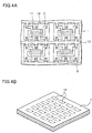
- FIG. 4A is a plan view of a lead pattern 2 formed on an insulating substrate 1 of the first embodiment.
- the insulating substrate 1 is a large insulating plate made of a ceramic, a glass epoxy resin or the like, or a stack of such a insulating plate.
- the total thickness of the insulating substrate 1 is 180 to 250 ⁇ m so that the substrate can withstand mechanical stresses it receives during manufacturing processes.
- the lead pattern 2 for one packaging area 10 which is indicated by an unevenly broken line, includes six individual leads that are formed on the insulating substrate 1 and correspond to electrode pads formed on a semiconductor chip for packaging.
- the semiconductor chip is mounted on a chip mounting area 11.
- the six leads are formed by a gold plating, and two of the six leads penetrate through the chip mounting area 11 to provide areas for wire bonding at both ends of the chip mounting area 11.
- the lead pattern 2 does not have an island, such as the one shown FIG. 1A, and a semiconductor chip is mounted on the two leads penetrating though the chip mounting area 11 using an insulating resin. All the lead patterns 2 are identical among the individual packaging areas 10, and connected by a connection portion 12.
- the packaging area 10 is about 1.2 mm x 0.8 mm, and the chip mounting area 11 is about 0.30 mm x 0.37 mm, although the size of the chip mounting area 11 should be adjusted according to the size of a chip mounted thereon.
- the separation between the package areas 10 are about 100 ⁇ m in both longitudinal and the transverse directions. This separation is required for dicing the substrate 1 to separate individual completed packaging.
- the connection portion 12 is required to form the lead pattern 2 using gold plating. When electroless plating is used for forming the lead pattern 2, the connection portion is not required and the package areas 10 are formed to be separated from each other.
- FIG. 4B is a perspective view of the insulating substrate 1 used in the first embodiment.
- the substrate 1 is large enough to provide more than one hundred package areas 10.
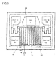
- FIG. 5 is a plan view of the semiconductor chip 3 used in the first embodiment.
- the semiconductor chip 3 is a compound semiconductor switching device, and its circuit elements are formed on a GaAs substrate.
- the backside of the GaAs substrate is semi-insulating.
- the chip has two FETs, FET1, FET2 positioned in the central portion of the GaAs substrate.
- the gate electrodes 17 of FET1 and FET2 are connected to control electrode pads C1, C2, respectively, through corresponding resistors R1, R2.
- Both of the drain electrodes 15 of the two FETs are connected to an input electrode pad I.
- the source electrodes 13 of the two FETs are connected to output electrode pads 01, 02, respectively.
- a gate metal layer 20 made of Ti/Pt/Au is a second wiring layer indicated by the dotted lines in the figure, and includes the gate electrode 17, which forms a Schottky contact with a channel region of each FET.
- a pad metal layer 40 made of Ti/Pt/Au is a third wiring layer indicated by the solid lines in the figure, and provides electrode pads and connection between circuit elements.
- An ohmic metal layer made of AuGe/Ni/Au is a first wiring layer, and forms a ohmic contact with the GaAs substrate. The ohmic metal layer provides the source electrodes 13 and the drain electrodes 15 of the two FETs as well as contact portions of the resistors. The ohmic metal layer overlaps with the pad metal layer 40 and is omitted in the figure.
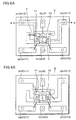
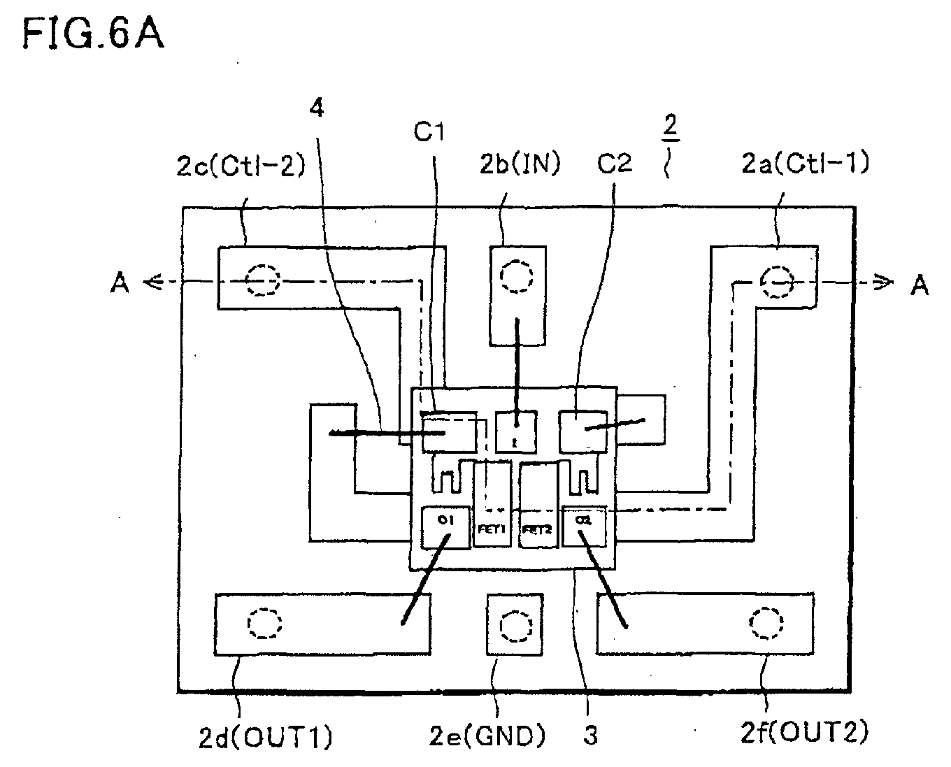
- FIGS. 6A and 6B show two different configurations of the packaging of the first embodiment, which utilize the same lead pattern of FIG. 4A and the same semiconductor chip of FIG. 5.
- the semiconductor chip 3 is mounted on the two leads 2a, 2c penetrating through the chip mounting area using an insulating resin adhesive.
- the two leads 2a, 2c run underneath the semiconductor chip 3, and provides areas not covered by the semiconductor chip 3 at both ends of the semiconductor chip 3, that are large enough for connecting leads to the corresponding electrode pads on the semiconductor chip 3 by wire bonding.
- the mounting position of the semiconductor chip 3 may be adjusted as long as the uncovered areas are large enough and close enough to the chip 3 for wire bonding.
- a lead 2b is connected to the input electrode pad I, a lead 2d to the output electrode pad O1, a lead 2f to the output electrode pad 02, the lead 2c to the control electrode pad C2, and the lead 2a to the control electrode pad C1. All the connections are made by wire-bonding the leads to the corresponding electrode pads by ball bonding or wedge bonding.
- the control electrode pad C1 may be connected to either of the two penetrating leads 2a, 2c at the left end of the semiconductor chip 3. In this configuration, it is connected to the lead 2a.
- the control electrode pad C2 is connected to the lead 2c, instead of the lead 2a, at the right end of the semiconductor chip 3.
- the lead 2e is at a ground voltage (reference voltage).
- the configuration of FIG. 6B is a normal control switch and the configuration of FIG. 6A is a reverse control switch.
- signal A of the pair is applied to the lead 2c and signal B of the pair is applied to the lead 2a.
- signal A is applied to the gate electrode 17 of the FEF1 through the electrode pad C1
- signal B is applied to the gate electrode 17 of the FET2 through the electrode pad C2.
- signal A is applied to the gate electrode 17 of FET2 and signal B is applied to the gate electrode 17 of the FET1.
- the same lead pattern of FIG. 4A and the same semiconductor chip of FIG. 5 are used.
- the only difference is the connections between the penetrating leads 2a, 2c and the corresponding electrode pads C1, C2. These connections are made just by connecting the leads 2a, 2c to the corresponding electrode pads C1, C2.
- the packaging of the first embodiment provides both the normal and reverse control switches without any modification to the chip or the lead pattern.
- the lead pattern 2 is formed by a plating process based on thick film printing. Accordingly, the separations between the leads are as small as 75 ⁇ m. This contributes to reduction of overall packaging size because the minimum separation of the conventional lead pattern formed by stamping of FIG. 1A is as large as 120 ⁇ m, which is decided by 0.8 x frame thickness (150 ⁇ m).
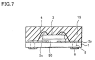
- FIG. 7 is a schematic cross-sectional view of the packaging structure of FIG. 6A cut along line A-A.
- the compound semiconductor chip 3 is mounted on the leads 2a, 2c with an insulating resin adhesive 50.
- the electrode pads are connected to the corresponding leads by the bonding wires 4.
- a through hole 5 is formed in the insulating substrate 1 for each of the leads, and connect the lead to a corresponding external electrode 6 formed on the backside of the insulating substrate 1.
- the through holes are filled with conducting materials such as tungsten.
- a resin body 15 seals the semiconductor chip 3.
- six external electrodes 6 are positioned near the edge of the insulating substrate 1 in a symmetrical manner. Namely, the external electrodes 6 for the electrode pads C1, I, C2 are lined up along the top edge of insulating substrate 1, and the external electrodes 6 for the electrode pads O1, 02 and the ground lead 2e are lined up along the bottom edge of the insulating substrate 1.
- top and bottom surfaces of the individual packaging are a flattened top surface of the resin body 15 and the bottom surface of the insulating substrate 1, respectively.
- the thickness of the resin body is about 0.3 mm and the thickness of the semiconductor chip 3 is about 130 ⁇ m.
- an identification marking for each external electrode 6 is formed on the top surface of the resin layer 15 at a corresponding location. Marking may be formed by indenting the top surface or printing the top surface.
- lead pattern 2 is formed on the insulating substrate 1 by gold plating or the like in this embodiment, overall packaging size is much smaller than the size of the conventional packaging of FIG. 1A, in which a lead pattern is made by stamping a metal plate.
- FIG. 8A is a cross-sectional view of the semiconductor device of the second embodiment.
- the lead pattern of this embodiment is substantially the same as the lead pattern 2 of the first embodiment as shown in FIG. 4A.
- the packaging structure of this embodiment is similar to the packaging structure of the first embodiment shown in the plan view of FIGS. 6A and 6B.
- the cross section of FIG. 8A is made along line A-A of FIG. 6A. All the leads and the corresponding electrode pads on the chip are positioned and connected in the same manner as in the two configurations of the first embodiment.
- the chip 23 used in this embodiment is the same chip used in the first embodiment.
- This packaging also provides two different switches, a normal control switch and a reverse control switch, using the same lead pattern and the same chip just by changing the wire bond connection of two leads.
- the difference between the two embodiments is that the lead pattern 22 of the second embodiment is embedded in and supported by the resin body 21. No other support is provided in the second embodiment for the lead pattern 22 of the device.
- the lead pattern 2 of the first embodiment is supported by the insulating substrate 1.
- the resin layer 21 covers the lead pattern 22 and the chip 23, and fills the space 31 between portions of the lead pattern 22.
- the chip 23 is mounted on the leads 22a, 22c (2a 2c in FIG. 6A) with an insulating adhesive 50.
- the side of the lead pattern 22 is curved inwardly (not shown in the figure) for engaging with the resin body 21 to strengthen the connection between the resin body 21 and the lead pattern 22.
- a thermosetting resin such as an epoxy resin
- a thermoplastic resin such as a polyimide resin and a polyphenylene sulfide resin, is used to form the resin body 21 by injection molding.
- the thickness of the resin body 21 is adjusted so that the separation between the top of the bonding wire 24 and the top surface of the resin body 21 is about 50 ⁇ m. The thickness may vary depending on the mechanical strength required for the packaging.
- the packaging structure is annealed to flatten out the top surface of the resin body 21. This annealing is required to suppress the bending of the packaging due to the difference in thermal expansion coefficients between the lead pattern 22 and the resin body 21 as well as the difference in contraction rate after a re-flow process.
- FIG. 8B is a cross-sectional view of a device intermediate to form the device shown in FIG. 8A.
- the lead pattern 22 is formed by creating the space 31 in a conductive foil 30. At this point of manufacturing step, all the lead patterns are a part of the continuous conductive foil 30, as shown in FIG. 9B. Removing the backside of the conductive foil 30 separates the conductive foil 30 into individual lead patterns. The removing methods include grinding, polishing, etching and laser evaporation among other methods. As a result, the lead pattern 22 is exposed on the backside of the resin body 21, and the back surface of the lead pattern 22 and the back surface of the resin body 21 are at the same level.
- a photoresist layer 27 covers the back side of the packaging and has openings to expose the backside of the leads. Solder bumps are formed in the openings to work as external electrodes 26. These solder bumps are movable under surface tension during the mounting of the device on a circuit board so that the device and the board are aligned by itself.
- FIG. 9A is a plan view of a conductive foil 30 used for forming the packaging structure of the second embodiment.
- the conductive foil 30 is made of copper, and its thickness before the removal of the backside is about 70 ⁇ m. The thickness may be anywhere between 10 and 300 ⁇ m, and can be outside this range provided that the depth of the space 31 is shorter than the thickness of the conductive foil 30.
- a plurality of frames 32 is formed in the conductive foil 30.
- the conductive foil 30 may be also made of aluminium or an iron-nickel alloy. If requirements for adhesion to the soldering materials, adhesion to the resin layer and plating of other metal are met, other metals can be used as the conductive foil 30.
- FIG. 9B is an expanded plan view of one frame 32 of the conductive foil 30 of FIG. 9A.
- the frame 32 contains 25 package areas 10, one of which is indicated by the area encircled by the dotted line in the figure.
- the portions encircled by the solid lines represent the portions of the conductive foil 30 that are not etched, and the other portions of the package area 10 represent the portions of the conductive foil 30 that are etched to form the space 31.
- the unetched portions provide the lead pattern 22 after the backside of the conductive foil 30 is removed. Because the lead pattern 22 is formed by etching, the separations between the leads can be as small as the spatial resolution of the etching method. This contributes to reduction of overall packaging size.
- the conductive foil 30 supports the chip 23 until the resin body 21 covers the chip 23 and the lead pattern 22. This removes the requirement of an additional support, i.e., the insulating substrate 1 of the first embodiment. Because of the absence of the rigid substrate, the flexible sheet like structure of the conductive foil 30 makes handling of the device intermediate easy and simple during the manufacturing.
- FIG. 10 is a plan view of the packaging of the first embodiment with an alternative lead configuration.
- This lead configuration is the same as the lead configuration of FIG. 6A except that the leads 2a, 2c do not run underneath the semiconductor chip and instead run along the edge of the chip.
- each of the two leads 2a, 2c has areas enough for wire bonding at both ends of the semiconductor chip.
- the packaging of the first embodiment with this alternative lead configuration also provides both the normal and reverse control switches without any modification to the chip or the lead pattern.
- This alternative lead configuration is also applied to the second embodiment. It should noted that in the embodiments described above the boding wires are configured not to intersect each other.
- a switching device made of a compound semiconductor is mounted on the lead pattern.
- other semiconductor chips including other integrated circuits, transistors and diodes that are made of silicon or compound semiconductor, can be mounted on the lead pattern in the packaging.
- passive elements including chip capacitors, chip resistors and chip inductors, can be also mounted.
- Elements that are mounted with the top surface facing the lead pattern can be also mounted in this packaging structure. In other words, any surface mounting element can be used in the packaging of this invention.
Landscapes
- Wire Bonding (AREA)
- Semiconductor Integrated Circuits (AREA)
- Lead Frames For Integrated Circuits (AREA)
Abstract
Description
Claims (19)
- A semiconductor device comprising:wherein the semiconductor chip (3) is disposed with respect to two of the leads (2a, 2c) to leave areas of each of the two leads not covered by semiconductor chip (3) at both ends of the semiconductor chip (3), the areas of the two leads (2a, 2c) being large enough for connecting the two leads to the corresponding electrode pads (C1, C2), andan insulating substrate (1);a plurality of leads (2) disposed on the substrate (1); anda semiconductor chip (3) mounted on the insulating substrate (1) and having a plurality of electrode pads (I, C1, C2, O1, 02) disposed on a surface thereof, the electrodes pads (I, C1, C2, O1, 02) being connected to the leads respectively,
a first (2a) of the two leads is connected to a first (C1) of the two electrode pads and a second (2c) of the two leads is connected to a second (C2) of the two electrode pads when the semiconductor device is configured so that the first (C1) of the two electrode pads receives a first signal and the second (C2) of the two electrode pads receives a second signal, and the first (2a) of the two leads is connected to the second (C2) of the two electrode pads and the second (2c) of the two leads is connected to the first (C1) of the two electrode pads when the semiconductor device is configured so that the first (C1) of the two electrode pads receives the second signal and the second (C2) of the two electrode pads receives the first signal. - The semiconductor device of claim 1, wherein the semiconductor chip (3) comprises a compound semiconductor chip having a bottom portion (50) that is semi-insulating and faces the insulating substrate (1).
- The semiconductor device of claim 1, wherein the semiconductor chip (3) is mounted on the two leads (2a, 2c) using an insulating resin.
- The semiconductor device according to any of claims 1 to 3, further comprising a plurality of bonding wires (4) connecting the leads (2) to the corresponding electrode pads (I, C1, C2, O1, 02), wherein connections between the two leads (2a, 2c) and the corresponding two electrode pads (C1, C2) are alternated by bonding the corresponding bonding wires (4) at the areas of the two leads (2a, 2c) at the different ends of the semiconductor chip (3).
- The semiconductor device according to any of claims 1 to 4, wherein the semiconductor chip (3) comprises a switching circuit, and the two electrode pads (C1, C2) receive control signals of the switching circuit.
- The semiconductor device according to any of claims 1 to 5, further comprising a plurality of through holes (5) penetrating through the insulating substrate (1), each of the through holes (5) being connected to one of the leads (2), and a plurality of external electrodes (6) formed on a backside of the insulating substrate (1), each of external electrodes (6) being connected to one of the through holes (5).
- A semiconductor device comprising:wherein the semiconductor chip (23) is disposed with respect to two of the leads (22a, 22c) to leave areas of each of the two leads (22a, 22c) not covered by the semiconductor chip (23) at both ends of the semiconductor chip, the areas of the two leads (22a, 22c) being large enough for connecting the two leads to the corresponding electrode pads (C1, C2), and a first of the two leads (22a) is connected to a first of the two electrode pads (C1) and a second of the two leads (22c) is connected to a second (C2) of the two electrode pads when the semiconductor device is configured so that the first (C1) of the two electrode pads receives a first signal and the second (C2) of the two electrode pads receives a second signal, and the first (22a) of the two leads is connected to the second (C2) of the two electrode pads and the second (22c) of the two leads is connected to the first (C1) of the two electrode pads when the semiconductor device is configured so that the first (C1) of the two electrode pads receives the second signal and the second (C2) of the two electrode pads receives the first signal.a resin body (21);a plurality of leads (22) embedded in the resin body (21); anda semiconductor chip (23) embedded in the resin body (21) and having a plurality of electrode pads (I, C1, C2, O1, 02) disposed on a surface thereof, the electrodes pads (I, C1, C2, O1, 02) being connected to the leads (22) respectively,
- The semiconductor device of claim 7, wherein the semiconductor chip (23) comprises a compound semiconductor chip having a bottom portion (50) that is semi-insulating and faces the leads (22).
- The semiconductor device of claim 7, wherein the semiconductor chip is mounted on the two leads using an insulating resin (21).
- The semiconductor device according to any of claims 7 to 9, further comprising a plurality of bonding wires (24) connecting the leads (22) to the corresponding electrode pads, wherein connections between the two leads and the corresponding two electrode pads are alternated by bonding the corresponding bonding wires (24) at the areas of the two leads at the different ends of the semiconductor chip (23).
- The semiconductor device according to any of claims 7 to 10, wherein the semiconductor chip comprises a switching circuit, and the two electrode pads receive control signals of the switching circuit.
- The semiconductor device according to any of claims 7 to 11, further comprising a plurality of external electrodes (26) formed on backsides of the leads (22).
- A device packaging comprising:an insulating substrate (1);a first lead (2a) disposed on the insulating substrate;a second lead (2c) disposed on the insulating substrate; anda surface mounting element (3) mounted on the first and second leads (2a, 2c) so that each of the leads (2a, 2c) is not covered by the surface mounting element (3) at both ends of the surface mounting element (3).
- A device packaging comprising:a resin body (21);a first lead embedded in the resin body (21);a second lead embedded in the resin body (21); anda surface mounting element (23) mounted on the first and second leads so that each of the leads is not covered by the surface mounting element (23) at both ends of the surface mounting element (23).
- A method of fabricating devices with different internal wiring configurations, the method comprising:providing lead wiring means (2) for allowing alternative wire bonding configurations, the lead wiring means comprising a first lead (2a) and a second lead (2c);mounting a surface mounting element (3) on the lead wiring means (2), the surface mounting element (3) comprising a first electrode pad (C1) and a second electrode pad (C2); andconnecting the first electrode pad (C1) to the first lead (2a) by a first bonding wire and connecting the second electrode pad (C2) to the second lead (2c) by a second bonding wire so that the first and second bonding wires do not intersect each other, when a device of a first wiring configuration is fabricated, andconnecting the first electrode pad (C1) to the second lead (2c) by the first bonding wire and connecting the second electrode pad (C2) to the first lead (2a) by the second bonding wire so that the first and second bonding wires do not intersect each other, when a device of a second wiring configuration is fabricated.
- The method of fabricating devices with different internal wiring configurations of claim 15, further comprising forming the lead wiring means (2) on an insulating substrate (1).
- The method of fabricating devices with different internal wiring of claim 16, further comprising providing an external electrode (6) for each of the leads (2) on a backside of the insulating substrate (1), each of the external electrodes (6) being connected to the corresponding lead (2) by a corresponding through hole (5) formed in the insulating substrate (1).
- The method of fabricating devices with different internal wiring configurations of claim 15, further comprising covering the lead wiring means (2) and the surface mounting element (3) with a resin (15).
- The method of fabricating devices with different internal wiring configurations of claim 18, further comprising removing a backside of the lead wiring means (2).
Applications Claiming Priority (2)
| Application Number | Priority Date | Filing Date | Title |
|---|---|---|---|
| JP2001350553A JP3920629B2 (en) | 2001-11-15 | 2001-11-15 | Semiconductor device |
| JP2001350553 | 2001-11-15 |
Publications (2)
| Publication Number | Publication Date |
|---|---|
| EP1315203A2 true EP1315203A2 (en) | 2003-05-28 |
| EP1315203A3 EP1315203A3 (en) | 2006-04-05 |
Family
ID=19163027
Family Applications (1)
| Application Number | Title | Priority Date | Filing Date |
|---|---|---|---|
| EP20020025499 Withdrawn EP1315203A3 (en) | 2001-11-15 | 2002-11-15 | Semiconductor device with different bonding configurations |
Country Status (6)
| Country | Link |
|---|---|
| US (1) | US6833608B2 (en) |
| EP (1) | EP1315203A3 (en) |
| JP (1) | JP3920629B2 (en) |
| KR (1) | KR100679185B1 (en) |
| CN (1) | CN1282241C (en) |
| TW (1) | TW561599B (en) |
Families Citing this family (7)
| Publication number | Priority date | Publication date | Assignee | Title |
|---|---|---|---|---|
| JP4765004B2 (en) | 2006-09-04 | 2011-09-07 | 富士電機株式会社 | Semiconductor device and manufacturing method thereof |
| US8072065B2 (en) * | 2008-02-14 | 2011-12-06 | Viasat, Inc. | System and method for integrated waveguide packaging |
| US8592960B2 (en) | 2010-08-31 | 2013-11-26 | Viasat, Inc. | Leadframe package with integrated partial waveguide interface |
| JP5809500B2 (en) | 2011-09-16 | 2015-11-11 | ルネサスエレクトロニクス株式会社 | Semiconductor device |
| CN103928431B (en) * | 2012-10-31 | 2017-03-01 | 矽力杰半导体技术(杭州)有限公司 | A kind of flip-chip packaged device |
| CN110892522B (en) * | 2017-08-01 | 2023-09-12 | 株式会社村田制作所 | High frequency switch |
| US20210376563A1 (en) * | 2020-05-26 | 2021-12-02 | Excelitas Canada, Inc. | Semiconductor Side Emitting Laser Leadframe Package and Method of Producing Same |
Family Cites Families (16)
| Publication number | Priority date | Publication date | Assignee | Title |
|---|---|---|---|---|
| US4595945A (en) * | 1983-10-21 | 1986-06-17 | At&T Bell Laboratories | Plastic package with lead frame crossunder |
| EP0162521A3 (en) * | 1984-05-23 | 1986-10-08 | American Microsystems, Incorporated | Package for semiconductor devices |
| US4612564A (en) * | 1984-06-04 | 1986-09-16 | At&T Bell Laboratories | Plastic integrated circuit package |
| US4937656A (en) * | 1988-04-22 | 1990-06-26 | Mitsubishi Denki Kabushiki Kaisha | Semiconductor device |
| US5976912A (en) * | 1994-03-18 | 1999-11-02 | Hitachi Chemical Company, Ltd. | Fabrication process of semiconductor package and semiconductor package |
| JPH08148603A (en) * | 1994-11-22 | 1996-06-07 | Nec Kyushu Ltd | Ball grid array type semiconductor device and method of manufacturing the same |
| US6066890A (en) * | 1995-11-13 | 2000-05-23 | Siliconix Incorporated | Separate circuit devices in an intra-package configuration and assembly techniques |
| US5691568A (en) * | 1996-05-31 | 1997-11-25 | Lsi Logic Corporation | Wire bondable package design with maxium electrical performance and minimum number of layers |
| US5825628A (en) * | 1996-10-03 | 1998-10-20 | International Business Machines Corporation | Electronic package with enhanced pad design |
| US5907769A (en) * | 1996-12-30 | 1999-05-25 | Micron Technology, Inc. | Leads under chip in conventional IC package |
| US6103547A (en) * | 1997-01-17 | 2000-08-15 | Micron Technology, Inc. | High speed IC package configuration |
| US6054754A (en) * | 1997-06-06 | 2000-04-25 | Micron Technology, Inc. | Multi-capacitance lead frame decoupling device |
| JP2954110B2 (en) * | 1997-09-26 | 1999-09-27 | 九州日本電気株式会社 | CSP type semiconductor device and manufacturing method thereof |
| JP4037589B2 (en) * | 2000-03-07 | 2008-01-23 | 三菱電機株式会社 | Resin-encapsulated power semiconductor device |
| TW530455B (en) * | 2001-04-19 | 2003-05-01 | Sanyo Electric Co | Switch circuit device of compound semiconductor |
| JP2003204009A (en) * | 2001-11-01 | 2003-07-18 | Sanyo Electric Co Ltd | Semiconductor device |
-
2001
- 2001-11-15 JP JP2001350553A patent/JP3920629B2/en not_active Expired - Fee Related
-
2002
- 2002-10-11 TW TW91123400A patent/TW561599B/en not_active IP Right Cessation
- 2002-11-13 KR KR20020070315A patent/KR100679185B1/en not_active Expired - Fee Related
- 2002-11-15 US US10/294,912 patent/US6833608B2/en not_active Expired - Lifetime
- 2002-11-15 CN CNB021506507A patent/CN1282241C/en not_active Expired - Fee Related
- 2002-11-15 EP EP20020025499 patent/EP1315203A3/en not_active Withdrawn
Also Published As
| Publication number | Publication date |
|---|---|
| KR20030040128A (en) | 2003-05-22 |
| CN1420559A (en) | 2003-05-28 |
| TW561599B (en) | 2003-11-11 |
| US20030137044A1 (en) | 2003-07-24 |
| EP1315203A3 (en) | 2006-04-05 |
| US6833608B2 (en) | 2004-12-21 |
| JP3920629B2 (en) | 2007-05-30 |
| JP2003152009A (en) | 2003-05-23 |
| KR100679185B1 (en) | 2007-02-07 |
| CN1282241C (en) | 2006-10-25 |
Similar Documents
| Publication | Publication Date | Title |
|---|---|---|
| KR100599364B1 (en) | Compound semiconductor switch curcuit device | |
| US4647959A (en) | Integrated circuit package, and method of forming an integrated circuit package | |
| KR101037997B1 (en) | A semiconductor die package and a substrate for a semiconductor die package, a method of forming the same, and a manufacturing method and processing method of a lead frame structure | |
| US6921980B2 (en) | Integrated semiconductor circuit including electronic component connected between different component connection portions | |
| EP0500690B1 (en) | Multi-layer lead frames for integrated circuit packages | |
| US7348663B1 (en) | Integrated circuit package and method for fabricating same | |
| HK1008115B (en) | Multi-layer lead frames for integrated circuit packages | |
| US7723161B2 (en) | Lead frame, method of manufacturing the same, semiconductor device using lead frame and method of manufacturing semiconductor device | |
| US5426319A (en) | High-frequency semiconductor device including microstrip transmission line | |
| US6818969B2 (en) | Semiconductor device | |
| US6833616B2 (en) | Multilayer wiring board with mounting pad | |
| US12622279B2 (en) | Package with dual layer routing including ground return path | |
| US6833608B2 (en) | Semiconductor device and packaging system therefore | |
| KR20230051585A (en) | semiconductor device | |
| KR20080026221A (en) | Semiconductor device manufacturing method, device chip packaging method, semiconductor device and array | |
| US20080123299A1 (en) | Circuit Device and Manufacturing Method of the Same | |
| US7042053B2 (en) | Semiconductor device with polymer insulation of some electrodes | |
| EP4553892A1 (en) | Leadframe package with increased routing capability | |
| JP2003115562A (en) | Compound semiconductor device | |
| JP4179702B2 (en) | Manufacturing method of semiconductor device | |
| JPH05335366A (en) | Semiconductor device | |
| JP2002343869A (en) | Compound semiconductor switch circuit device |
Legal Events
| Date | Code | Title | Description |
|---|---|---|---|
| PUAI | Public reference made under article 153(3) epc to a published international application that has entered the european phase |
Free format text: ORIGINAL CODE: 0009012 |
|
| AK | Designated contracting states |
Designated state(s): AT BE BG CH CY CZ DE DK EE ES FI FR GB GR IE IT LI LU MC NL PT SE SK TR |
|
| AX | Request for extension of the european patent |
Extension state: AL LT LV MK RO SI |
|
| PUAL | Search report despatched |
Free format text: ORIGINAL CODE: 0009013 |
|
| AK | Designated contracting states |
Kind code of ref document: A3 Designated state(s): AT BE BG CH CY CZ DE DK EE ES FI FR GB GR IE IT LI LU MC NL PT SE SK TR |
|
| AX | Request for extension of the european patent |
Extension state: AL LT LV MK RO SI |
|
| 17P | Request for examination filed |
Effective date: 20060908 |
|
| AKX | Designation fees paid |
Designated state(s): DE |
|
| STAA | Information on the status of an ep patent application or granted ep patent |
Free format text: STATUS: THE APPLICATION HAS BEEN WITHDRAWN |
|
| 18W | Application withdrawn |
Effective date: 20090811 |