EP1315158A2 - Magnetic head, data recording apparatus incorporating such a head and magnetic head fabrication method - Google Patents
Magnetic head, data recording apparatus incorporating such a head and magnetic head fabrication method Download PDFInfo
- Publication number
- EP1315158A2 EP1315158A2 EP02251560A EP02251560A EP1315158A2 EP 1315158 A2 EP1315158 A2 EP 1315158A2 EP 02251560 A EP02251560 A EP 02251560A EP 02251560 A EP02251560 A EP 02251560A EP 1315158 A2 EP1315158 A2 EP 1315158A2
- Authority
- EP
- European Patent Office
- Prior art keywords
- magnetic
- sections
- coil
- magnetic head
- head according
- Prior art date
- Legal status (The legal status is an assumption and is not a legal conclusion. Google has not performed a legal analysis and makes no representation as to the accuracy of the status listed.)
- Withdrawn
Links
Images



Classifications
-
- G—PHYSICS
- G11—INFORMATION STORAGE
- G11B—INFORMATION STORAGE BASED ON RELATIVE MOVEMENT BETWEEN RECORD CARRIER AND TRANSDUCER
- G11B11/00—Recording on or reproducing from the same record carrier wherein for these two operations the methods are covered by different main groups of groups G11B3/00 - G11B7/00 or by different subgroups of group G11B9/00; Record carriers therefor
- G11B11/10—Recording on or reproducing from the same record carrier wherein for these two operations the methods are covered by different main groups of groups G11B3/00 - G11B7/00 or by different subgroups of group G11B9/00; Record carriers therefor using recording by magnetic means or other means for magnetisation or demagnetisation of a record carrier, e.g. light induced spin magnetisation; Demagnetisation by thermal or stress means in the presence or not of an orienting magnetic field
- G11B11/105—Recording on or reproducing from the same record carrier wherein for these two operations the methods are covered by different main groups of groups G11B3/00 - G11B7/00 or by different subgroups of group G11B9/00; Record carriers therefor using recording by magnetic means or other means for magnetisation or demagnetisation of a record carrier, e.g. light induced spin magnetisation; Demagnetisation by thermal or stress means in the presence or not of an orienting magnetic field using a beam of light or a magnetic field for recording by change of magnetisation and a beam of light for reproducing, i.e. magneto-optical, e.g. light-induced thermomagnetic recording, spin magnetisation recording, Kerr or Faraday effect reproducing
- G11B11/1055—Disposition or mounting of transducers relative to record carriers
- G11B11/10552—Arrangements of transducers relative to each other, e.g. coupled heads, optical and magnetic head on the same base
- G11B11/10554—Arrangements of transducers relative to each other, e.g. coupled heads, optical and magnetic head on the same base the transducers being disposed on the same side of the carrier
-
- G—PHYSICS
- G11—INFORMATION STORAGE
- G11B—INFORMATION STORAGE BASED ON RELATIVE MOVEMENT BETWEEN RECORD CARRIER AND TRANSDUCER
- G11B11/00—Recording on or reproducing from the same record carrier wherein for these two operations the methods are covered by different main groups of groups G11B3/00 - G11B7/00 or by different subgroups of group G11B9/00; Record carriers therefor
- G11B11/10—Recording on or reproducing from the same record carrier wherein for these two operations the methods are covered by different main groups of groups G11B3/00 - G11B7/00 or by different subgroups of group G11B9/00; Record carriers therefor using recording by magnetic means or other means for magnetisation or demagnetisation of a record carrier, e.g. light induced spin magnetisation; Demagnetisation by thermal or stress means in the presence or not of an orienting magnetic field
- G11B11/105—Recording on or reproducing from the same record carrier wherein for these two operations the methods are covered by different main groups of groups G11B3/00 - G11B7/00 or by different subgroups of group G11B9/00; Record carriers therefor using recording by magnetic means or other means for magnetisation or demagnetisation of a record carrier, e.g. light induced spin magnetisation; Demagnetisation by thermal or stress means in the presence or not of an orienting magnetic field using a beam of light or a magnetic field for recording by change of magnetisation and a beam of light for reproducing, i.e. magneto-optical, e.g. light-induced thermomagnetic recording, spin magnetisation recording, Kerr or Faraday effect reproducing
- G11B11/10532—Heads
- G11B11/10534—Heads for recording by magnetising, demagnetising or transfer of magnetisation, by radiation, e.g. for thermomagnetic recording
-
- G—PHYSICS
- G11—INFORMATION STORAGE
- G11B—INFORMATION STORAGE BASED ON RELATIVE MOVEMENT BETWEEN RECORD CARRIER AND TRANSDUCER
- G11B5/00—Recording by magnetisation or demagnetisation of a record carrier; Reproducing by magnetic means; Record carriers therefor
- G11B5/127—Structure or manufacture of heads, e.g. inductive
-
- G—PHYSICS
- G11—INFORMATION STORAGE
- G11B—INFORMATION STORAGE BASED ON RELATIVE MOVEMENT BETWEEN RECORD CARRIER AND TRANSDUCER
- G11B11/00—Recording on or reproducing from the same record carrier wherein for these two operations the methods are covered by different main groups of groups G11B3/00 - G11B7/00 or by different subgroups of group G11B9/00; Record carriers therefor
- G11B11/10—Recording on or reproducing from the same record carrier wherein for these two operations the methods are covered by different main groups of groups G11B3/00 - G11B7/00 or by different subgroups of group G11B9/00; Record carriers therefor using recording by magnetic means or other means for magnetisation or demagnetisation of a record carrier, e.g. light induced spin magnetisation; Demagnetisation by thermal or stress means in the presence or not of an orienting magnetic field
- G11B11/105—Recording on or reproducing from the same record carrier wherein for these two operations the methods are covered by different main groups of groups G11B3/00 - G11B7/00 or by different subgroups of group G11B9/00; Record carriers therefor using recording by magnetic means or other means for magnetisation or demagnetisation of a record carrier, e.g. light induced spin magnetisation; Demagnetisation by thermal or stress means in the presence or not of an orienting magnetic field using a beam of light or a magnetic field for recording by change of magnetisation and a beam of light for reproducing, i.e. magneto-optical, e.g. light-induced thermomagnetic recording, spin magnetisation recording, Kerr or Faraday effect reproducing
- G11B11/1055—Disposition or mounting of transducers relative to record carriers
- G11B11/1058—Flying heads
-
- G—PHYSICS
- G11—INFORMATION STORAGE
- G11B—INFORMATION STORAGE BASED ON RELATIVE MOVEMENT BETWEEN RECORD CARRIER AND TRANSDUCER
- G11B5/00—Recording by magnetisation or demagnetisation of a record carrier; Reproducing by magnetic means; Record carriers therefor
- G11B5/127—Structure or manufacture of heads, e.g. inductive
- G11B5/1278—Structure or manufacture of heads, e.g. inductive specially adapted for magnetisations perpendicular to the surface of the record carrier
-
- G—PHYSICS
- G11—INFORMATION STORAGE
- G11B—INFORMATION STORAGE BASED ON RELATIVE MOVEMENT BETWEEN RECORD CARRIER AND TRANSDUCER
- G11B5/00—Recording by magnetisation or demagnetisation of a record carrier; Reproducing by magnetic means; Record carriers therefor
- G11B5/127—Structure or manufacture of heads, e.g. inductive
- G11B5/17—Construction or disposition of windings
Definitions
- the present invention relates to a magnetic head, data recording apparatus incorporating such a head and magnetic head fabrication method.
- Magnetic field modulation To implement magnetic field modulation, a target region in the recording layer of an MO disk is heated up to a certain temperature near the Curie point by application of a laser beam, and then the heated region of the recording layer is exposed to the magnetic field generated by a coil. The applied magnetic field is modulated in frequency to control the direction of magnetization in the target region.
- the inductance of the coil should be as low as possible.
- the coil may need to have a small diameter.
- JP-A-10(1998)-320863 discloses a magnetic head shown in Fig. 7 of the accompanying drawings.
- the previously-proposed magnetic head includes a magnetic field regulating disk 90 and a coil 91 arranged close to, but insulated from the disk 90.
- the disk 90 is magnetized when coil 91 is energized, and an appropriate magnetic field is applied to the laser-irradiated target region in the recording layer of the MO disk.
- the coil 91 When the coil 91 is operated at a high frequency, an eddy current is induced in the field regulating disk 90 in response to the variation of the magnetic field. Due to the induced current, heat is generated in the field regulating disk 90, which eventually raises the temperature of the coil 91. When overheated, the coil 91 may be damaged or even broken due to "electromigration", for example. Further, when the temperature of the coil 91 rises, the electric resistance of the coil 91 also increases. In this situation, the coil 91 needs more power supply for providing the required magnetic field. Disadvantageously, the increased power supply will additionally heat up the coil 91, which may hasten the breakage of the coil 91.
- a magnetic head in which the amount of induced current generated in the magnetic field regulator is reduced, whereby the temperature rise in the field regulator and the coil is properly controlled. It is also desirable to provide a fabrication method whereby a magnetic field regulator used for such a magnetic head is easily made.
- a magnetic head that includes: a coil that generates a magnetic field and has an axis; and a magnetic member spaced from the coil along the axis and formed with a center hole.
- the magnetic member includes a plurality of sections that are electrically insulated from each other and arranged around the above-mentioned axis.
- the sections may be separated from each other by gaps extending radially from said axis.
- Each of the gaps may be filled with dielectric material.
- the magnetic member may be positioned further away from a data storage medium than the coil is.
- the coil is arranged between the data storage medium and the magnetic member.
- the magnetic head in an embodiment of the present invention may further include a dielectric layer that encloses the coil and the magnetic member.
- the above sections may have a minimum width that is no smaller than the thickness of the sections and no greater than twice the thickness of the sections.
- the magnetic member may include a first magnetic layer and a second magnetic layer that is stacked on the first magnetic layer via a dielectric layer.
- the magnetic head in an embodiment of the present invention may further include an objective lens for forming a beam spot on a data storage medium.
- an objective lens for forming a beam spot on a data storage medium.
- a light beam emitted from a light source may first enter the objective lens, and then pass through the center hole of the magnetic member and the center of the coil, before it is reflected on the storage medium.
- the above-mentioned sections of the field regulator may be divided into a first group and a second group in a manner such that the first group sections and the second group sections are disposed to alternate with each other in the circumferential direction of the magnetic member.
- the magnetic head in an embodiment of the present invention may further include a dielectric film for covering the first group sections.
- the dielectric film may provide a plurality of recesses between the first group sections, whereby the second group sections are accommodated in these recesses.
- a method of forming a magnetic member on a substrate wherein the magnetic member includes a plurality of sections separated from each other.
- the method may include the following steps.
- a plurality of first magnetic sections, separated from each other, may be formed on a substrate.
- a dielectric layer may be formed on the substrate to cover the first magnetic sections in a manner such that the dielectric layer defines a plurality of recesses between the first magnetic sections.
- a second magnetic section may be formed in each of the recesses.
- the first magnetic sections can be formed at a wide pitch that is sufficient to accommodate the second magnetic sections to be formed later.
- the forming operation of the first magnetic sections is performed easily.
- a dielectric layer is formed to cover the first sections.
- the second magnetic sections to be formed will not be electrically connected to the first magnetic sections. Since there is no need to worry about short-circuiting between the first and second magnetic sections, the second magnetic sections can be formed readily with a small pitch with respect to the prefabricated first magnetic sections.
- the first and the second magnetic sections may be formed by plating.
- a magneto-optical data recording apparatus that includes: a spindle motor for rotating a magneto-optical data storage medium; a light source for irradiating the storage medium with a light beam; a magnetic head that includes a magnetic field generating coil and a magnetic member, the coil having an axis, the magnetic member being spaced from the coil along said axis and formed with a center hole; and an optical detector that detects reflection light from the storage medium and outputs a detection signal.
- the magnetic member includes a plurality of sections that are insulated from each other and arranged around said axis.
- Figs. 1 ⁇ 4 illustrate a magneto-optical data recording apparatus according to a first embodiment of the present invention.
- the recording apparatus (generally indicated by Ra) is provided with a magneto-optical head Hd, which faces a magneto-optical disk Dk.
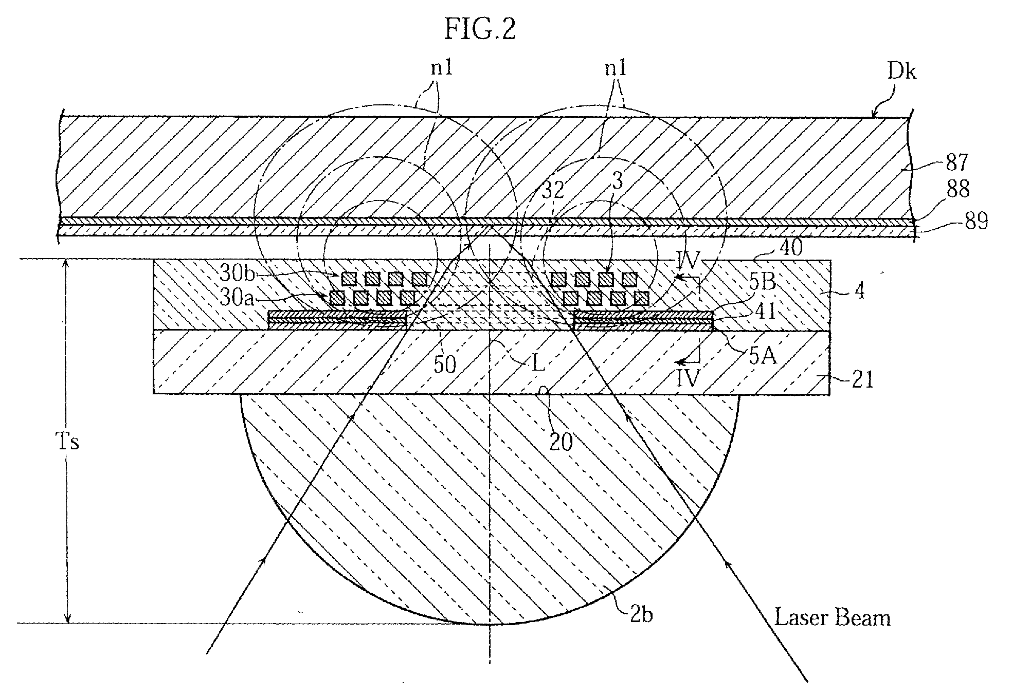
- the head Hd includes a lens holder 1, two objective lenses 2a ⁇ 2b held by the holder 1, a coil 3 for magnetic field generation, a dielectric 4 enclosing the coil 3, and two magnetic field regulators 5A ⁇ 5B.
- the lens holder 1 is supported by a carriage 60 movable in a tracking direction Tg (radially in respect of the disk Dk). To actuate the carriage 60 in the direction. Tg, use may be made of a voice coil motor (not shown). Appropriate movement of the carriage 60 in this direction (“seek operation") brings the lens holder 1 close to the desired track of the disk Dk. To enable tracking control, the lens holder 1 is mounted on the carriage 60 via a fine actuator (not shown). On being energized, the fine actuator minutely shifts the lens holder 1 in the tracking direction Tg. Further, the lens holder 1 can be moved in a focus direction Fs by an electromagnetic actuator 19.
- the disk Dk is rotated at high speed about the axis C1 (Fig. 1) by a spindle motor Ms.
- the disk Dk is made up of a transparent substrate 87, a recording layer 88 formed on one side of the substrate 87, and a transparent insulating layer 89 to protect the recording layer 88.
- the head Hd is held directly facing the recording layer 88 without intervention of the substrate 87 ("front illumination type").
- the recording apparatus Ra includes a stationary optical unit 7 made up of a laser diode 70, a collimating lens 71, a beam splitter 72, an optical detecting device 73, etc.
- the optical unit 7 emits a laser beam toward the carriage 60 in which a mirror 61 is provided.
- the emitted laser beam is reflected upward by the mirror 61, to pass through the objective lenses 2a, 2b.
- the laser beam is caused to converge by these lenses, thereby making a beam spot on the recording layer 88.
- the laser beam traces back the previous path. Then, the laser beam is received by the optical detecting device 73 in the optical unit 7.
- the objective lens 2b has a flat, upper lens surface 20 attached to a substrate 21.
- the lens 2b and the substrate 21 are both made of a transparent glass material and their refractive indexes are the same or substantially the same.
- a first magnetic field regulator 5A, a second magnetic field regulator 5B, a coil 3 and a dielectric 4 are provided on the substrate 21.
- the dielectric 4 which may be made of a transparent material such as alumina or silicon dioxide, has the same or substantially same refractive index as the substrate 21 (and hence the lens 2b). With the equality of refractive indexes, the combination of the lens 2b, the substrate 21 and the dielectric 4 serves as a single lens.
- This compound lens has a predetermined thickness Ts, as shown in Fig. 2.
- the coil 3 may be made by patterning a copper layer. Specifically, the "wafer process" known in the field of semiconductor device fabrication can be utilized in forming a prearranged copper layer into the required spiral.
- the coil 3 has a two-layer structure consisting of a first conductive spiral 30a and a second conductive spiral 30b.
- the central axis L of the coil 3 coincides with the axes of the objective lenses 2a, 2b.
- the coil 3 is connected to an external power source via conductive leads laid in the dielectric 4 or on the surface of the substrate 21.
- the two-layer structure of the coil 3 is not essential for an embodiment of the present invention, so that the coil 3 may consist of only one spiral or more than two spirals.
- the dielectric 4, enclosing the coil 3 and the magnetic field regulators 5A ⁇ 5B, has a flat surface held facing the disk Dk.
- the dielectric 4 fills the center of the coil 3, to provide a light-permeable portion 32 through which the laser beam passes.
- the inner diameter of the coil 3 is made as small as possible, while allowing enough room for the laser beam to pass.
- the magnetic field regulators 5A, 5B may have a thickness of 5 ⁇ m.
- the material that forms the field regulators 5A, 5B has a higher thermal conductivity than the material that forms the dielectric 4.
- the field regulators 5A, 5B can serve as a heat sink for dissipation of the heat generated at the coil 3.
- the field regulators 5A, 5B may be made of permalloy (nickel-iron alloy).
- the two field regulators 5A, 5B sandwich an intermediate layer 41 made of a dielectric material.
- the field regulators 5A, 5B are disposed between the coil 3 and the substrate 21. In other words, the field regulators 5A, 5B are opposite to the disk Dk, and the coil 3.
- the center of the respective field regulators 5A, 5B coincides with the center L of the coil 3.
- the assembly of the magnetic field regulators 5A, 5B is provided with a central hole 50 for passing the laser beam from the lens 2b.
- the magnetic field regulators 5A and 5B are divided by radially extending slits 51 into identical sectors 52a and 52b, respectively.
- the slits 51 are filled with dielectric material to enable electrical insulation of the sectors 52a (and the sectors 52b as well) .
- the dielectric material may be transparent or nontransparent.
- Fig. 4 shows a sectional view of the structure of the magnetic field regulators 5A, 5B taken along a line extending circumferentially of the regulator assembly shown in Fig. 3.
- the magnetic field regulator 5A and the magnetic field regulator 5B are the same in structure.
- the magnetic field regulator 5A is composed of a plurality of identical sectors 52a. As shown in Fig. 4, these sectors can be divided into two groups. A first group of sectors (designated as 52a') are disposed lower than a second group of sectors (designated as 52a"). The lower sectors 52a' alternate with the higher sectors 52a" in the circumferential direction of the regulator assembly. The first-group sectors 52a' are arranged on the substrate 21, while the second-group sectors 52a" are offset upward from the substrate 21.
- the sectors 52a' are electrically insulated from the sectors 52a" by a dielectric layer 42 that covers the upper surface and side surfaces of each sector 52a'.
- the dielectric layer 42 defines upwardly open recesses 42a in which the sectors 52a" are accommodated.
- the above-mentioned slits 51 correspond to the gaps between the sectors 52a' and the sectors 52a.
- the magnetic field regulator 5A (and the field regulator 5B as well) may be fabricated in the following manner.
- a titanium or chromium layer 59 as an undercoat is formed on a substrate 21 by vapor deposition or sputtering for example.
- the layer 59 may have a submicron thickness.
- a resist mask 58 is formed on the titanium layer 59.
- the uncovered portions of the layer 59 correspond in position to the sectors 52a' shown in Fig. 4.
- the gaps of the resist mask 58 are filled with a magnetic material (permalloy) 5A' by plating.
- the mask 58 is removed by e.g. washing, as shown in Fig. 5D.
- the exposed portions of the titanium layer 59 are removed by e.g. ion milling, as shown in Fig. 5E.
- the sectors 52a' are obtained.
- a dielectric layer 42 (made of alumina for example) is formed on the substrate 21 and on the sectors 52a' by e.g. sputtering.
- a titanium or chromium undercoat (like the one shown in Fig. 5A) is formed on the dielectric layer 42 by plating.
- a permalloy layer 5A" is formed by plating so that the recesses 42a are filled up.
- the surface of the permalloy layer 5A" is leveled by e.g. chemical mechanical polishing. The remaining portions of the layer 5A" serve as the sectors 52a" shown in Fig. 4.
- the plating for forming the sections 52a (52a' and 52a") of the field regulator 5A can be performed more readily and at lower cost than vapor deposition or sputtering. Further, in the above process, it is possible to form the first-group sections 52a' at a large pitch before forming the second-group sections 52a". Thus, the patterning for the sections 52a' can be performed readily. The latter formed second-group sections 52a" are reliably insulated from the first-group sections 52a' by the intermediate dielectric layer 42.
- the field regulator 5A After the field regulator 5A is made, an intermediate layer 41 is formed on the field regulator 5A. Then the field regulator 5B is fabricated in the same manner as the field regulator 5A.
- a high-frequency driving current (no less than 20 MHz for example) is supplied to the coil 3.
- the coil 3 Upon application of the current, the coil 3 generates a magnetic field (the sign n1 in Fig. 2 refers to lines of magnetic force).
- the direction of the lines of magnetic force is generally perpendicular to the recording layer 88.
- Some of the magnetic force lines enter the field regulators 5A, 5B.
- the magnetic flux density of the lines piercing the sectors 52a or 52b varies in the radial direction of the sectors.
- Fig. 6A illustrating a fan-shaped element 90 made of magnetic material.
- a clockwise electric current i is induced in the inner end of the element 90, thereby producing a magnetic field to act against the change in the density B .
- E the strength of the magnetic field induced within the element 90
- j the current density resulting from the magnetic field induction by j
- W the power consumption by W
- the power consumption W can be reduced by making smaller the strength E .
- the strength E and the magnetic flux density B satisfy the following equation (one of the four Maxwell equations).
- the area S may be reduced or the length l may be increased.
- a smaller fan-shaped magnetic element 90A is shown.
- the element 90A is an exact half of the element 90 described above.
- the area S' of the inner end is 1/2 of the area S of the element 90.
- the total circumferential length of the area S' is not reduced to half the circumferential length of the area S .
- the magnetic field for the smaller element 90A is weaker than that for the larger element 90 since the coefficient S / l of the equation (5) is smaller for the case of the element 90A than for the case of the element 90.
- the power consumption W can be made smaller.
- the power consumption in a fan-shaped magnetic element can be reduced by decreasing the width of the element (the size in a direction perpendicular to the magnetic flux).
- the magnetic flux adjustors 5A, 5B are divided into smaller sections 52a or 52b.
- the power consumption in the field regulators 5A, 5B is reduced, whereby the heat generation in them is reduced.
- an unacceptable temperature rise in the coil 3 is prevented.
- the width of the inner end (i.e., the minimum width) of the sectors 52a, 52b may be 5 ⁇ 10 ⁇ m when the thickness of the sectors is 5 ⁇ m.
- the ratio of the thickness to the minimum width is 1 to 1.
- the width of the inner end of each sector is also 5 ⁇ m. Supposing that the circumferential length of the hole 50 in the field regulators 5A ⁇ 5B is 500 ⁇ m and that the width of each slit 51 (see Fig. 3) is 2 ⁇ m, each of the magnetic field regulators 5A, 5B may be divided into 71 sectors to make the width of the inner end of each sector about 5 ⁇ m (500 ⁇ 71-2 ⁇ 5.0).
- the field regulators 5A, 5B have a higher thermal conductivity than the dielectric 4. Thus, they serve as an excellent heat sink for dissipation of the heat generated by the coil 3. As a result, it is possible to reliably control the temperature rise in the coil 3.
- the control of the temperature rise in the coil 3 contributes to prevention of the electromigration in the coil 3 and prevention of the increase in electric resistance of the coil 3. Accordingly, the power consumption in the magnetic head Hd is advantageously reduced. Further, since the temperature rise in the magnetic field regulators 5A, 5B is controlled, a higher-frequency driving current can be applied to the coil 3, whereby a high data transfer rate can be achieved.
- the magnetic field generating coil may be formed directly on the objective lens.
- the magnetic head in an embodiment of the present invention may be provided with a slider that floats slightly over the data storage disk in rotation. Further, the magnetic head in an embodiment of the present invention may not incorporate an objective lens.
Landscapes
- Engineering & Computer Science (AREA)
- Manufacturing & Machinery (AREA)
- Recording Or Reproducing By Magnetic Means (AREA)
- Magnetic Heads (AREA)
Abstract
Description


Claims (14)
- A magnetic head comprising:a coil (3) that generates a magnetic field and has an axis (L); anda magnetic member (5A, 5B) spaced from the coil (3) along said axis (L) and formed with a center hole (50); characterized in that the magnetic member (5A, 5B) includes a plurality of sections (52a, 52b) that are electrically insulated from each other and arranged around said axis (L).
- The magnetic head according to claim 1, wherein the sections (52a, 52b) are separated from each other by gaps (51) extending radially from said axis (L).
- The magnetic head according to claim 2, wherein each of the gaps (51) is filled with dielectric material (42).
- The magnetic head according to any one of claims 1∼3, wherein the magnetic member (5A, 5B) is positioned farther away from a data storage medium (Dk) than the coil (3) is.
- The magnetic head according to any one of claims 1∼4, further comprising a dielectric layer (4) that encloses the coil (3) and the magnetic member (5A, 5B).
- The magnetic head according to any one of claims 1∼5, wherein the sections (52a, 52b) have a minimum width that is no smaller than a thickness of the sections (52a, 52b) and no greater than twice the thickness of the sections (52a, 52b).
- The magnetic head according to any one of claims 1∼6, wherein the magnetic member (5A, 5B) comprises a first magnetic layer (5A) and a second magnetic layer (5B) that is stacked on the first magnetic layer (5A) via a dielectric layer (41).
- The magnetic head according to any one of claims 1∼7, further comprising an objective lens (2b) for forming a beam spot on a data storage medium (Dk).
- The magnetic head according to claim 8, wherein a light beam, after passing through the objective lens (2b) and before reaching the storage medium (Dk), passes through the center hole (50) of the magnetic member (5A, 5B) and a center of the coil (3).
- The magnetic head according to any one of claims 1∼9, wherein the sections (52a, 52b) are divided into a first group and a second group, the first group sections (52a') being arranged to alternate with the second group sections (52a") in a circumferential direction of the magnetic member (5A, 5B).
- The magnetic head according to claim 10, further comprising a dielectric film (42) covering the first group sections (52a'), wherein the dielectric film (42) provides a plurality of recesses (42a) between the first group sections (52a'), the recesses (42a) accommodating the second group sections (52a").
- A method of forming a magnetic member (5A, 5B) on a substrate (21), the magnetic member (5A, 5B) including a plurality of sections (52a, 52b) separated from each other, the method comprising the steps of:forming a plurality of first magnetic sections (52a') separated from each other on the substrate (21);forming a dielectric layer (42) on the substrate (21) to cover the first magnetic sections (52a') in a manner such that the dielectric layer (42) defines a plurality of recesses (42a) between the first magnetic sections (52a'); andforming a second magnetic section (52a") in each of the recesses 42a.
- The method according to claim 12, wherein the first and the second magnetic sections (52a', 52a") are formed by plating.
- A magneto-optical data recording apparatus comprising:characterized in that the magnetic member (5A, 5B) includes a plurality of sections (52a, 52b) that are electrically insulated from each other and arranged around said axis (L).a spindle motor (Ms) for rotating a magneto-optical data storage medium (Dk);a light source (7) for irradiating the storage medium (Dk) with a light beam;a magnetic head (Hd) that includes a magnetic field generating coil (3) and a magnetic member (5A, 5B), the coil (3) having an axis (L), the magnetic member (5A, 5B) being spaced from the coil (3) along said axis (L) and formed with a center hole (50); andan optical detector (73) that detects reflection light from the storage medium (Dk) and outputs a detection signal;
Applications Claiming Priority (2)
| Application Number | Priority Date | Filing Date | Title |
|---|---|---|---|
| JP2001360907A JP2003162850A (en) | 2001-11-27 | 2001-11-27 | Magnetic head, magneto-optical storage device, and method of forming magnetic layer |
| JP2001360907 | 2001-11-27 |
Publications (2)
| Publication Number | Publication Date |
|---|---|
| EP1315158A2 true EP1315158A2 (en) | 2003-05-28 |
| EP1315158A3 EP1315158A3 (en) | 2005-11-30 |
Family
ID=19171651
Family Applications (1)
| Application Number | Title | Priority Date | Filing Date |
|---|---|---|---|
| EP02251560A Withdrawn EP1315158A3 (en) | 2001-11-27 | 2002-03-06 | Magnetic head, data recording apparatus incorporating such a head and magnetic head fabrication method |
Country Status (3)
| Country | Link |
|---|---|
| US (1) | US6697305B2 (en) |
| EP (1) | EP1315158A3 (en) |
| JP (1) | JP2003162850A (en) |
Cited By (1)
| Publication number | Priority date | Publication date | Assignee | Title |
|---|---|---|---|---|
| WO2005015556A1 (en) * | 2003-08-08 | 2005-02-17 | Koninklijke Philips Electronics N.V. | Magnetic head for a magneto-optical device and magneto-optical device |
Families Citing this family (5)
| Publication number | Priority date | Publication date | Assignee | Title |
|---|---|---|---|---|
| IL157012A (en) * | 2003-07-17 | 2008-08-07 | Rafael Advanced Defense Sys | Temperature compensation device for optical instruments |
| JP2005141810A (en) * | 2003-11-05 | 2005-06-02 | Fujitsu Ltd | Magneto-optical head and magneto-optical disk apparatus |
| JP4185099B2 (en) * | 2003-11-06 | 2008-11-19 | 富士通株式会社 | Magneto-optical head |
| JP2005149665A (en) * | 2003-11-19 | 2005-06-09 | Fujitsu Ltd | Magneto-optical head and magneto-optical disk apparatus |
| KR100761205B1 (en) * | 2006-05-04 | 2007-09-21 | 후지쯔 가부시끼가이샤 | Magneto-optical head |
Family Cites Families (8)
| Publication number | Priority date | Publication date | Assignee | Title |
|---|---|---|---|---|
| FR2705488B1 (en) * | 1993-05-14 | 1995-06-23 | Commissariat Energie Atomique | Magnetic writing head for magneto-optical recording. |
| US5872693A (en) * | 1993-08-10 | 1999-02-16 | Kabushiki Kaisha Toshiba | Thin-film magnetic head having a portion of the upper magnetic core coplanar with a portion of the lower magnetic core |
| JPH0935937A (en) | 1995-05-17 | 1997-02-07 | Alps Electric Co Ltd | Inductive element |
| US5978320A (en) | 1997-05-16 | 1999-11-02 | Sony Corporation | Recording/reproducing apparatus for use with a photomagnetic recording medium |
| JPH10320863A (en) | 1997-05-19 | 1998-12-04 | Sony Corp | Recording and playback device |
| US6351436B1 (en) * | 1998-05-11 | 2002-02-26 | Maxtor Corporation | Field enhancing magnetic pole for magneto-optical recording and reproducing device |
| JP2001023260A (en) * | 1999-07-08 | 2001-01-26 | Sony Corp | Magnetic head for magnetic field modulation, magneto-optical element, optical pickup device, and optical disk device |
| US6781926B2 (en) * | 2000-10-10 | 2004-08-24 | Hitachi Maxell, Limited | Magneto-optical head having heat sink layer |
-
2001
- 2001-11-27 JP JP2001360907A patent/JP2003162850A/en active Pending
-
2002
- 2002-02-28 US US10/085,391 patent/US6697305B2/en not_active Expired - Fee Related
- 2002-03-06 EP EP02251560A patent/EP1315158A3/en not_active Withdrawn
Cited By (1)
| Publication number | Priority date | Publication date | Assignee | Title |
|---|---|---|---|---|
| WO2005015556A1 (en) * | 2003-08-08 | 2005-02-17 | Koninklijke Philips Electronics N.V. | Magnetic head for a magneto-optical device and magneto-optical device |
Also Published As
| Publication number | Publication date |
|---|---|
| EP1315158A3 (en) | 2005-11-30 |
| JP2003162850A (en) | 2003-06-06 |
| US6697305B2 (en) | 2004-02-24 |
| US20030099053A1 (en) | 2003-05-29 |
Similar Documents
| Publication | Publication Date | Title |
|---|---|---|
| TW577055B (en) | Magnetic head with improved heat dissipation properties | |
| KR100784396B1 (en) | Manufacturing method of magnetic head having flat coil | |
| JP2000036141A (en) | Flying optical head assembly and optical disk drive data storage system | |
| EP1039458A2 (en) | Optical head and coil assembly used for the same | |
| EP1315158A2 (en) | Magnetic head, data recording apparatus incorporating such a head and magnetic head fabrication method | |
| JPH05128618A (en) | Magnetooptic head and manufacture thereof | |
| JP3668189B2 (en) | Optical head and optical information processing apparatus | |
| US6529449B1 (en) | Magneto-optical head involving solid immersion lens with two-layer heat-dispersive coil | |
| US6760278B2 (en) | Magnetic head and data recording and reproduction device | |
| JP4185099B2 (en) | Magneto-optical head | |
| JP2002230860A (en) | Magneto-optical head and magneto-optical recording apparatus using the same | |
| KR100761205B1 (en) | Magneto-optical head | |
| US20050105402A1 (en) | Magneto-optical head and magneto-optical disk drive | |
| US6870806B2 (en) | Magnetic head provided with moment-reducing contact for data storage medium | |
| JP2005141810A (en) | Magneto-optical head and magneto-optical disk apparatus | |
| JP2004087068A (en) | Compound optical head and optical disk device using the same | |
| EP1528550B1 (en) | Magnetic field generator and magneto-optical information storage device | |
| JP3783367B2 (en) | Optical element for magneto-optical recording and recording / reproducing apparatus | |
| EP1570472A1 (en) | Magneto-optical device | |
| JP2006059487A (en) | Magneto-optical head and magneto-optical disk apparatus | |
| JP2005011400A (en) | Magnetic field generator and magneto-optical storage device | |
| WO2005057570A1 (en) | Magnetooptic head | |
| KR20050089745A (en) | Magnetic field generator and magneto-optical information storage device | |
| JP2003257099A (en) | Magnetic head, data recording / reproducing device, and magnetic film forming method for magnetic head |
Legal Events
| Date | Code | Title | Description |
|---|---|---|---|
| PUAI | Public reference made under article 153(3) epc to a published international application that has entered the european phase |
Free format text: ORIGINAL CODE: 0009012 |
|
| AK | Designated contracting states |
Designated state(s): AT BE CH CY DE DK ES FI FR GB GR IE IT LI LU MC NL PT SE TR |
|
| AX | Request for extension of the european patent |
Extension state: AL LT LV MK RO SI |
|
| PUAL | Search report despatched |
Free format text: ORIGINAL CODE: 0009013 |
|
| AK | Designated contracting states |
Kind code of ref document: A3 Designated state(s): AT BE CH CY DE DK ES FI FR GB GR IE IT LI LU MC NL PT SE TR |
|
| AX | Request for extension of the european patent |
Extension state: AL LT LV MK RO SI |
|
| AKX | Designation fees paid | ||
| REG | Reference to a national code |
Ref country code: DE Ref legal event code: 8566 |
|
| STAA | Information on the status of an ep patent application or granted ep patent |
Free format text: STATUS: THE APPLICATION IS DEEMED TO BE WITHDRAWN |
|
| 18D | Application deemed to be withdrawn |
Effective date: 20060531 |