EP1313213A2 - Wide common mode differential input amplifier and method - Google Patents
Wide common mode differential input amplifier and method Download PDFInfo
- Publication number
- EP1313213A2 EP1313213A2 EP02022427A EP02022427A EP1313213A2 EP 1313213 A2 EP1313213 A2 EP 1313213A2 EP 02022427 A EP02022427 A EP 02022427A EP 02022427 A EP02022427 A EP 02022427A EP 1313213 A2 EP1313213 A2 EP 1313213A2
- Authority
- EP
- European Patent Office
- Prior art keywords
- input
- pair
- amplifier
- transistor
- recited
- Prior art date
- Legal status (The legal status is an assumption and is not a legal conclusion. Google has not performed a legal analysis and makes no representation as to the accuracy of the status listed.)
- Granted
Links
- 238000000034 method Methods 0.000 title claims description 39
- 230000000295 complement effect Effects 0.000 claims description 21
- 239000004065 semiconductor Substances 0.000 claims description 13
- 230000003139 buffering effect Effects 0.000 claims description 4
- 239000000872 buffer Substances 0.000 description 14
- 102100036285 25-hydroxyvitamin D-1 alpha hydroxylase, mitochondrial Human genes 0.000 description 8
- 101000875403 Homo sapiens 25-hydroxyvitamin D-1 alpha hydroxylase, mitochondrial Proteins 0.000 description 8
- 238000013461 design Methods 0.000 description 7
- 238000004891 communication Methods 0.000 description 4
- 230000007812 deficiency Effects 0.000 description 2
- 230000011664 signaling Effects 0.000 description 2
- XUIMIQQOPSSXEZ-UHFFFAOYSA-N Silicon Chemical compound [Si] XUIMIQQOPSSXEZ-UHFFFAOYSA-N 0.000 description 1
- 230000005540 biological transmission Effects 0.000 description 1
- 238000010276 construction Methods 0.000 description 1
- 238000010586 diagram Methods 0.000 description 1
- 238000005516 engineering process Methods 0.000 description 1
- 238000007689 inspection Methods 0.000 description 1
- 238000012986 modification Methods 0.000 description 1
- 230000004048 modification Effects 0.000 description 1
- 238000012545 processing Methods 0.000 description 1
- 230000000630 rising effect Effects 0.000 description 1
- 229910052710 silicon Inorganic materials 0.000 description 1
- 239000010703 silicon Substances 0.000 description 1
- 238000012546 transfer Methods 0.000 description 1
Images



Classifications
-
- H—ELECTRICITY
- H03—ELECTRONIC CIRCUITRY
- H03F—AMPLIFIERS
- H03F3/00—Amplifiers with only discharge tubes or only semiconductor devices as amplifying elements
- H03F3/45—Differential amplifiers
- H03F3/45071—Differential amplifiers with semiconductor devices only
- H03F3/45479—Differential amplifiers with semiconductor devices only characterised by the way of common mode signal rejection
- H03F3/45632—Differential amplifiers with semiconductor devices only characterised by the way of common mode signal rejection in differential amplifiers with FET transistors as the active amplifying circuit
-
- H—ELECTRICITY
- H03—ELECTRONIC CIRCUITRY
- H03F—AMPLIFIERS
- H03F3/00—Amplifiers with only discharge tubes or only semiconductor devices as amplifying elements
- H03F3/45—Differential amplifiers
- H03F3/45071—Differential amplifiers with semiconductor devices only
- H03F3/45076—Differential amplifiers with semiconductor devices only characterised by the way of implementation of the active amplifying circuit in the differential amplifier
- H03F3/45179—Differential amplifiers with semiconductor devices only characterised by the way of implementation of the active amplifying circuit in the differential amplifier using MOSFET transistors as the active amplifying circuit
- H03F3/4521—Complementary long tailed pairs having parallel inputs and being supplied in parallel
- H03F3/45219—Folded cascode stages
-
- H—ELECTRICITY
- H03—ELECTRONIC CIRCUITRY
- H03F—AMPLIFIERS
- H03F3/00—Amplifiers with only discharge tubes or only semiconductor devices as amplifying elements
- H03F3/45—Differential amplifiers
- H03F3/45071—Differential amplifiers with semiconductor devices only
- H03F3/45076—Differential amplifiers with semiconductor devices only characterised by the way of implementation of the active amplifying circuit in the differential amplifier
- H03F3/45179—Differential amplifiers with semiconductor devices only characterised by the way of implementation of the active amplifying circuit in the differential amplifier using MOSFET transistors as the active amplifying circuit
- H03F3/45237—Complementary long tailed pairs having parallel inputs and being supplied in series
Definitions
- This invention relates to an input/output (I/O) interface circuitry for high speed integrated circuit (IC) applications. More specifically, it relates to the low voltage differential signaling input buffers that have a wide common mode input range and low power consumption.
- Differential drivers and receivers are well known. Differential drivers and receivers are used in many input/output (I/O) applications such as in communications, video and integrated circuits that may demand high data transfer rate. Differential drivers and receivers are used in integrated circuits (IC) for on-chip communications between circuits, chip-to-board, off-chip communications, etc.
- I/O input/output
- IC integrated circuits
- LVDS Low-voltage differential signaling
- LVDS interfaces have reduced voltage swing and can operate at very high speed with less power consumption. With differential outputs, a LVDS receiver can reject ambient common mode noise and less parallelism is needed due to the increased data rate of LVDS I/O drivers. Thus, the use of LVDS can reduce the overall cost and size of high speed ICs.
- LVDS requires a common mode input voltage that is substantially bounded by the supply voltages. This is often referred to as a rail-to-rail input voltage.
- CMOS Complementary Metal-Oxide-Semiconductor
- NMOS N-type Metal-Oxide-Semiconductor
- PMOS P-type Metal-Oxide-Semiconductor
- An NMOS transistor is turned ON when the gate voltage (Vg) is above the source voltage (Vs) by the threshold voltage (Vtn), or when Vg-Vs>Vtn. Since Vs is typically set to ground, to turn an NMOS transistor ON, it is required to have Vg>Vtn. If Vtn is in a range of 0.4V, the transistor will be OFF if the input Vg is near ground.
- a PMOS transistor is turned ON when the gate voltage is below the source voltage (Vs) by threshold voltage (Vtp), or when Vs-Vg>Vtp.
- Vs is typically the power supply voltage, VDD.
- Vtp threshold voltage
- Vg is typically the power supply voltage
- a prior art wide input range amplifier is shown in Fig. 5.
- the amplifier includes two input buffers B1 and B2, which may be implemented by a PMOS stage and an NMOS stage.
- the outputs of buffers B1 and B2 are combined in a MUX M1, which receives an input control signal from a Schmidtt trigger ANDed with the common mode voltage Vcm, via a third buffer B3.
- the control signal Z selects which output range to use, XP or XN. This is then input into the digital logic of the circuit.
- a wide input range amplifier including a first and second stage.
- the first stage has first and second inputs, first and second outputs, and first, second and third voltage sources.
- the first stage accepts input signals having a first common mode voltage range and outputs a first output signal having a second common mode voltage range and being amplified a first amount.
- the second stage has first and second inputs connected to the first and second outputs of the first stage, respectively.
- the second stage accepts input signals having a common mode voltage in the second range and outputs a second output signal having a third common mode voltage range and being amplified a second amount.
- a method of buffering an input signal including steps of providing a first amplifier stage for receiving an input signal having a first voltage range, amplifying the input signal a first amount, and outputting an output signal having a second voltage range being amplified said first amount.
- the method further includes steps of providing a second amplifier stage for receiving the output signal from said first amplifier stage, amplifying the output signal a second amount, and outputting a differential output signal having a third voltage range being amplified said second amount.
- a method for receiving a signal which includes the steps of receiving a thick device signal having a first common mode range; amplifying the thick device signal a first amount and stepping the thick device signal down to a first thin device signal having a second common mode range; and amplifying the thin device signal a second amount and outputting a second thin device signal having a third common mode voltage range.
- a wide input range amplifier which includes a first and second amplifying means.
- the first amplifying means for accepting input signals having a first common mode voltage range and outputting a first output signal having a second common mode voltage range and being amplified a first amount.
- the second amplifying means for accepting input signals having a common mode voltage in the second range and outputting a second output signal having a third common mode voltage range and being amplified a second amount.
- a thick device In a digital CMOS process, there are two types of devices in terms of gate oxide thickness. One is called a thick device and has a high threshold voltage, and another is called a thin device and has a low threshold voltage. For an example, in the 0.13 ⁇ digital process there are 2.5V and 1.2V devices. Thick devices are ideal for sustaining high voltage in the interface circuitry, and thin devices with low threshold devices are preferred for their high speed and lower power consumption, for digital core circuitry.
- an LVDS input buffer (receiver) is to accept a voltage signal from outside the chip or IC, and convert the signal to 1.2V logic for core processing.
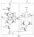
- Fig. 1 shows a two-stage wide common mode input buffer schematic.
- the buffer includes a pre-amplifier 10 stage and a Current Mode Logic (CML) stage 20.
- a first source voltage VDD1 is a 2.5V I/O voltage (thick device), and a second source voltage VDD2 is 1.2V core voltage (thin device) used for the digital core.
- a common mode voltage source Vcm is ideally set to (VDD1)/2, but in this case it can be 1.2V for practical reasons.
- the pre-amp stage 10 includes complementary input stages.
- a first PMOS stage (106 and 108) and a second NMOS stage (110 and 112) are used.
- the input buffer can accept wide input common voltages.
- NMOS transistor 104 provides bias current to NMOS transistors 110 and 112.
- NMOS transistor 104 has its gate tied to a bias control voltage 116.
- the gain that is generated by NMOS transistor 110 may be given by the formula: Gm(110) *R(118), where Gm(110) is the transconductance of NMOS transistor 110, and R(118) is the resistance of load resistor 118.
- NMOS transistors 110 and 112 may have the same size and characteristics.
- PMOS transistors 106 and 108 also have the same size and characteristics.
- Load resistors 118 and 120 act as load resistors and preferably have the same resistance.
- the current source is provided by PMOS 102, which has its gate tied to a bias control voltage 114.
- CML stage 20 may be a differential amplifier and include a PMOS output stage.
- Incoming data is supplied to input nodes Vinp and Vinn.
- Common mode voltage Vcm is typically set to a voltage near the middle of voltage source VDD1.
- the input range is limited by the common mode voltage Vcm.
- Vinp and Vinn are quite high (e.g., 1.8V-2.4V)
- both PMOS transistors 106 and 108 tend to be OFF.
- the NMOS stage, NMOS transistors 110 and 112 will be ON.
- both NMOS transistors 110 and 112 are OFF, and PMOS transistors 106 and 108 will remain ON
- complementary input stages achieve a wide common mode input voltage range.
- the common-mode input range is not rail-to-rail, this embodiment of the present invention provides a simple and low cost (i.e., smaller in size and takes up less silicon area) wide input range solution.
- NMOS transistor 204 In the second stage of the input buffer, Current Mode Logic 20, a current sink (source) is provided by an NMOS transistor 204, which is biased by a bias voltage 117.
- NMOS transistors 210 and 212 provide a differential gain which can be calculated by: Gm(210) * R(220) to the output nodes Vout1 and Vout2; where Gm(210) is the transconductance of transistor 210, and R(220) is the resistance of resistor 220.
- the second stage, CML stage 20 completes the voltage level shift from VDD1 to VDD2, at which the digital core operates.
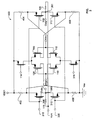
- Fig. 2 shows the schematic of a differential receiver pre-amp with rail-to-rail common mode input range according to another embodiment of the present invention.
- Pre-amp 300 uses cascoded structures to fold the gain to differential resistors.
- the second stage can be a CML stage or differential amplifier, such as CML 20, shown and described with reference to Fig 1.
- pre-amp 300 includes a complementary input pair, NMOS input stage (110 and 112) and PMOS input stage (106 and 108).
- Pre-amp 300 includes a current source, NMOS transistor 104 which provides bias current to the input NMOS transistor pair 110 and 112. The gate of the transistor 104 is controlled by bias control voltage 316.
- the inputs to the pre-amplifier 300 are Vinp and Vinn, and are connected to the gates of the input NMOS transistor pair 110 and 112 and to the gates of PMOS transistor pair 106 and 108.
- PMOS transistors 302 and 304 are current sources which provide proper bias current to PMOS transistors 306 and 308. The gates of transistor 306 and 308 are controlled by another bias voltage 318.
- the input NMOS pair 110 and 112 drive the differential resistors 118 and 120 through the cascoded transistors 306 and 308, which are cascoded with NMOS transistors 110 and 112, respectively.
- the load resistors 118 and 120 are also loaded to a common mode voltage Vcm.
- the common mode voltage may be set to near the middle of the supply voltage VDD1 or VDD1/2. For practical reasons, Vcm may be set to VDD2.
- the differential gain of this NMOS stage provides voltage gain of Gm(110)*R(120), at output nodes Outp and Outn.
- preamplifier 300 includes NMOS transistors 110 and 112 which can have the same size and characteristics, as do PMOS transistors 306 and 308, PMOS transistors 302 and 304, and differential resistors 118 and 120.
- the input PMOS pair 106 and 108 drive the differential resistors 118 and 120 through the cascaded NMOS transistors 310 and 312, where transistor 310 and 312 are biased from voltage 320.
- the bias current for the tail current 104 (current sink) is controlled by a bias voltage 316.
- Transistors 310 and 312 receive bias current from NMOS transistors 314 and 315, respectively.
- the differential gain of this stage is given by Gm(106)*R(118) at nodes Outn and Outp.
- transistors 106 and 108 have the same size and characteristics, as do transistors 310 and 312, and transistors 314 and 315.
- the common mode input voltage range can be designed in the following manner. When the inputs Vinp and Vinn are very high, only NMOS transistor pair 110 and 112 will be ON. To have NMOS transistors 110 and 112 in the saturation region, it is required to maintain: Vd(110) - Vs(110) > Vg(110) - Vs(110) - Vtn, where Vd(110) is the drain voltage (all referenced to ground (VSS)) for NMOS 110, Vs(110) is the source voltage, Vg(110) is the gate voltage, and Vtn is the threshold voltage of the NMOS transistor.
- transistors 306 and 308 should be biased through the bias voltage 318, so that Vd of transistors 110 and 112 are greater than (VDD1-Vtn).
- Vs(106) - Vd(106) > Vs(106) - Vg(106) - Vtp where Vs(106) is the source voltage referenced to ground VSS, Vd(106) is the drain voltage, Vg is the gate voltage, and Vtp is the threshold voltage for PMOS transistor 106.
- Vg(106) 0
- Vd(106) must be less than Vtp. This can be met by bias transistor 310 and 312 through the bias voltage 320.
- Fig. 3 shows another embodiment of a pre-amplifier with rail-to-rail common mode input voltage range according to the present invention.
- the second stage of the amplifier can be a current mode logic CML stage or differential amplifier as shown and described with reference to Fig. 1.
- the embodiment is very similar to the embodiment of Fig. 2.
- the main difference from the schematic of Fig. 2 is that the current source transistors 302,304, 314, and 315 are replaced with resistors 402, 404, 406, and 408.
- the operation of the circuit is very similar to that in Fig. 2, but the overall gain is reduced since the resistors 402-408 introduce load on the input pairs. In a typical implementation, the resistance of resistors 402-408 may be equal.
- a wide input stage buffers which perform level shifting from a high (I/O voltage) voltage to low voltage (digital core voltage).
- the buffer of the present invention includes a pre-amp stage and a differential amplifier stage.
- the differential output reduces duty cycle distortion.
- the wide input range pre-amp stages use complementary input pairs to accept wide input ranges. Cascoded stages may be used to improve input range.
- Fig. 4 is a flowchart of a method for receiving a wide input range input signal and stepping it to core voltage according to an embodiment of the present invention.
- the process begins at step S5-1.
- a pre-amplifier (first stage) including complementary input stages is provided.
- the complementary input stages may be configured such as described above with references to Figs. 1-3.
- the input stages may include a PMOS pair and an NMOS pair, only one of which will be on for a given voltage range.
- Each transistor of the input pairs may be cascoded in order to fold the gain to load resisters, as described with reference to Figs. 2-3.
- the pre-amplifier stage may configured to provide a gain to an input signal and also to reduce the common mode voltage range, so that an amplified output signal may be output at step S4-5 having an improved voltage range.
- the input signal may be within the LVDS standard range.
- a second stage amplifier may be provided to receive the output signal from the first stage amplifier, and may be configured as described in Fig. 1.
- the second stage amplifier may be designed to step the signal down for use in the digital core, and reduce the common mode voltage range to a negligible range for output at step S4-7. As already described above, this can be accomplished with a CML differential amplifier.
Landscapes
- Engineering & Computer Science (AREA)
- Power Engineering (AREA)
- Amplifiers (AREA)
Abstract
Description
Claims (45)
- A wide input range amplifier comprising:a first stage having first and second inputs, first and second outputs, and first, second and third voltage sources, said first stage accepting input signals having a first common mode voltage range and outputting a first output signal having a second common mode voltage range and being amplified a first amount;a second stage having first and second inputs connected to said first and second outputs of said first stage, respectively, said second stage accepting input signals having a common mode voltage in said second range and outputting a second output signal having a third common mode voltage range and being amplified a second amount.
- A wide input range amplifier as recited in claim 1, wherein:said first stage includes differential resistors loaded across said first and second outputs of said first stage, as a load of said first stage.
- A wide input range amplifier as recited in claim 2, wherein said first stage includes two input stages, said two input stages including a first inputs stage of a first conductive type and a second input stage of a second conductive type.
- A wide input range amplifier as recited in any preceding claim, wherein said second stage comprises a differential amplifier.
- A wide input range amplifier as recited in any preceding claim, wherein said second stage comprises a current mode logic differential amplifier.
- A wide input range amplifier as recited in any one of claims 1-4, wherein said second stage includes a common source differential amplifier.
- A wide input range amplifier as recited in claim 3, wherein said first input stage comprises complementary input stages.
- A wide input range amplifier as recited in claim 7, wherein said complementary input stages comprise a first input stage of a first semi-conductor type, and a second input stage of a second semi-conductor type.
- A wide input range amplifier as recited in claim 8, wherein said first input stage comprises a P-type coupled pair biased with a first current source, and said second input stage comprises an N-type coupled pair biased with a second current source.
- A wide input range amplifier as recited in claim 1, wherein said first stage comprises a P-type common source pair connected to a first current source and an N-type common source pair connected to a second current source, and first and second differential resistors, and wherein said first current source is connected to said first voltage source, said second current source is connected to said second voltage source, a gate of a first transistor of said P-type common source pair being connected to said first input, a gate of a second transistor of said P-type common source pair being connected to said second input, a gate of a first transistor of said N-type common source pair being connected to said first input, a gate of a second transistor of said N-type common source pair being connected to said second input, a drain of said first transistor of said P-type common source pair being connected to said first output, a drain of said second transistor of said P-type common source pair being connected to said second output, a drain of said first transistor of said N-type common source pair being connected to said first output, a drain of said second transistor of said N-type common source pair being connected to said second input, and said pair of load resistors being connected two each other and two said first and second outputs, and said mid-point of said pair of load resistors being connected to said third voltage source.
- A wide input range amplifier as recited in claim 10, wherein said third voltage source supplies approximately half of a voltage of said first voltage source, and said second voltage source is ground.
- A wide input range amplifier as recited in claim 1, wherein said first stage further comprises complementary first and second input pairs, first and second differential resistors, and a first and second pair of cascoded transistors, and wherein
said first input pair is of a first semi-conductor type and said second input pair is of a second semi-conductor type, and said load resistors are loaded across said first and second outputs as load resistors. - A wide input range amplifier as recited in claim 12, wherein said first input pair is biased by a first current source, said second input pair is biased by a second current source, a first and second transistor of said first cascoded pair is biased by a third and fourth current source respectively, a first and second transistor of said second cascoded pair is biased by a fifth and sixth current source respectively, said first cascoded pair is cascoded to an output of said second input pair, and said second cascoded pair is cascoded to an output of said first input pair .
- A wide input range amplifier as recited in claim 13, wherein a drain of a first transistor of said first input pair is connected to a source of a first transistor of said second cascoded pair, a drain of a second transistor of said first input pair is connected to a source of a second transistor of said second cascoded pair, a drain of a first transistor of said second input pair is connected to a source of a second transistor of said first cascoded pair, and a drain of a second transistor of said second input pair is connected to a source of a second transistor of said first cascoded pair.
- A wide input range amplifier as recited in any one of claims 11-14, wherein said first voltage source has a voltage approximately twice that of said third voltage source, and said second voltage source is ground.
- A wide input range amplifier as recited in any one of claims 10-15, wherein said first and second differential resistors comprise active load transistors.
- A wide input range amplifier as recited in claim 13, wherein said third and fourth current sources each comprise a transistor of a first semi-conductor type connected to said first voltage source, and said third and fourth current sources each comprise a transistor of a second semi-conductor type connected to said second voltage source.
- A wide input range amplifier as recited in claim 13, further comprising a first, second, third and fourth bias voltage, said first bias voltage biasing said first, third and fourth current sources, said second bias voltage biasing said first cascoded pair, aid third bias voltage biasing said second cascoded pair, and said fourth bias voltage biasing said second, fifth and sixth current sources.
- A method of buffering an input signal, said method comprising:providing a first amplifier stage for receiving an input signal having a first voltage range, amplifying said input signal a first amount, and outputting an output signal having a second voltage range being amplified said first amount;providing a second amplifier stage for receiving said output signal from said first amplifier stage, amplifying said output signal a second amount, and outputting a differential output signal having a third voltage range being amplified said second amount.
- A method as recited in claim 19, wherein said providing a first amplifier stage step comprises:providing complementary input pairs for receiving said input signal,configuring a first input pair of said complementary input pairs to be OFF and a second input pair of said complementary input pairs to be ON, when said input signal is above a first input voltage, andconfiguring said first input pair of said complementary input pairs to be ON and said second input pair of said complementary input pairs to be OFF, when said input signal is below a first input voltage.
- A method as recited in claim 19, wherein said providing a first amplifier stage step comprises:providing first and second differential resistors as a load across the output of said first amplifier stage.
- A method as recited in claim 20, wherein said providing a first amplifier stage step further comprises:providing a first cascoded pair between the output of said first amplifier stage and cascoded with an output of said second input pair, andproviding a second cascoded pair between the output of said first amplifier stage and cascoded with an output of said first input pair.
- A method as recited in claim 20, wherein said providing complementary input pairs step comprises:providing said first input pair being a first semi-conductor type, andproviding said second input pair being a second semi-conductor type.
- A method as recited in any one of claims 19-23, wherein said providing a second amplifier stage step comprises providing a differential amplifier for receiving said output signal from said first amplifier stage.
- A method as recited in any one of claims 19-24, wherein said providing a second amplifier stage step comprises providing a current mode logic differential amplifier for receiving said output signal from said first amplifier stage.
- A method as recited in any one of claims 19-24, wherein said providing a second amplifier stage step comprises providing a common source differential amplifier for receiving said output signal from said first amplifier stage.
- A method as recited in claim 19, wherein said providing a first amplifier stage step further comprises:providing a P-type common source pair connected to a first current source and an N-type common source pair connected to a second current source, and first and second differential resistors,loading said first and second differential resistors across said output of said first stage amplifier,connecting said first current source to a first voltage source,connecting said second current source to a second voltage source,connecting a gate of a first transistor of said P-type common source pair to said first input,connecting a gate of a second transistor of said P-type common source pair to said second input,connecting a gate of a first transistor of said N-type common source pair to said first input,connecting a gate of a second transistor of said N-type common source pair to said second input,connecting a drain of said first transistor of said P-type common source pair to said first output,connecting a drain of said second transistor of said P-type common source pair to said second output,connecting a drain of said first transistor of said N-type common source pair to said first output,connecting a drain of said second transistor of said N-type common source pair to said second input,connecting said first and second differential resistors to each other and to said first and second outputs, andconnecting a mid-point of said first and second differential resistors to a third voltage source.
- A method as recited in claim 27, wherein said providing a first amplifier stage step further comprises setting said third voltage source to a voltage approximately half of that of said first voltage source, and
setting said second voltage source to ground. - A method as recited in claim 19, wherein said providing a first amplifier stage step further comprises:providing complementary first and second input pairs, said first input pair is of a first semi-conductor type and said second input pair is of a second semi-conductor type, providing first and second differential resistors connected across said output of said first amplifier stage as load resistors, andproviding a first and second pair of cascoded transistors, said first pair of cascoded transistors cascoded with said second input pair, and said second pair of cascoded transistor cascoded with said first input pair.
- A method as recited in claim 29, wherein said providing a first amplifier stage step further comprises:biasing said first input pair with a first current source, biasing said second input pair with a second current source,biasing a first and second transistor of said first cascoded pair with a third and fourth current source respectively, andbiasing a first and second transistor of said second cascoded pair with a fifth and sixth current source respectively.
- A method as recited in claim 30, wherein said providing a first amplifier stage step further comprises:connecting a drain of a first transistor of said first input pair to a source of a first transistor of said second cascoded pair,connecting a drain of a second transistor of said first input pair to a source of a second transistor of said second cascoded pair,connecting a drain of a first transistor of said second input pair to a source of a second transistor of said first cascoded pair, andconnecting a drain of a second transistor of said second input pair to a source of a second transistor of said first cascoded pair.
- A method as recited in claim 29, wherein said providing a first amplifier stage step further comprises:providing said first voltage source having a voltage approximately twice that of said third voltage source, and said second voltage source is ground.
- A method as recited in any one of claims 27 to 32, wherein said providing a first amplifier stage step further comprises:providing active load transistors as said first and second differential resistors.
- A method for receiving a signal, said method comprising the steps of:receiving a thick device signal having a first common mode range;amplifying said thick device signal a first amount and stepping said thick device signal down to a first thin device signal having a second common mode range; andamplifying said thin device signal a second amount and outputting a second thin device signal having a third common mode voltage range.
- A method as recited in claim 34, wherein said step of amplifying said thick device signal includes steps of:determining whether said first common mode range is above or below a threshold voltage, andamplifying said thick device signal a first amount and stepping said thick device signal down to said first thin device signal based on the determination.
- A method as recited in claim 34, wherein said step of amplifying said thin device signal includes a step of folding gain of said thin device signal to differential transistors to produce said second thin device signal as a differential output.
- A method as recited in claim 36, further comprising a step of outputting said differential output to a core digital system.
- A method as recited in claim 35, wherein said steps of determining whether said first common mode range is above or below a threshold voltage, and said step of amplifying said thick device signal include using complementary input pairs, a first pair of said complementary input pairs performing said step of amplifying said thick device signal when said first common mode range is above said threshold voltage, and a second pair of said complementary input pairs performing said step of amplifying said thick device signal when said first common mode range is below said threshold voltage.
- A method as recited in claim 36, wherein said step of folding gain of said thin device signal to differential transistors includes using at least one cascoded amplifier to perform said step of folding.
- A wide input range amplifier comprising:a first amplifying means for accepting input signals having a first common mode voltage range and outputting a first output signal having a second common mode voltage range and being amplified a first amount;a second amplifying means for accepting input signals having a common mode voltage in said second range and outputting a second output signal having a third common mode voltage range and being amplified a second amount.
- A wide input range amplifier as recited in claim 40, wherein:said first amplifying means includes a differential resistor means for providing a load of said first amplifying means.
- A wide input range amplifier as recited in claim 41, wherein said first amplifying means includes a first input stage of a first conductive type and a second input stage of a second conductive type.
- A wide input range amplifier as recited in claim 40, wherein said second amplifying means comprises a differential amplifying means for producing a differential signal.
- A wide input range amplifier as recited in claim 40, wherein said second amplifying means comprises a current mode logic differential amplifying means for producing a differential signal for digital core logic.
- A wide input range amplifier as recited in claim 40, wherein said second common mode voltage range approximate half said first common mode voltage range, and said third common mode voltage range is negligible.
Applications Claiming Priority (4)
| Application Number | Priority Date | Filing Date | Title |
|---|---|---|---|
| US33152201P | 2001-11-19 | 2001-11-19 | |
| US331522P | 2001-11-19 | ||
| US10/101,056 US6788142B2 (en) | 2001-11-19 | 2002-03-20 | Wide common mode differential input amplifier and method |
| US101056 | 2002-03-20 |
Publications (3)
| Publication Number | Publication Date |
|---|---|
| EP1313213A2 true EP1313213A2 (en) | 2003-05-21 |
| EP1313213A3 EP1313213A3 (en) | 2004-01-28 |
| EP1313213B1 EP1313213B1 (en) | 2010-03-24 |
Family
ID=26797853
Family Applications (1)
| Application Number | Title | Priority Date | Filing Date |
|---|---|---|---|
| EP02022427A Expired - Lifetime EP1313213B1 (en) | 2001-11-19 | 2002-10-04 | Wide common mode differential input amplifier and method |
Country Status (4)
| Country | Link |
|---|---|
| US (2) | US6788142B2 (en) |
| EP (1) | EP1313213B1 (en) |
| AT (1) | ATE462224T1 (en) |
| DE (1) | DE60235741D1 (en) |
Cited By (3)
| Publication number | Priority date | Publication date | Assignee | Title |
|---|---|---|---|---|
| CN101064503B (en) * | 2006-04-30 | 2010-05-12 | 中芯国际集成电路制造(上海)有限公司 | Wide Input Common Mode Voltage Comparator and Low Common Mode Voltage Comparator |
| CN102983822A (en) * | 2012-09-18 | 2013-03-20 | 上海集成电路研发中心有限公司 | Power amplifier |
| CN103873032A (en) * | 2014-03-17 | 2014-06-18 | 上海华虹宏力半导体制造有限公司 | Rail to rail input hysteresis comparator |
Families Citing this family (41)
| Publication number | Priority date | Publication date | Assignee | Title |
|---|---|---|---|---|
| US6803801B2 (en) * | 2002-11-07 | 2004-10-12 | Lsi Logic Corporation | CMOS level shifters using native devices |
| US7180333B2 (en) * | 2003-05-20 | 2007-02-20 | Avago Technologies General Ip (Singapore) Pte. Ltd. | Current mode logic driver that employs a level shifting mechanism |
| US7030695B2 (en) * | 2003-07-02 | 2006-04-18 | Sigmatel, Inc. | Low threshold voltage circuit employing a high threshold voltage output stage |
| KR101157224B1 (en) * | 2004-05-03 | 2012-06-15 | 엘지디스플레이 주식회사 | Liquid crystal display device |
| US7573331B2 (en) * | 2004-10-06 | 2009-08-11 | Agere Systems Inc. | Low power low noise amplifier for a magnetoresistive sensor |
| US7256651B1 (en) * | 2005-01-12 | 2007-08-14 | National Semiconductor Corporation | System and method for providing a constant swing high-gain complementary differential limiting amplifier |
| JP4291295B2 (en) * | 2005-04-08 | 2009-07-08 | エルピーダメモリ株式会社 | Logic circuit |
| KR100682056B1 (en) * | 2005-07-01 | 2007-02-15 | 삼성전자주식회사 | Buffer amplifier |
| US7352207B2 (en) * | 2005-09-30 | 2008-04-01 | Silicon Laboratories Inc. | Output driver with common mode feedback |
| US7348809B2 (en) * | 2006-03-23 | 2008-03-25 | Silicon Laboratories Inc. | Input buffer |
| US7508264B1 (en) * | 2006-04-14 | 2009-03-24 | Atheros Communications, Inc. | DC-couples RF multi-stage amplifier |
| US7508235B2 (en) * | 2006-06-07 | 2009-03-24 | Silicon Laboratories Inc. | Differential line termination technique |
| US7474133B1 (en) | 2006-12-05 | 2009-01-06 | National Semiconductor Corporation | Apparatus and method for high-speed serial communications |
| US7477077B1 (en) | 2006-12-05 | 2009-01-13 | National Semiconductor Corporation | Apparatus and method for loss of signal detection in a receiver |
| US7639043B2 (en) * | 2007-10-05 | 2009-12-29 | Winbond Electronics Corp. | LVDS receiver circuit |
| US7619475B2 (en) * | 2008-03-04 | 2009-11-17 | Ralink Technology (Singapore) Corporation | Cancellation of common mode oscillation in RF circuits |
| US7999523B1 (en) | 2008-08-29 | 2011-08-16 | Silicon Laboratories Inc. | Driver with improved power supply rejection |
| US20100117703A1 (en) * | 2008-11-13 | 2010-05-13 | Zhipeng Zhu | Multi-mode single-ended cmos input buffer |
| US8461880B2 (en) * | 2009-04-02 | 2013-06-11 | Silicon Labs Spectra, Inc. | Buffer with an output swing created using an over-supply voltage |
| KR101153601B1 (en) * | 2009-11-23 | 2012-06-15 | 삼성전기주식회사 | Power amplifier |
| EP2498398B1 (en) | 2011-03-07 | 2019-10-30 | Nxp B.V. | Amplifier circuit and method |
| US9356570B2 (en) * | 2014-05-15 | 2016-05-31 | Texas Instruments Deutschland Gmbh | High speed, rail-to-rail CMOS differential input stage |
| US10044362B2 (en) * | 2014-06-19 | 2018-08-07 | Texas Instruments Incorporated | Complementary current reusing preamp for operational amplifier |
| KR101675573B1 (en) * | 2016-03-21 | 2016-11-11 | 주식회사 이노액시스 | Level Shifter, Digital Analog Converter, Buffer Amplifier and Source Driver and Electronic Device Including the Same |
| US10461742B2 (en) * | 2016-09-01 | 2019-10-29 | Novatek Microelectronics Corp. | Chip, selectable mode buffer circuit and mode selecting method thereof |
| TWI634340B (en) * | 2016-12-30 | 2018-09-01 | 友達光電股份有限公司 | Integrated circuit structure, display device module and detection method thereof |
| US10224886B2 (en) | 2017-05-19 | 2019-03-05 | Novatek Microelectronics Corp. | Operational amplifier circuit using variable bias control |
| US10326411B2 (en) * | 2017-05-19 | 2019-06-18 | Novatek Microelectronics Corp. | Operational amplifier circuit capable of improving linearity relation between loading current and input voltage difference |
| KR102438388B1 (en) * | 2017-08-24 | 2022-08-31 | 삼성전자주식회사 | Signal amplifier, and signal receiving circuit and device comprising the same |
| CN111628732B (en) * | 2019-02-28 | 2023-10-10 | 晶豪科技股份有限公司 | Class D power amplifier circuit |
| US11223354B2 (en) | 2019-08-28 | 2022-01-11 | Stmicroelectronics International N.V. | Low current, wide range input common mode LVDS receiver devices and methods |
| EP3843098B1 (en) * | 2019-12-23 | 2025-03-05 | IMEC vzw | Sign switching circuitry |
| US11424716B2 (en) | 2020-12-21 | 2022-08-23 | Western Digital Technologies, Inc. | Dual voltage high speed receiver with toggle mode |
| US12160204B2 (en) | 2021-02-02 | 2024-12-03 | Macronix International Co., Ltd. | High-speed, low distortion receiver circuit |
| CN115549646B (en) * | 2021-06-30 | 2026-02-17 | 深圳市中兴微电子技术有限公司 | Clock receiving circuit and electronic device |
| CN115567045A (en) * | 2021-07-01 | 2023-01-03 | 上海禾赛科技有限公司 | Continuous Time Comparator and LiDAR System |
| CN114389553B (en) * | 2021-08-16 | 2023-01-24 | 美垦半导体技术有限公司 | Amplifier circuit, chip and household appliance |
| CN114221641B (en) * | 2022-02-21 | 2022-05-20 | 成都芯翼科技有限公司 | Rapid comparator circuit for wide common-mode input voltage |
| CN116488596B (en) * | 2023-01-19 | 2025-07-04 | 眸芯科技(上海)有限公司 | LVDS receiving circuit and chip with wide input common mode range |
| CN118694321A (en) * | 2023-03-24 | 2024-09-24 | 华为技术有限公司 | Operational amplifiers, chips, electronic devices |
| US12470438B2 (en) | 2023-07-03 | 2025-11-11 | Novatek Microelectronics Corp. | Low voltage differential signaling receiver |
Family Cites Families (11)
| Publication number | Priority date | Publication date | Assignee | Title |
|---|---|---|---|---|
| US5323120A (en) * | 1993-01-05 | 1994-06-21 | Sgs-Thomson Microelectronics, Inc. | High swing operational transconductance amplifier |
| US5381112A (en) * | 1993-09-22 | 1995-01-10 | Motorola, Inc. | Fully differential line driver circuit having common-mode feedback |
| US5734297A (en) * | 1996-03-29 | 1998-03-31 | Philips Electronics North America Corporation | Rail-to-rail input stages with constant gm and constant common-mode output currents |
| US5767698A (en) | 1996-06-06 | 1998-06-16 | International Business Machines Corporation | High speed differential output driver with common reference |
| US6118438A (en) | 1997-03-18 | 2000-09-12 | Ati Technologies, Inc. | Low comment mode impedence differential driver and applications thereof |
| US6107882A (en) * | 1997-12-11 | 2000-08-22 | Lucent Technologies Inc. | Amplifier having improved common mode voltage range |
| US6275107B1 (en) | 1998-10-29 | 2001-08-14 | Fujitisu Limited | Differential amplifier circuit and pull up-type differential driver |
| US6194962B1 (en) * | 1999-04-13 | 2001-02-27 | Analog Devices, Inc. | Adaptive operational amplifier offset voltage trimming system |
| KR100322539B1 (en) * | 1999-07-10 | 2002-03-18 | 윤종용 | Sense amplifying apparatus of semiconductor integrated circuit |
| US6525607B1 (en) * | 2000-09-27 | 2003-02-25 | Intel Corporation | High-voltage differential input receiver |
| US6252435B1 (en) | 2000-10-05 | 2001-06-26 | Pericom Semiconductor Corp. | Complementary differential amplifier with resistive loads for wide common-mode input range |
-
2002
- 2002-03-20 US US10/101,056 patent/US6788142B2/en not_active Expired - Lifetime
- 2002-10-04 AT AT02022427T patent/ATE462224T1/en not_active IP Right Cessation
- 2002-10-04 EP EP02022427A patent/EP1313213B1/en not_active Expired - Lifetime
- 2002-10-04 DE DE60235741T patent/DE60235741D1/en not_active Expired - Lifetime
-
2004
- 2004-03-19 US US10/804,169 patent/US6956436B2/en not_active Expired - Lifetime
Cited By (4)
| Publication number | Priority date | Publication date | Assignee | Title |
|---|---|---|---|---|
| CN101064503B (en) * | 2006-04-30 | 2010-05-12 | 中芯国际集成电路制造(上海)有限公司 | Wide Input Common Mode Voltage Comparator and Low Common Mode Voltage Comparator |
| CN102983822A (en) * | 2012-09-18 | 2013-03-20 | 上海集成电路研发中心有限公司 | Power amplifier |
| CN103873032A (en) * | 2014-03-17 | 2014-06-18 | 上海华虹宏力半导体制造有限公司 | Rail to rail input hysteresis comparator |
| CN103873032B (en) * | 2014-03-17 | 2016-11-16 | 上海华虹宏力半导体制造有限公司 | Track to track input hysteresis comparator |
Also Published As
| Publication number | Publication date |
|---|---|
| EP1313213A3 (en) | 2004-01-28 |
| US6956436B2 (en) | 2005-10-18 |
| DE60235741D1 (en) | 2010-05-06 |
| US20040174215A1 (en) | 2004-09-09 |
| US6788142B2 (en) | 2004-09-07 |
| US20030095003A1 (en) | 2003-05-22 |
| EP1313213B1 (en) | 2010-03-24 |
| ATE462224T1 (en) | 2010-04-15 |
Similar Documents
| Publication | Publication Date | Title |
|---|---|---|
| EP1313213B1 (en) | Wide common mode differential input amplifier and method | |
| EP0908005B1 (en) | Differential amplifier | |
| EP2498398B1 (en) | Amplifier circuit and method | |
| US7560957B2 (en) | High-speed CML circuit design | |
| US5754078A (en) | Operational amplifier for class B amplification | |
| US7453299B1 (en) | Programmable amplifiers with positive and negative hysteresis | |
| US7639043B2 (en) | LVDS receiver circuit | |
| US7339421B2 (en) | Differential circuit and receiver with same | |
| US7119600B2 (en) | Wide common mode high-speed differential receiver using thin and thick gate oxide MOSFETS in deep-submicron technology | |
| EP1251640A2 (en) | A low voltage differential to single-ended converter | |
| US6320422B1 (en) | Complementary source coupled logic | |
| US7843236B2 (en) | Low voltage differential signal receiver | |
| CN100530966C (en) | Low Voltage Differential Signaling (LVDS) receiver | |
| US7388406B2 (en) | CML circuit devices having improved headroom | |
| US20060012429A1 (en) | Self biased differential amplifier | |
| JP3888955B2 (en) | Receiver circuit | |
| US7342418B2 (en) | Low voltage differential signal receiver | |
| JP2002344260A (en) | Input rail-to-rail differential amplifier circuit | |
| US8456196B2 (en) | High-speed comparator | |
| EP0746929A1 (en) | High speed differential receiver for data communications | |
| JP2002314399A (en) | Semiconductor integrated circuit | |
| US6556074B2 (en) | Differential amplifying circuit and multi-stage differential amplifying circuit using the same | |
| TWI917060B (en) | Source follower circuit and flipped source follower circuit | |
| JP2003224460A (en) | Receiver circuit | |
| US6680626B2 (en) | High speed differential receiver |
Legal Events
| Date | Code | Title | Description |
|---|---|---|---|
| PUAI | Public reference made under article 153(3) epc to a published international application that has entered the european phase |
Free format text: ORIGINAL CODE: 0009012 |
|
| AK | Designated contracting states |
Designated state(s): AT BE BG CH CY CZ DE DK EE ES FI FR GB GR IE IT LI LU MC NL PT SE SK TR |
|
| AX | Request for extension of the european patent |
Extension state: AL LT LV MK RO SI |
|
| PUAL | Search report despatched |
Free format text: ORIGINAL CODE: 0009013 |
|
| AK | Designated contracting states |
Kind code of ref document: A3 Designated state(s): AT BE BG CH CY CZ DE DK EE ES FI FR GB GR IE IT LI LU MC NL PT SE SK TR |
|
| AX | Request for extension of the european patent |
Extension state: AL LT LV MK RO SI |
|
| 17P | Request for examination filed |
Effective date: 20040728 |
|
| AKX | Designation fees paid |
Designated state(s): AT BE BG CH CY CZ DE DK EE ES FI FR GB GR IE IT LI LU MC NL PT SE SK TR |
|
| RAP1 | Party data changed (applicant data changed or rights of an application transferred) |
Owner name: BROADCOM CORPORATION |
|
| 17Q | First examination report despatched |
Effective date: 20070515 |
|
| GRAP | Despatch of communication of intention to grant a patent |
Free format text: ORIGINAL CODE: EPIDOSNIGR1 |
|
| GRAS | Grant fee paid |
Free format text: ORIGINAL CODE: EPIDOSNIGR3 |
|
| GRAA | (expected) grant |
Free format text: ORIGINAL CODE: 0009210 |
|
| AK | Designated contracting states |
Kind code of ref document: B1 Designated state(s): AT BE BG CH CY CZ DE DK EE ES FI FR GB GR IE IT LI LU MC NL PT SE SK TR |
|
| REG | Reference to a national code |
Ref country code: GB Ref legal event code: FG4D |
|
| REG | Reference to a national code |
Ref country code: CH Ref legal event code: EP |
|
| REG | Reference to a national code |
Ref country code: IE Ref legal event code: FG4D |
|
| REF | Corresponds to: |
Ref document number: 60235741 Country of ref document: DE Date of ref document: 20100506 Kind code of ref document: P |
|
| REG | Reference to a national code |
Ref country code: NL Ref legal event code: VDEP Effective date: 20100324 |
|
| PG25 | Lapsed in a contracting state [announced via postgrant information from national office to epo] |
Ref country code: AT Free format text: LAPSE BECAUSE OF FAILURE TO SUBMIT A TRANSLATION OF THE DESCRIPTION OR TO PAY THE FEE WITHIN THE PRESCRIBED TIME-LIMIT Effective date: 20100324 Ref country code: FI Free format text: LAPSE BECAUSE OF FAILURE TO SUBMIT A TRANSLATION OF THE DESCRIPTION OR TO PAY THE FEE WITHIN THE PRESCRIBED TIME-LIMIT Effective date: 20100324 |
|
| PG25 | Lapsed in a contracting state [announced via postgrant information from national office to epo] |
Ref country code: ES Free format text: LAPSE BECAUSE OF FAILURE TO SUBMIT A TRANSLATION OF THE DESCRIPTION OR TO PAY THE FEE WITHIN THE PRESCRIBED TIME-LIMIT Effective date: 20100705 Ref country code: EE Free format text: LAPSE BECAUSE OF FAILURE TO SUBMIT A TRANSLATION OF THE DESCRIPTION OR TO PAY THE FEE WITHIN THE PRESCRIBED TIME-LIMIT Effective date: 20100324 Ref country code: GR Free format text: LAPSE BECAUSE OF FAILURE TO SUBMIT A TRANSLATION OF THE DESCRIPTION OR TO PAY THE FEE WITHIN THE PRESCRIBED TIME-LIMIT Effective date: 20100625 Ref country code: SE Free format text: LAPSE BECAUSE OF FAILURE TO SUBMIT A TRANSLATION OF THE DESCRIPTION OR TO PAY THE FEE WITHIN THE PRESCRIBED TIME-LIMIT Effective date: 20100324 Ref country code: BE Free format text: LAPSE BECAUSE OF FAILURE TO SUBMIT A TRANSLATION OF THE DESCRIPTION OR TO PAY THE FEE WITHIN THE PRESCRIBED TIME-LIMIT Effective date: 20100324 Ref country code: NL Free format text: LAPSE BECAUSE OF FAILURE TO SUBMIT A TRANSLATION OF THE DESCRIPTION OR TO PAY THE FEE WITHIN THE PRESCRIBED TIME-LIMIT Effective date: 20100324 |
|
| PG25 | Lapsed in a contracting state [announced via postgrant information from national office to epo] |
Ref country code: SK Free format text: LAPSE BECAUSE OF FAILURE TO SUBMIT A TRANSLATION OF THE DESCRIPTION OR TO PAY THE FEE WITHIN THE PRESCRIBED TIME-LIMIT Effective date: 20100324 Ref country code: CZ Free format text: LAPSE BECAUSE OF FAILURE TO SUBMIT A TRANSLATION OF THE DESCRIPTION OR TO PAY THE FEE WITHIN THE PRESCRIBED TIME-LIMIT Effective date: 20100324 Ref country code: BG Free format text: LAPSE BECAUSE OF FAILURE TO SUBMIT A TRANSLATION OF THE DESCRIPTION OR TO PAY THE FEE WITHIN THE PRESCRIBED TIME-LIMIT Effective date: 20100624 |
|
| PLBE | No opposition filed within time limit |
Free format text: ORIGINAL CODE: 0009261 |
|
| STAA | Information on the status of an ep patent application or granted ep patent |
Free format text: STATUS: NO OPPOSITION FILED WITHIN TIME LIMIT |
|
| PG25 | Lapsed in a contracting state [announced via postgrant information from national office to epo] |
Ref country code: PT Free format text: LAPSE BECAUSE OF FAILURE TO SUBMIT A TRANSLATION OF THE DESCRIPTION OR TO PAY THE FEE WITHIN THE PRESCRIBED TIME-LIMIT Effective date: 20100726 Ref country code: DK Free format text: LAPSE BECAUSE OF FAILURE TO SUBMIT A TRANSLATION OF THE DESCRIPTION OR TO PAY THE FEE WITHIN THE PRESCRIBED TIME-LIMIT Effective date: 20100324 |
|
| 26N | No opposition filed |
Effective date: 20101228 |
|
| PG25 | Lapsed in a contracting state [announced via postgrant information from national office to epo] |
Ref country code: IT Free format text: LAPSE BECAUSE OF FAILURE TO SUBMIT A TRANSLATION OF THE DESCRIPTION OR TO PAY THE FEE WITHIN THE PRESCRIBED TIME-LIMIT Effective date: 20100324 |
|
| PG25 | Lapsed in a contracting state [announced via postgrant information from national office to epo] |
Ref country code: MC Free format text: LAPSE BECAUSE OF NON-PAYMENT OF DUE FEES Effective date: 20101031 |
|
| REG | Reference to a national code |
Ref country code: CH Ref legal event code: PL |
|
| PG25 | Lapsed in a contracting state [announced via postgrant information from national office to epo] |
Ref country code: CH Free format text: LAPSE BECAUSE OF NON-PAYMENT OF DUE FEES Effective date: 20101031 Ref country code: LI Free format text: LAPSE BECAUSE OF NON-PAYMENT OF DUE FEES Effective date: 20101031 Ref country code: FR Free format text: LAPSE BECAUSE OF NON-PAYMENT OF DUE FEES Effective date: 20101102 |
|
| REG | Reference to a national code |
Ref country code: FR Ref legal event code: ST Effective date: 20110630 |
|
| PG25 | Lapsed in a contracting state [announced via postgrant information from national office to epo] |
Ref country code: IE Free format text: LAPSE BECAUSE OF NON-PAYMENT OF DUE FEES Effective date: 20101004 |
|
| PG25 | Lapsed in a contracting state [announced via postgrant information from national office to epo] |
Ref country code: CY Free format text: LAPSE BECAUSE OF FAILURE TO SUBMIT A TRANSLATION OF THE DESCRIPTION OR TO PAY THE FEE WITHIN THE PRESCRIBED TIME-LIMIT Effective date: 20100324 |
|
| PG25 | Lapsed in a contracting state [announced via postgrant information from national office to epo] |
Ref country code: LU Free format text: LAPSE BECAUSE OF NON-PAYMENT OF DUE FEES Effective date: 20101004 |
|
| PG25 | Lapsed in a contracting state [announced via postgrant information from national office to epo] |
Ref country code: TR Free format text: LAPSE BECAUSE OF FAILURE TO SUBMIT A TRANSLATION OF THE DESCRIPTION OR TO PAY THE FEE WITHIN THE PRESCRIBED TIME-LIMIT Effective date: 20100324 |
|
| REG | Reference to a national code |
Ref country code: DE Ref legal event code: R082 Ref document number: 60235741 Country of ref document: DE Representative=s name: BOSCH JEHLE PATENTANWALTSGESELLSCHAFT MBH, DE Ref country code: DE Ref legal event code: R081 Ref document number: 60235741 Country of ref document: DE Owner name: AVAGO TECHNOLOGIES INTERNATIONAL SALES PTE. LT, SG Free format text: FORMER OWNER: BROADCOM CORP., IRVINE, CALIF., US Ref country code: DE Ref legal event code: R081 Ref document number: 60235741 Country of ref document: DE Owner name: AVAGO TECHNOLOGIES GENERAL IP (SINGAPORE) PTE., SG Free format text: FORMER OWNER: BROADCOM CORP., IRVINE, CALIF., US |
|
| REG | Reference to a national code |
Ref country code: GB Ref legal event code: 732E Free format text: REGISTERED BETWEEN 20171005 AND 20171011 |
|
| REG | Reference to a national code |
Ref country code: DE Ref legal event code: R081 Ref document number: 60235741 Country of ref document: DE Owner name: AVAGO TECHNOLOGIES INTERNATIONAL SALES PTE. LT, SG Free format text: FORMER OWNER: AVAGO TECHNOLOGIES GENERAL IP (SINGAPORE) PTE. LTD., SINGAPORE, SG Ref country code: DE Ref legal event code: R082 Ref document number: 60235741 Country of ref document: DE Representative=s name: BOSCH JEHLE PATENTANWALTSGESELLSCHAFT MBH, DE |
|
| REG | Reference to a national code |
Ref country code: GB Ref legal event code: 732E Free format text: REGISTERED BETWEEN 20190222 AND 20190227 |
|
| PGFP | Annual fee paid to national office [announced via postgrant information from national office to epo] |
Ref country code: GB Payment date: 20191028 Year of fee payment: 18 |
|
| PGFP | Annual fee paid to national office [announced via postgrant information from national office to epo] |
Ref country code: DE Payment date: 20201031 Year of fee payment: 19 |
|
| GBPC | Gb: european patent ceased through non-payment of renewal fee |
Effective date: 20201004 |
|
| PG25 | Lapsed in a contracting state [announced via postgrant information from national office to epo] |
Ref country code: GB Free format text: LAPSE BECAUSE OF NON-PAYMENT OF DUE FEES Effective date: 20201004 |
|
| REG | Reference to a national code |
Ref country code: DE Ref legal event code: R119 Ref document number: 60235741 Country of ref document: DE |
|
| PG25 | Lapsed in a contracting state [announced via postgrant information from national office to epo] |
Ref country code: DE Free format text: LAPSE BECAUSE OF NON-PAYMENT OF DUE FEES Effective date: 20220503 |