EP1313031A2 - Interpolator - Google Patents
Interpolator Download PDFInfo
- Publication number
- EP1313031A2 EP1313031A2 EP02256364A EP02256364A EP1313031A2 EP 1313031 A2 EP1313031 A2 EP 1313031A2 EP 02256364 A EP02256364 A EP 02256364A EP 02256364 A EP02256364 A EP 02256364A EP 1313031 A2 EP1313031 A2 EP 1313031A2
- Authority
- EP
- European Patent Office
- Prior art keywords
- digital image
- interpolation
- coefficient
- input digital
- equation
- Prior art date
- Legal status (The legal status is an assumption and is not a legal conclusion. Google has not performed a legal analysis and makes no representation as to the accuracy of the status listed.)
- Withdrawn
Links
Images



Classifications
-
- H—ELECTRICITY
- H04—ELECTRIC COMMUNICATION TECHNIQUE
- H04N—PICTORIAL COMMUNICATION, e.g. TELEVISION
- H04N7/00—Television systems
- H04N7/01—Conversion of standards, e.g. involving analogue television standards or digital television standards processed at pixel level
-
- G—PHYSICS
- G06—COMPUTING OR CALCULATING; COUNTING
- G06T—IMAGE DATA PROCESSING OR GENERATION, IN GENERAL
- G06T3/00—Geometric image transformations in the plane of the image
- G06T3/40—Scaling of whole images or parts thereof, e.g. expanding or contracting
- G06T3/4007—Scaling of whole images or parts thereof, e.g. expanding or contracting based on interpolation, e.g. bilinear interpolation
-
- H—ELECTRICITY
- H04—ELECTRIC COMMUNICATION TECHNIQUE
- H04N—PICTORIAL COMMUNICATION, e.g. TELEVISION
- H04N5/00—Details of television systems
- H04N5/14—Picture signal circuitry for video frequency region
-
- G—PHYSICS
- G06—COMPUTING OR CALCULATING; COUNTING
- G06T—IMAGE DATA PROCESSING OR GENERATION, IN GENERAL
- G06T2200/00—Indexing scheme for image data processing or generation, in general
- G06T2200/28—Indexing scheme for image data processing or generation, in general involving image processing hardware
Definitions
- the present invention relates to an interpolator for digital image processing comprising a processor for providing an interpolated pixel value from a plurality of input values according to a predetermined function and coefficient providing means for proving a coefficient value to the processor for use in the application of said function;.
- Figure 1 shows a conventional apparatus which processes digital images.
- digital image pixel data is input from a frame store memory (not shown) to the apparatus for digital image processing.
- the input digital image pixel data is interpolated by the apparatus, which processes the digital image, and output to a printer (not shown) or stored in another frame store memory (not shown) for later processing.
- the conventional image processing apparatus includes a controller 100, a vertical direction interpolation coefficient memory 101, a vertical direction interpolation input buffer 103, a vertical direction interpolation circuit 105, a vertical direction interpolation output buffer 107, a horizontal direction interpolation circuit 109, and a horizontal direction interpolation coefficient memory 111.
- the controller 100 controls the vertical direction interpolation coefficient memory 101, the vertical direction interpolation input buffer 103, the vertical direction interpolation circuit 105, the vertical direction interpolation output buffer 107, the horizontal direction interpolation circuit 109, and the horizontal direction interpolation coefficient memory 111, so as to interpolate pixel values of the input digital image.
- the vertical direction interpolation input buffer 103 temporarily stores the pixel values of the input digital image, and is embodied on a First-In First-Out (FIFO) basis.
- FIFO is a method of processing program operation requests which processes a first request first (i.e. a firstly-input pixel value of the digital image).
- At least one interpolation coefficient used by an equation that represents a position of an output pixel, i.e. an interpolation node, is stored in the vertical direction interpolation coefficient memory 101 and the horizontal direction interpolation coefficient memory 111.
- the interpolation coefficients of the respective output pixel positions are calculated according to a distance between the pixel values of the input digital image, an increment interval between the pixel positions of the output digital image, and an interpolation method in the respective output pixel positions.
- a series of the pixel values of the input digital image are multiplied by the corresponding interpolation coefficients, thereby interpolating the pixel values of the input digital image.
- the vertical direction interpolation circuit 105 When a vertical direction interpolation processing signal is received by the controller 100, the vertical direction interpolation circuit 105 obtains vertical direction interpolation coefficients corresponding to the pixel values of the input digital image from the vertical direction interpolation coefficient memory 101, respectively multiplies the pixel values of the digital image by the vertical direction interpolation coefficients corresponding to the pixel values, and calculates a sum of the resulting values to perform the vertical direction interpolation.
- the pixel values of the digital image interpolated in a vertical direction by the vertical direction interpolation circuit 105 are stored in the vertical direction interpolation output buffer 107.
- the horizontal direction interpolation circuit 109 receives the pixel values of the digital image interpolated in a vertical direction from the vertical direction interpolation output buffer 107. In addition, the horizontal direction interpolation circuit 109 obtains horizontal direction interpolation coefficients corresponding to the pixel values of the input digital image from the horizontal direction interpolation coefficient memory 111. Thereafter, the horizontal direction interpolation circuit 109 respectively multiplies the pixel values of the digital image interpolated in the vertical direction by the horizontal direction interpolation coefficients obtained from the horizontal direction interpolation coefficient memory 111, and calculates a sum of the resulting values to perform the horizontal direction interpolation. Accordingly, the horizontal and vertical direction interpolations of the pixel values of the input digital image are completed.
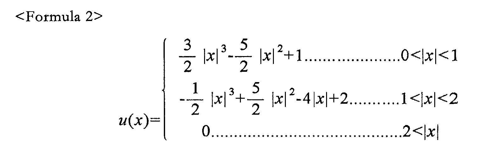
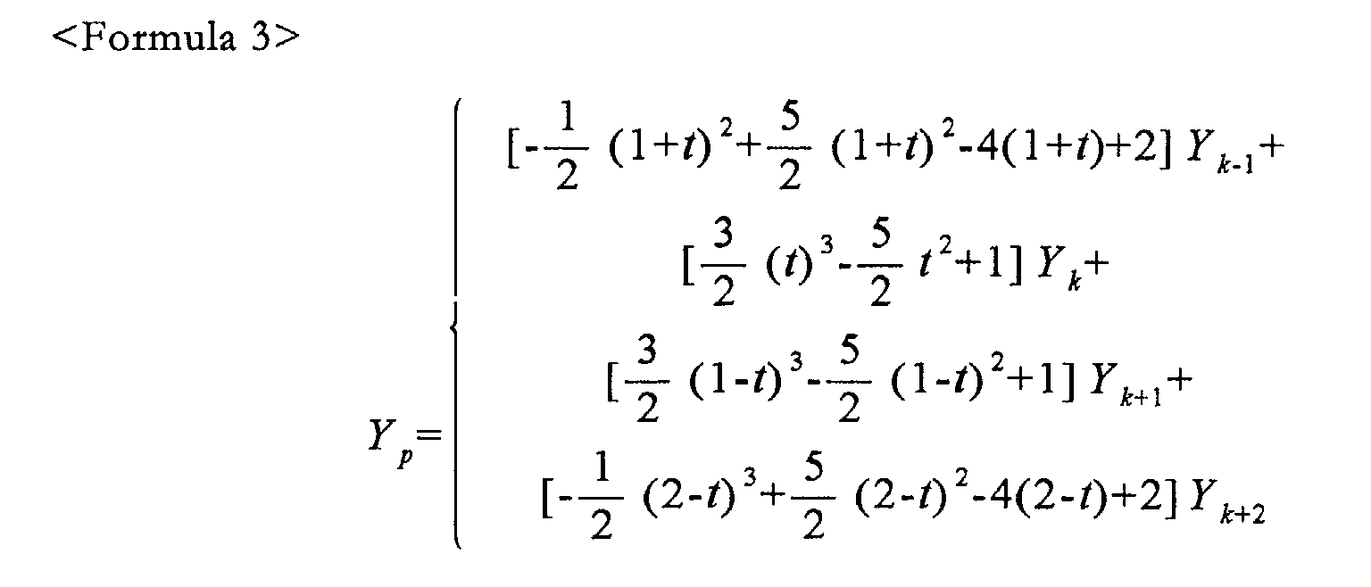
- Figure 3 illustrates an interpolation method by the cubic convolution of Figure 2. Assuming that an interval of the respective periods is '1', an interpolation node Y P is represented by Formula 3 according to a boundary condition:
- Formula 4 is obtained by processing Formula 3 as a function of 't'.
- Y k-1 , Y k , Y k+1 and Y k+2 indicate positions of k-1, k, k+1 and k+2-th sampled output pixels of the input digital image, respectively.
- Y p ⁇ (Y k+2 - 3Y k+1 + 3Y k - Y k-1 )/2 ⁇ t 3 + ⁇ (-Y k+2 + 4Y k+1 -5Y k +2Y k-1 )/2 ⁇ t 2 + ⁇ (Y k+2 -2Y k-1 )/2 ⁇ t + Y k
- the respective coefficients C 1 , C 2 , C 3 and C 4 can be obtained from a lookup table.
- a bank is generally used as shown in Figure 5.
- the bank is a logical unit which divides a main memory device for management. The bank is used to prepare for an increase of the main memory device or to utilize a limited memory device space by bank switching. The more banks are used, the higher the performance.
- the respective banks contain representative values, thus generating errors. For example, when values between 0 and 1 are divided between five banks, the values are divided at an interval of 0.2.
- a distance 't' between 0 and 1 in the cubic convolution filter is set up to be 0.1, to calculate the values C 1 , C 2 , C 3 and C 4 . Accordingly, values between 0 and 0.2 are approximated to 0.1, which may generate an error.
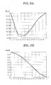
- Figures 6A, 6B, 6C and 6D illustrate an error distribution of the cubic convolution of Figure 3 and probable errors of the respective coefficients.
- the coefficients are divided by 1/N periods during N bank periods, and an error value of each period is reduced due to an increase of N.
- the interpolated pixel values have bigger errors. For example, assuming that 't' is 0.19 and the pixel value of the digital image represented by (255 255 1 1) belongs to a first bank, the representative value of 't' becomes 0.1, and thus the interpolated pixel value becomes 283. However, since 't' is 0.19, the interpolated pixel value calculated by using the actual 't' is 216. Accordingly, an error value of 67 is generated between the pixel value interpolated by the representative value of 't' of the bank and the pixel value interpolated by the actual 't'.
- Figure 7 shows a flowchart illustrating a conventional method of processing a digital image.
- the controller 100 calculates a size ratio of the pixel value of the input digital image to an aimed pixel value to be interpolated by the vertical direction interpolation circuit 105 and the horizontal direction interpolation circuit 109 in operation 1001. That is, when the horizontal direction is X and the vertical direction is Y, X scale is X size of the original digital image / X size of the aimed digital image, and Y scale is Y size of the original digital image / Y size of the aimed digital image.
- the controller 100 After calculating X and Y scales, the controller 100 measures Y k-1 , Y k , Y k+1 and Y k+2 in operation 1003.
- Y k-1 , Y k , Y k+1 and Y k+2 indicate positions of the k-1, k, k+1 and k+2-th sampled output pixels of the input digital image, respectively.
- the controller 100 After measuring Y k-1 , Y k , Y k+1 and Y k+2 , the controller 100 obtains 't' from the scale size in operation 1005.
- 't' represents an X axis interval between the pixel value of the input digital image and the interpolation node, namely an interpolation interval.
- the controller 100 After calculating 't', the controller 100 obtains coefficients from the corresponding memories, the vertical direction interpolation coefficient memory 101 and the horizontal direction interpolation coefficient memory 111 according to 't' in operation 1007. As described above, the vertical direction interpolation coefficient memory 101 and the horizontal direction interpolation coefficient memory 111 store the coefficients for variables which indicate the positions of the output pixels sampled in the interpolation node calculation equation.
- the controller 100 calculates the interpolation node Y P according to the obtained coefficient in operation 1009. In addition, the controller 100 interpolates the input digital image by using the calculated interpolation node in operation 1011. Accordingly, interpolation of the input digital image is completed.
- the conventional apparatus which processes the digital image and the method therefor require many adders and multipliers in a form of hardware, and also require many banks to obtain precise values. Moreover, when the number of banks is restricted, the respective banks store imprecise representative values for the interpolation intervals. As a result, errors are generated between the theoretical interpolated pixel values and those actually obtained and used.
- An interpolator is characterised in that the coefficient providing means is configured to calculate said coefficient as a coefficient calculation function of the interpolation interval, said coefficient calculation function itself being selected in dependence on the interpolation interval.
- said predetermined function is a cubic function.
- a digital image processing apparatus includes a controller 200, a horizontal direction interpolation input buffer 203, a horizontal direction interpolation circuit 205, a horizontal direction interpolation output buffer 207, and a vertical direction interpolation circuit 209.
- the controller 200 includes a register 200a.
- the controller 200 controls the horizontal direction interpolation input buffer 203, the horizontal direction interpolation circuit 205, the horizontal direction interpolation output buffer 207, and the vertical direction interpolation circuit 209, so as to interpolate between pixel values of the input digital image.
- the controller 200 measures an interpolation interval (t) for the pixel values of the input digital image, and performs operations for interpolating the digital image by using the measured interpolation interval.
- the horizontal direction interpolation input buffer 203 the horizontal direction interpolation circuit 205, the horizontal direction interpolation output buffer 207, and the vertical direction interpolation circuit 209 have similar functions as those shown in Figure 1, explanations thereof are omitted to avoid repetition. However, the respective elements 203, 205, 207 and 209 have different processing procedures.
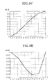
- the register 200a is installed in the controller 200, and stores a coefficient equation. As illustrated in Figures 9A, 9B, 9C and 9D, the coefficient equation uses a relationship that errors have linearity when coefficients of a cubic convolution are embodied as banks.
- Figures 9A through 9D are graphs showing C 1 , C 2 , C 3 and C 4 , respectively.
- the controller 200 calculates a size ratio of the pixel value of the input digital image to an aimed pixel value to be interpolated by the horizontal direction interpolation circuit 205 and the vertical direction interpolation circuit 209 in operation 2001. That is, when the horizontal direction is X and the vertical direction is Y, X scaling factor is X size of the original digital image / X size of the aimed digital image, and Y scaling factor is Y size of the original digital image / Y size of the aimed digital image.
- the controller 200 After calculating the X and Y scaling factors, the controller 200 measures Y k-1 , Y k , Y k+1 and Y k+2 in operation 2003.
- Y k-1 , Y k , Y k+1 and Y k+2 indicate positions of the k-1, k, k+1 and k+2th sampled pixels of the input digital image, respectively.
- the controller 200 After measuring Y k-1 , Y k , Y k+1 and Y k+2 , the controller 200 obtains 't' from the scale size in operation 2005.
- ' t ' represents an X axis interval between the pixel value of the input digital image and the interpolation node, namely an interpolation interval.
- the controller 200 After calculating ' t ', the controller 200 obtains a corresponding coefficient equation from the register 200a according to ' t ' in operation 2007. As described above, the register 200a stores the coefficient equations for each coefficient in the interpolation node calculation equation, and is provided in the controller 200. The amount of information stored in the register 200a corresponds to the predetermined coefficient equations, thereby reducing a processing time of the controller 200.
- the controller 200 calculates the coefficient from the coefficient equation in operation 2009, and obtains the interpolation node Yp by using the obtained coefficient in operation 2011. That is, the controller 200 transmits an interpolation node calculation signal to the horizontal direction interpolation circuit 205 and the vertical direction interpolation circuit 209, multiplies the coefficients from the register 200a by the pixel values of the input digital image, respectively, and calculates a sum of the resulting values, thereby performing the horizontal and vertical direction interpolations in operation 2013.
- Y p denotes the interpolation node of the input digital image
- Y n denotes a position of an n-th sampled output pixel of the input digital image
- C n is the coefficient of the position of the nth sampled pixel of the input digital image
- 'n 2,3,4, ..., n, ....'
- the controller 200 interpolates the input digital image by using the calculated interpolation node in operation 2130. Accordingly, interpolation of the pixel values of the input digital image is completed.
- the coefficient equation is represented by a linear equation according to the relationship that the range of the errors by N banks has linearity, thereby reducing the error of the interpolated value of the pixel value of the input digital image.
- a large number of adders and multipliers is not needed, further simplifying the structure of the digital image processing apparatus.
- the coefficient equation is stored in the register 200a of the controller 200 to reduce the processing time of the controller 200.
Landscapes
- Engineering & Computer Science (AREA)
- Multimedia (AREA)
- Signal Processing (AREA)
- Physics & Mathematics (AREA)
- General Physics & Mathematics (AREA)
- Theoretical Computer Science (AREA)
- Image Processing (AREA)
- Studio Circuits (AREA)
- Television Signal Processing For Recording (AREA)
- Complex Calculations (AREA)
- Editing Of Facsimile Originals (AREA)
Abstract
Description

Claims (24)
- An interpolator for digital image processing comprising:characterised in thata processor (205, 209) for providing an interpolated pixel value from a plurality of input values according to a predetermined function; andcoefficient providing means (200) for proving a coefficient value to the processor for use in the application of said function;
the coefficient providing means (200) is configured to calculate said coefficient as a coefficient calculation function of the interpolation interval, said coefficient calculation function itself being selected in dependence on the interpolation interval. - An interpolator according to claim 1, wherein said coefficient calculation function is of the form:
- An interpolator according to claim 1 or 2, wherein said predetermined function is a cubic function.
- An apparatus for processing a digital image, comprising:a register which stores a coefficient equation;an interpolation processing unit which interpolates the input digital image; anda controller which:measures an interpolation interval of pixel values of the digital image,calculates a coefficient by substituting the interpolation interval for the coefficient equation stored in the register,calculates an interpolation node for the digital image by substituting the coefficient, and an output pixel position value of the digital image for an interpolation node calculation equation, andcontrols the interpolation processing unit to interpolate the digital image to the interpolation node.
- The apparatus of claim 4, wherein the coefficient equation satisfies the following relationship:
- The apparatus of claim 5, wherein the interpolation node calculation equation satisfies the following relationship:
- A method of processing a digital image, the method comprising:measuring an interpolation interval of pixel values of the input digital image; calculating a coefficient by substituting the interpolation interval for a coefficient equation stored in a register;calculating an interpolation node for the digital image by substituting the coefficient and an output pixel position value of the digital image for an interpolation node calculation equation; andcontrolling an interpolation processing unit to interpolate the digital image to the interpolation node.
- The method of claim 7, wherein the coefficient equation satisfies the following relationship:
- The method of claim 8, wherein the interpolation node calculation equation satisfies the following relationship:
- The method of claim 9, wherein the coefficient equation is stored in the register and has linearity so as to reduce a processing time of the digital image and prevent errors in the interpolated digital image.
- The method of claim 7, wherein the measuring of the interpolation interval comprises:calculating a size ratio of the pixel values of the input digital image to aimed pixel values;measuring positions of sampled output pixels of the input digital image; and obtaining the interpolation interval according to the size ratio and the positions of the sampled output pixels.
- The method of claim 11, further comprising selecting the coefficient equation according to the interpolation interval among stored coefficient equations in the register for each coefficient in the interpolation node calculation equation.
- The method of claim 12, wherein the coefficient equation is stored in the register and has linearity so as to reduce a processing time of the digital image and prevent errors in the interpolated digital image.
- The apparatus of claim 1, further comprising:a horizontal direction interpolation input buffer which stores the pixel values of the input digital image;a horizontal direction interpolation circuit which performs a horizontal direction interpolation to the input digital image;a horizontal direction interpolation output buffer which stores the pixel values of the input digital image that are interpolated in the horizontal direction interpolation circuit; andvertical direction interpolation circuit which performs a vertical direction interpolation to the input digital image.
- The apparatus of claim 14, wherein the controller selects the coefficient equation according to the interpolation interval among stored coefficient equations in the register for each coefficient in the interpolation node calculation equation.
- The apparatus of claim 15, wherein the coefficient equation is stored in the register and has linearity so as to reduce a processing time of the digital image and prevent errors in the interpolated digital image.
- The apparatus of claim 4, wherein the coefficient equation and errors of the coefficient equation have linearity so as to reduce a number of adders and multipliers, where the coefficient equation is embodied in a form of hardware.
- The apparatus of claim 4, wherein the register is stored in the controller.
- The apparatus of claim 7, wherein the coefficient equation is stored in the register and has linearity so as to reduce a processing time of the digital image and prevent errors in the interpolated digital image.
- A computer readable medium encoded with operating instructions for implementing a method of processing a digital image by a computer, the method comprising:measuring an interpolation interval of pixel values of the input digital image; calculating a coefficient by substituting the interpolation interval for a coefficient equation stored in a register data set;calculating an interpolation node for the digital image by substituting the coefficient and an output pixel position value of the digital image for an interpolation node calculation equation; andcontrolling an interpolation processing unit to interpolate the digital image to the interpolation node.
- The computer readable medium of claim 20, wherein the measuring of the interpolation interval comprises:calculating a size ratio of the pixel values of the input digital image to aimed pixel values;measuring positions of sampled output pixels of the input digital image; and obtaining the interpolation interval according to the size ratio and the positions of the sampled output pixels.
- The computer readable medium of claim 20, further comprising selecting the coefficient equation according to the interpolation interval among stored coefficient equations in the register data set for each coefficient in the interpolation node calculation equation.
- The computer readable medium of claim 20, wherein the coefficient equation satisfies the following relationship:
- The computer readable medium of claim 23, wherein the interpolation node calculation equation satisfies the following relationship:
Applications Claiming Priority (2)
| Application Number | Priority Date | Filing Date | Title |
|---|---|---|---|
| KR10-2001-0056935A KR100423503B1 (en) | 2001-09-14 | 2001-09-14 | Apparatus for disposing digital image and a method using the same |
| KR2001056935 | 2001-09-14 |
Publications (2)
| Publication Number | Publication Date |
|---|---|
| EP1313031A2 true EP1313031A2 (en) | 2003-05-21 |
| EP1313031A3 EP1313031A3 (en) | 2005-02-23 |
Family
ID=19714304
Family Applications (1)
| Application Number | Title | Priority Date | Filing Date |
|---|---|---|---|
| EP02256364A Withdrawn EP1313031A3 (en) | 2001-09-14 | 2002-09-13 | Interpolator |
Country Status (5)
| Country | Link |
|---|---|
| US (1) | US7110620B2 (en) |
| EP (1) | EP1313031A3 (en) |
| JP (1) | JP3869779B2 (en) |
| KR (1) | KR100423503B1 (en) |
| TW (1) | TW581978B (en) |
Families Citing this family (11)
| Publication number | Priority date | Publication date | Assignee | Title |
|---|---|---|---|---|
| JP2005331603A (en) * | 2004-05-18 | 2005-12-02 | Sony Corp | Image processing apparatus and method |
| JP4774736B2 (en) * | 2004-12-27 | 2011-09-14 | カシオ計算機株式会社 | Image enlargement apparatus and imaging apparatus |
| KR100968452B1 (en) * | 2005-12-12 | 2010-07-07 | 삼성전자주식회사 | Image processing apparatus and control method |
| JP2008011389A (en) * | 2006-06-30 | 2008-01-17 | Toshiba Corp | Video signal scaling device |
| US7660486B2 (en) * | 2006-07-10 | 2010-02-09 | Aten International Co., Ltd. | Method and apparatus of removing opaque area as rescaling an image |
| US7834873B2 (en) * | 2006-08-25 | 2010-11-16 | Intel Corporation | Display processing line buffers incorporating pipeline overlap |
| JP2010081024A (en) * | 2008-09-24 | 2010-04-08 | Oki Semiconductor Co Ltd | Device for interpolating image |
| JP4693895B2 (en) * | 2008-12-05 | 2011-06-01 | 独立行政法人科学技術振興機構 | Image processing apparatus and method |
| TWI442343B (en) * | 2010-08-13 | 2014-06-21 | Au Optronics Corp | Scaling up controlling method and apparatus applied to monitor |
| CN104011658B (en) * | 2011-12-16 | 2017-04-05 | 英特尔公司 | For providing instruction and the logic of SYSTEM OF LINEAR VECTOR interpolation functions |
| CN121010496B (en) * | 2025-10-24 | 2026-03-24 | 华芯程(杭州)科技有限公司 | Periodic two-dimensional interpolation method and device, storage medium and electronic equipment |
Family Cites Families (19)
| Publication number | Priority date | Publication date | Assignee | Title |
|---|---|---|---|---|
| US4661987A (en) * | 1985-06-03 | 1987-04-28 | The United States Of America As Represented By The Secretary Of The Navy | Video processor |
| JP2859296B2 (en) * | 1989-06-01 | 1999-02-17 | キヤノン株式会社 | Image reproducing method and apparatus |
| US5140648A (en) * | 1989-12-28 | 1992-08-18 | Eastman Kodak Company | Scaler gate array for scaling image data |
| US5239585A (en) | 1991-07-30 | 1993-08-24 | Texas Instruments Incorporated | Devices, systems, and methods for composite signal decoding |
| JP3108177B2 (en) | 1992-01-10 | 2000-11-13 | 三洋電機株式会社 | Image magnifier |
| EP0644684B1 (en) | 1993-09-17 | 2000-02-02 | Eastman Kodak Company | Digital resampling integrated circuit for fast image resizing applications |
| US5581680A (en) | 1993-10-06 | 1996-12-03 | Silicon Graphics, Inc. | Method and apparatus for antialiasing raster scanned images |
| US5594675A (en) | 1994-07-14 | 1997-01-14 | Industrial Technology Research Institute | Reduced signal processing requirement sample and hold linear phase interpolative fir filter |
| US5796879A (en) * | 1995-05-23 | 1998-08-18 | Hewlett-Packard Company | Area based interpolation for image scaling |
| JPH1074268A (en) * | 1996-08-29 | 1998-03-17 | Hudson Soft Co Ltd | Method and device for reproducing polygonal image |
| US6188803B1 (en) | 1996-10-18 | 2001-02-13 | Sony Corporation | Image processing device |
| JP3683397B2 (en) * | 1997-07-02 | 2005-08-17 | 富士写真フイルム株式会社 | Color image data interpolation method and apparatus |
| US6016152A (en) * | 1997-08-01 | 2000-01-18 | Avid Technology, Inc. | Apparatus and method for non-uniform image scaling |
| KR100261276B1 (en) * | 1997-10-11 | 2000-07-01 | 정선종 | Corner point extraction method of outline image on multi-layer scale |
| JP3727768B2 (en) * | 1997-10-15 | 2005-12-14 | 株式会社ハドソン | Computer image display method and display device |
| JPH11168664A (en) | 1997-12-02 | 1999-06-22 | Sony Corp | Interpolation filter, electronic zoom device and camera shake correction device |
| US6279020B1 (en) * | 1997-12-23 | 2001-08-21 | U.S. Philips Corporation | Programmable circuit for realizing a digital filter |
| JP2000092385A (en) | 1998-09-07 | 2000-03-31 | Canon Inc | Image interpolation apparatus and method, and storage medium |
| JP2000132692A (en) * | 1998-10-23 | 2000-05-12 | Nippon Telegr & Teleph Corp <Ntt> | Curve feature point extraction method and recording medium recording this method |
-
2001
- 2001-09-14 KR KR10-2001-0056935A patent/KR100423503B1/en not_active Expired - Fee Related
-
2002
- 2002-08-23 US US10/226,256 patent/US7110620B2/en not_active Expired - Fee Related
- 2002-09-12 TW TW091120943A patent/TW581978B/en not_active IP Right Cessation
- 2002-09-13 EP EP02256364A patent/EP1313031A3/en not_active Withdrawn
- 2002-09-13 JP JP2002269021A patent/JP3869779B2/en not_active Expired - Fee Related
Also Published As
| Publication number | Publication date |
|---|---|
| US20030052977A1 (en) | 2003-03-20 |
| JP3869779B2 (en) | 2007-01-17 |
| KR20030023828A (en) | 2003-03-20 |
| US7110620B2 (en) | 2006-09-19 |
| TW581978B (en) | 2004-04-01 |
| EP1313031A3 (en) | 2005-02-23 |
| JP2003116103A (en) | 2003-04-18 |
| KR100423503B1 (en) | 2004-03-18 |
Similar Documents
| Publication | Publication Date | Title |
|---|---|---|
| JP2612939B2 (en) | Interpolator for image display system and image display system | |
| US7254281B2 (en) | Method and apparatus for electronic image processing | |
| US7043091B2 (en) | Method and apparatus for increasing spatial resolution of an image | |
| EP1313031A2 (en) | Interpolator | |
| US6801674B1 (en) | Real-time image resizing and rotation with line buffers | |
| JP2006217641A (en) | Method for correcting distance between sensors in image reading apparatus | |
| US5410616A (en) | Loop-up table image scaling for rational factors | |
| JPH07192125A (en) | Digital resampling integrated circuit applied to high-speed change of image size | |
| US7551806B2 (en) | Two stage interpolation apparatus and method for up-scaling an image on display device | |
| JPH0721360A (en) | Digital signal processor | |
| KR20020015794A (en) | Cubic convolution interpolation factor producing method | |
| JPH11502349A (en) | System and method for image sample rate conversion using discrete cosine transform | |
| JPH08251400A (en) | Digital image interpolation circuit provided with plurality of interpolation kernels | |
| Cardells-Tormo et al. | Flexible hardware-friendly digital architecture for 2-D separable convolution-based scaling | |
| US6577778B1 (en) | Method and apparatus for interpolating a digital image | |
| JP2000187726A (en) | Data interpolation method and apparatus and storage medium | |
| CN101350187B (en) | Image data processing method and image display device | |
| KR101219103B1 (en) | Programmable processor, and method of performing a digital signal processing operation | |
| JP5253305B2 (en) | Reduced image generation device | |
| US8781259B2 (en) | Re-sampling method and apparatus | |
| JP3545619B2 (en) | Image arbitrary magnification processing apparatus and method | |
| AU750460B2 (en) | Method and apparatus for interpolated pixel generation | |
| KR102712092B1 (en) | Electronic device for image reduction and reduction method therefor | |
| JP3108177B2 (en) | Image magnifier | |
| KR20050047714A (en) | Image processing device and method thereof |
Legal Events
| Date | Code | Title | Description |
|---|---|---|---|
| PUAI | Public reference made under article 153(3) epc to a published international application that has entered the european phase |
Free format text: ORIGINAL CODE: 0009012 |
|
| AK | Designated contracting states |
Designated state(s): AT BE BG CH CY CZ DE DK EE ES FI FR GB GR IE IT LI LU MC NL PT SE SK TR |
|
| AX | Request for extension of the european patent |
Extension state: AL LT LV MK RO SI |
|
| RIN1 | Information on inventor provided before grant (corrected) |
Inventor name: CHOI, SUNG-KYU Inventor name: SHIM, WOO-SUNG |
|
| RAP1 | Party data changed (applicant data changed or rights of an application transferred) |
Owner name: SAMSUNG ELECTRONICS CO., LTD. |
|
| PUAL | Search report despatched |
Free format text: ORIGINAL CODE: 0009013 |
|
| AK | Designated contracting states |
Kind code of ref document: A3 Designated state(s): AT BE BG CH CY CZ DE DK EE ES FI FR GB GR IE IT LI LU MC NL PT SE SK TR |
|
| AX | Request for extension of the european patent |
Extension state: AL LT LV MK RO SI |
|
| 17P | Request for examination filed |
Effective date: 20050528 |
|
| AKX | Designation fees paid |
Designated state(s): DE FR GB NL |
|
| STAA | Information on the status of an ep patent application or granted ep patent |
Free format text: STATUS: THE APPLICATION IS DEEMED TO BE WITHDRAWN |
|
| 18D | Application deemed to be withdrawn |
Effective date: 20100401 |