EP1312984A2 - Lithographic projection apparatus and device manufacturing method - Google Patents
Lithographic projection apparatus and device manufacturing method Download PDFInfo
- Publication number
- EP1312984A2 EP1312984A2 EP02257914A EP02257914A EP1312984A2 EP 1312984 A2 EP1312984 A2 EP 1312984A2 EP 02257914 A EP02257914 A EP 02257914A EP 02257914 A EP02257914 A EP 02257914A EP 1312984 A2 EP1312984 A2 EP 1312984A2
- Authority
- EP
- European Patent Office
- Prior art keywords
- radiation
- purge gas
- optical component
- space
- projection
- Prior art date
- Legal status (The legal status is an assumption and is not a legal conclusion. Google has not performed a legal analysis and makes no representation as to the accuracy of the status listed.)
- Granted
Links
Images

Classifications
-
- G—PHYSICS
- G03—PHOTOGRAPHY; CINEMATOGRAPHY; ANALOGOUS TECHNIQUES USING WAVES OTHER THAN OPTICAL WAVES; ELECTROGRAPHY; HOLOGRAPHY
- G03F—PHOTOMECHANICAL PRODUCTION OF TEXTURED OR PATTERNED SURFACES, e.g. FOR PRINTING, FOR PROCESSING OF SEMICONDUCTOR DEVICES; MATERIALS THEREFOR; ORIGINALS THEREFOR; APPARATUS SPECIALLY ADAPTED THEREFOR
- G03F7/00—Photomechanical, e.g. photolithographic, production of textured or patterned surfaces, e.g. printing surfaces; Materials therefor, e.g. comprising photoresists; Apparatus specially adapted therefor
- G03F7/20—Exposure; Apparatus therefor
-
- G—PHYSICS
- G03—PHOTOGRAPHY; CINEMATOGRAPHY; ANALOGOUS TECHNIQUES USING WAVES OTHER THAN OPTICAL WAVES; ELECTROGRAPHY; HOLOGRAPHY
- G03F—PHOTOMECHANICAL PRODUCTION OF TEXTURED OR PATTERNED SURFACES, e.g. FOR PRINTING, FOR PROCESSING OF SEMICONDUCTOR DEVICES; MATERIALS THEREFOR; ORIGINALS THEREFOR; APPARATUS SPECIALLY ADAPTED THEREFOR
- G03F7/00—Photomechanical, e.g. photolithographic, production of textured or patterned surfaces, e.g. printing surfaces; Materials therefor, e.g. comprising photoresists; Apparatus specially adapted therefor
- G03F7/70—Microphotolithographic exposure; Apparatus therefor
- G03F7/708—Construction of apparatus, e.g. environment aspects, hygiene aspects or materials
- G03F7/70908—Hygiene, e.g. preventing apparatus pollution, mitigating effect of pollution or removing pollutants from apparatus
- G03F7/70925—Cleaning, i.e. actively freeing apparatus from pollutants, e.g. using plasma cleaning
-
- G—PHYSICS
- G03—PHOTOGRAPHY; CINEMATOGRAPHY; ANALOGOUS TECHNIQUES USING WAVES OTHER THAN OPTICAL WAVES; ELECTROGRAPHY; HOLOGRAPHY
- G03F—PHOTOMECHANICAL PRODUCTION OF TEXTURED OR PATTERNED SURFACES, e.g. FOR PRINTING, FOR PROCESSING OF SEMICONDUCTOR DEVICES; MATERIALS THEREFOR; ORIGINALS THEREFOR; APPARATUS SPECIALLY ADAPTED THEREFOR
- G03F7/00—Photomechanical, e.g. photolithographic, production of textured or patterned surfaces, e.g. printing surfaces; Materials therefor, e.g. comprising photoresists; Apparatus specially adapted therefor
- G03F7/70—Microphotolithographic exposure; Apparatus therefor
- G03F7/708—Construction of apparatus, e.g. environment aspects, hygiene aspects or materials
- G03F7/70858—Environment aspects, e.g. pressure of beam-path gas, temperature
- G03F7/70883—Environment aspects, e.g. pressure of beam-path gas, temperature of optical system
-
- G—PHYSICS
- G03—PHOTOGRAPHY; CINEMATOGRAPHY; ANALOGOUS TECHNIQUES USING WAVES OTHER THAN OPTICAL WAVES; ELECTROGRAPHY; HOLOGRAPHY
- G03F—PHOTOMECHANICAL PRODUCTION OF TEXTURED OR PATTERNED SURFACES, e.g. FOR PRINTING, FOR PROCESSING OF SEMICONDUCTOR DEVICES; MATERIALS THEREFOR; ORIGINALS THEREFOR; APPARATUS SPECIALLY ADAPTED THEREFOR
- G03F7/00—Photomechanical, e.g. photolithographic, production of textured or patterned surfaces, e.g. printing surfaces; Materials therefor, e.g. comprising photoresists; Apparatus specially adapted therefor
- G03F7/70—Microphotolithographic exposure; Apparatus therefor
- G03F7/708—Construction of apparatus, e.g. environment aspects, hygiene aspects or materials
- G03F7/70908—Hygiene, e.g. preventing apparatus pollution, mitigating effect of pollution or removing pollutants from apparatus
- G03F7/70933—Purge, e.g. exchanging fluid or gas to remove pollutants
Definitions
- the projection system will generally consist of an array of mirrors, and the mask will be reflective; see, for example, the apparatus discussed in WO 99/57596, incorporated herein by reference.
- the invention provides a highly effective method of cleaning optical components in lithographic projection apparatus. It avoids the use of unstable materials such as ozone. Above all, it prevents very time-consuming dismounting of optical components (e.g. lens elements) out of the lithographic projection apparatus in order to clean the component in a separate cleaning unit.
- optical components e.g. lens elements
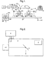
- the radiation system may include a source LA (e.g. an Hg lamp, an excimer laser, a laser-produced plasma source, a discharge plasma source or an undulator or wiggler provided around the path of an electron beam in a storage ring or synchrotron) which produces a beam of UV or EUV radiation.
- a source LA e.g. an Hg lamp, an excimer laser, a laser-produced plasma source, a discharge plasma source or an undulator or wiggler provided around the path of an electron beam in a storage ring or synchrotron
- This beam is caused to traverse various optical components comprised in the illumination system IL - e.g. beam shaping optics, an integrator and a condenser - also included in the radiation system so that the resultant beam PB has a desired shape and intensity distribution in its cross-section.
Landscapes
- Health & Medical Sciences (AREA)
- Epidemiology (AREA)
- Public Health (AREA)
- Physics & Mathematics (AREA)
- Engineering & Computer Science (AREA)
- General Physics & Mathematics (AREA)
- Environmental & Geological Engineering (AREA)
- Atmospheric Sciences (AREA)
- Life Sciences & Earth Sciences (AREA)
- Toxicology (AREA)
- Plasma & Fusion (AREA)
- Exposure And Positioning Against Photoresist Photosensitive Materials (AREA)
- Exposure Of Semiconductors, Excluding Electron Or Ion Beam Exposure (AREA)
- Lenses (AREA)
- Cleaning Or Drying Semiconductors (AREA)
Abstract
Description
- a radiation system for supplying a projection beam of electromagnetic radiation having a wavelength of 250nm or less;
- a support structure for supporting patterning means, the patterning means serving to pattern the projection beam according to a desired pattern;
- a substrate table for holding a substrate; and
- a projection system for projecting the patterned beam onto a target portion of the substrate.
- A mask. The concept of a mask is well known in lithography, and it includes mask types such as binary, alternating phase-shift, and attenuated phase-shift, as well as various hybrid mask types. Placement of such a mask in the radiation beam causes selective transmission (in the case of a transmissive mask) or reflection (in the case of a reflective mask) of the radiation impinging on the mask, according to the pattern on the mask. In the case of a mask, the support structure will generally be a mask table, which ensures that the mask can be held at a desired position in the incoming radiation beam, and that it can be moved relative to the beam if so desired.
- A programmable mirror array. An example of such a device is a matrix-addressable surface having a viscoelastic control layer and a reflective surface. The basic principle behind such an apparatus is that (for example) addressed areas of the reflective surface reflect incident light as diffracted light, whereas unaddressed areas reflect incident light as undiffracted light. Using an appropriate filter, the said undiffracted light can be filtered out of the reflected beam, leaving only the diffracted light behind; in this manner, the beam becomes patterned according to the addressing pattern of the matrix-adressable surface. The required matrix addressing can be performed using suitable electronic means. More information on such mirror arrays can be gleaned, for example, from US 5,296,891 and US 5,523,193, which are incorporated herein by reference. In the case of a programmable mirror array, the said support structure may be embodied as a frame or table, for example, which may be fixed or movable as required.
- A programmable LCD array. An example of such a construction is given in US 5,229,872, which is incorporated herein by reference. As above, the support structure in this case may be embodied as a frame or table, for example, which may be fixed or movable as required.
Contaminant particles such as hydrocarbon molecules and water vapor may be introduced into the system from external sources, or they may be generated within the lithographic apparatus itself. For example the contaminant particles may include the debris and by-products that are liberated from the substrate, for example by an EUV radiation beam, or molecules produced through evaporation of plastics, adhesives and lubricants used in the apparatus.
Claims (8)
- A lithographic projection apparatus comprising:a radiation system for supplying a projection beam of electromagnetic radiation having a wavelength of 250nm or less;a support structure for supporting patterning means, the patterning means serving to pattern the projection beam according to a desired pattern;a substrate table for holding a substrate;a projection system for projecting the patterned beam onto a target portion of the substrate; anda gas supply for supplying a purge gas to a space in said apparatus, said space containing an optical component positioned to interact with the projection beam, wherein said purge gas comprises molecular oxygen at a total partial pressure of from 1x10⁻⁴ Pa to 1 Pa.
- An apparatus according to claim 1, wherein said purge gas further comprises an inert gas, preferably helium, argon, nitrogen or mixtures thereof, and wherein the total amount of molecular oxygen present in said purge gas is from 1 ppb to 10 ppm by volume.
- An apparatus according to claim 1, wherein said space is substantially evacuated.
- An apparatus according to claim 1, which apparatus further comprises a further supply of electromagnetic radiation having a wavelength of 250nm or less and arranged to supply such radiation onto said optical component.
- A device manufacturing method comprising the steps of:providing a substrate that is at least partially covered by a layer of radiation-sensitive material;providing a projection beam of electromagnetic radiation having a wavelength of 250nm or less;using patterning means to endow the projection beam with a pattern in its cross-section;projecting the patterned beam of radiation onto a target portion of the layer of radiation-sensitive material, andcleaning an optical component for use in the apparatus by irradiating a space containing said optical component which is positioned to interact with the projection beam with the said projection beam and supplying to said space a purge gas comprising molecular oxygen at a total partial pressure of from 1x10⁻⁴ Pa to 1 Pa..
- A method according to claim 5, wherein the purge gas further comprises an inert gas, preferably helium, argon, nitrogen or mixtures thereof, and wherein the total amount of molecular oxygen present in said purge gas is from 1 ppb to 10 ppm by volume.
- A method according to claim 5, wherein said space is substantially evacuated.
- A method according to claim 5, further comprising the steps of:supplying a further beam of electromagnetic radiation having a wavelength of 250nm or less, andirradiating said optical component with said further beam of electromagnetic radiation, while projecting said patterned beam of radiation onto said target portion.
Applications Claiming Priority (2)
| Application Number | Priority Date | Filing Date | Title |
|---|---|---|---|
| US09/988,391 US6828569B2 (en) | 2001-11-19 | 2001-11-19 | Lithographic projection apparatus, device manufacturing method and device manufactured thereby |
| US988391 | 2001-11-19 |
Publications (3)
| Publication Number | Publication Date |
|---|---|
| EP1312984A2 true EP1312984A2 (en) | 2003-05-21 |
| EP1312984A3 EP1312984A3 (en) | 2005-05-25 |
| EP1312984B1 EP1312984B1 (en) | 2007-03-14 |
Family
ID=25534075
Family Applications (1)
| Application Number | Title | Priority Date | Filing Date |
|---|---|---|---|
| EP02257914A Expired - Lifetime EP1312984B1 (en) | 2001-11-19 | 2002-11-15 | Device manufacturing method |
Country Status (8)
| Country | Link |
|---|---|
| US (2) | US6828569B2 (en) |
| EP (1) | EP1312984B1 (en) |
| JP (1) | JP4194831B2 (en) |
| KR (1) | KR100767829B1 (en) |
| CN (1) | CN1322545C (en) |
| DE (1) | DE60218802T2 (en) |
| SG (1) | SG120897A1 (en) |
| TW (1) | TWI266960B (en) |
Cited By (1)
| Publication number | Priority date | Publication date | Assignee | Title |
|---|---|---|---|---|
| US7476491B2 (en) | 2004-09-15 | 2009-01-13 | Asml Netherlands B.V. | Lithographic apparatus, gas supply system, method for purging, and device manufacturing method and device manufactured thereby |
Families Citing this family (31)
| Publication number | Priority date | Publication date | Assignee | Title |
|---|---|---|---|---|
| DE10209493B4 (en) * | 2002-03-07 | 2007-03-22 | Carl Zeiss Smt Ag | Method for avoiding contamination on optical elements, device for controlling contamination on optical elements and EUV lithography device |
| US20050229947A1 (en) * | 2002-06-14 | 2005-10-20 | Mykrolis Corporation | Methods of inserting or removing a species from a substrate |
| ITTO20020787A1 (en) * | 2002-09-10 | 2004-03-11 | St Microelectronics Srl | PERFECTED, RELATIVE IONIC IMPLANTATION MACHINE |
| US7189291B2 (en) * | 2003-06-02 | 2007-03-13 | Entegris, Inc. | Method for the removal of airborne molecular contaminants using oxygen gas mixtures |
| US7384149B2 (en) * | 2003-07-21 | 2008-06-10 | Asml Netherlands B.V. | Lithographic projection apparatus, gas purging method and device manufacturing method and purge gas supply system |
| US20060285091A1 (en) * | 2003-07-21 | 2006-12-21 | Parekh Bipin S | Lithographic projection apparatus, gas purging method, device manufacturing method and purge gas supply system related application |
| US20060119811A1 (en) * | 2004-12-07 | 2006-06-08 | Asml Netherlands B.V. | Radiation exposure apparatus comprising a gas flushing system |
| CN101095084A (en) * | 2004-12-14 | 2007-12-26 | 拉多韦有限公司 | Process and apparatus for the production of collimated uv rays for photolithographic transfer |
| DE102005031792A1 (en) * | 2005-07-07 | 2007-01-11 | Carl Zeiss Smt Ag | Method for removing contamination of optical elements, in particular surfaces of optical elements, and an optical system or subsystem therefor |
| JP2009503899A (en) * | 2005-08-03 | 2009-01-29 | インテグリス・インコーポレーテッド | Transfer container |
| US7986395B2 (en) * | 2005-10-24 | 2011-07-26 | Taiwan Semiconductor Manufacturing Company, Ltd. | Immersion lithography apparatus and methods |
| KR100739424B1 (en) * | 2005-10-28 | 2007-07-13 | 삼성전기주식회사 | Manufacturing method of exposure apparatus and printed circuit board using inert gas injection |
| US7405417B2 (en) * | 2005-12-20 | 2008-07-29 | Asml Netherlands B.V. | Lithographic apparatus having a monitoring device for detecting contamination |
| US20070284541A1 (en) * | 2006-06-08 | 2007-12-13 | Vane Ronald A | Oxidative cleaning method and apparatus for electron microscopes using UV excitation in a oxygen radical source |
| US8507879B2 (en) * | 2006-06-08 | 2013-08-13 | Xei Scientific, Inc. | Oxidative cleaning method and apparatus for electron microscopes using UV excitation in an oxygen radical source |
| US8564759B2 (en) * | 2006-06-29 | 2013-10-22 | Taiwan Semiconductor Manufacturing Company, Ltd. | Apparatus and method for immersion lithography |
| JP4802937B2 (en) * | 2006-08-24 | 2011-10-26 | 大日本印刷株式会社 | Photomask cleaning method |
| KR100817066B1 (en) * | 2006-10-11 | 2008-03-27 | 삼성전자주식회사 | Ultraviolet-ray exposure apparatus capable of performing substrate exposure and optical element cleaning in situ and method for cleaning optical element included therein |
| JP2008277585A (en) * | 2007-04-27 | 2008-11-13 | Canon Inc | Exposure apparatus cleaning apparatus and exposure apparatus |
| NL1036769A1 (en) * | 2008-04-23 | 2009-10-26 | Asml Netherlands Bv | Lithographic apparatus, device manufacturing method, cleaning system and method for cleaning a patterning device. |
| US8394203B2 (en) * | 2008-10-02 | 2013-03-12 | Molecular Imprints, Inc. | In-situ cleaning of an imprint lithography tool |
| DE102009045008A1 (en) * | 2008-10-15 | 2010-04-29 | Carl Zeiss Smt Ag | EUV lithography apparatus and method for processing a mask |
| US8633459B2 (en) * | 2011-03-02 | 2014-01-21 | Cymer, Llc | Systems and methods for optics cleaning in an EUV light source |
| JP2013080810A (en) * | 2011-10-04 | 2013-05-02 | Lasertec Corp | Euv mask inspection device and euv mask inspection method |
| JP6034598B2 (en) * | 2012-05-31 | 2016-11-30 | ギガフォトン株式会社 | Cleaning method for EUV light generation apparatus |
| KR102427325B1 (en) | 2015-06-03 | 2022-08-01 | 삼성전자주식회사 | Apparatus for lithograpy and method for cleaning of the same |
| DE102016216266A1 (en) | 2016-08-30 | 2017-08-31 | Carl Zeiss Smt Gmbh | Apparatus and method for cleaning an object |
| DE102017114216A1 (en) * | 2017-06-27 | 2018-04-19 | Asml Netherlands B.V. | Arrangement for reducing contamination in an optical system, in particular in a microlithographic projection exposure apparatus |
| CN112204472B (en) * | 2018-05-28 | 2024-10-11 | Asml荷兰有限公司 | Lithography equipment |
| CN114072732A (en) * | 2019-07-01 | 2022-02-18 | Asml荷兰有限公司 | Surface treatment apparatus and method for surface treating patterning devices and other substrates |
| CN113031391B (en) * | 2021-03-05 | 2023-06-30 | 中国科学院光电技术研究所 | Simple ultraviolet nanoimprint lithography device |
Family Cites Families (16)
| Publication number | Priority date | Publication date | Assignee | Title |
|---|---|---|---|---|
| US5099557A (en) * | 1988-07-08 | 1992-03-31 | Engelsberg Audrey C | Removal of surface contaminants by irradiation from a high-energy source |
| US5559584A (en) * | 1993-03-08 | 1996-09-24 | Nikon Corporation | Exposure apparatus |
| BE1007907A3 (en) | 1993-12-24 | 1995-11-14 | Asm Lithography Bv | LENS SYSTEM WITH HOLDER MADE IN gasfilled lens elements and photolithographic DEVICE WITH SUCH A SYSTEM. |
| US6268904B1 (en) * | 1997-04-23 | 2001-07-31 | Nikon Corporation | Optical exposure apparatus and photo-cleaning method |
| EP0997761A4 (en) * | 1997-06-10 | 2000-09-13 | Nippon Kogaku Kk | Optical device, method of cleaning the same, projection aligner, and method of producing the same |
| JPH1116802A (en) * | 1997-06-19 | 1999-01-22 | Toshiba Corp | Exposure method and exposure apparatus |
| US6014398A (en) * | 1997-10-10 | 2000-01-11 | Cymer, Inc. | Narrow band excimer laser with gas additive |
| WO1999005708A1 (en) | 1997-07-22 | 1999-02-04 | Nikon Corporation | Projection exposure method, projection aligner, and methods of manufacturing and optically cleaning the aligner |
| JPH11224839A (en) * | 1998-02-04 | 1999-08-17 | Canon Inc | Exposure apparatus, device manufacturing method, and optical element cleaning method of the exposure apparatus |
| AU1801700A (en) * | 1998-12-28 | 2000-07-24 | Nikon Corporation | Method for cleaning optical device, exposure apparatus and exposure method, method for manufacturing device, and device |
| US6394109B1 (en) * | 1999-04-13 | 2002-05-28 | Applied Materials, Inc. | Method and apparatus for removing carbon contamination in a sub-atmospheric charged particle beam lithography system |
| US6387602B1 (en) * | 2000-02-15 | 2002-05-14 | Silicon Valley Group, Inc. | Apparatus and method of cleaning reticles for use in a lithography tool |
| US6571057B2 (en) * | 2000-03-27 | 2003-05-27 | Nikon Corporation | Optical instrument, gas replacement method and cleaning method of optical instrument, exposure apparatus, exposure method and manufacturing method for devices |
| JP2001293442A (en) * | 2000-04-17 | 2001-10-23 | Canon Inc | Optical element cleaning method |
| US6724460B2 (en) * | 2001-11-19 | 2004-04-20 | Asml Netherlands B.V. | Lithographic projection apparatus, device manufacturing method, device manufactured thereby, cleaning unit and method of cleaning contaminated objects |
| KR100772125B1 (en) * | 2002-06-26 | 2007-10-31 | 이유브이 리미티드 라이어빌러티 코포레이션 | Process to reduce spin-infused surface contamination |
-
2001
- 2001-11-19 US US09/988,391 patent/US6828569B2/en not_active Expired - Lifetime
-
2002
- 2002-11-15 JP JP2002369012A patent/JP4194831B2/en not_active Expired - Fee Related
- 2002-11-15 KR KR1020020071225A patent/KR100767829B1/en not_active Expired - Fee Related
- 2002-11-15 SG SG200206978A patent/SG120897A1/en unknown
- 2002-11-15 EP EP02257914A patent/EP1312984B1/en not_active Expired - Lifetime
- 2002-11-15 DE DE60218802T patent/DE60218802T2/en not_active Expired - Fee Related
- 2002-11-15 TW TW091133501A patent/TWI266960B/en not_active IP Right Cessation
- 2002-11-15 CN CNB021518726A patent/CN1322545C/en not_active Expired - Lifetime
-
2004
- 2004-10-27 US US10/973,250 patent/US7115886B2/en not_active Expired - Lifetime
Cited By (1)
| Publication number | Priority date | Publication date | Assignee | Title |
|---|---|---|---|---|
| US7476491B2 (en) | 2004-09-15 | 2009-01-13 | Asml Netherlands B.V. | Lithographic apparatus, gas supply system, method for purging, and device manufacturing method and device manufactured thereby |
Also Published As
| Publication number | Publication date |
|---|---|
| TW200407680A (en) | 2004-05-16 |
| US6828569B2 (en) | 2004-12-07 |
| JP4194831B2 (en) | 2008-12-10 |
| CN1322545C (en) | 2007-06-20 |
| CN1474234A (en) | 2004-02-11 |
| KR20030075136A (en) | 2003-09-22 |
| EP1312984B1 (en) | 2007-03-14 |
| DE60218802D1 (en) | 2007-04-26 |
| US20050112508A1 (en) | 2005-05-26 |
| JP2003234287A (en) | 2003-08-22 |
| US20030096193A1 (en) | 2003-05-22 |
| DE60218802T2 (en) | 2007-12-06 |
| US7115886B2 (en) | 2006-10-03 |
| KR100767829B1 (en) | 2007-10-17 |
| SG120897A1 (en) | 2006-04-26 |
| TWI266960B (en) | 2006-11-21 |
| EP1312984A3 (en) | 2005-05-25 |
Similar Documents
| Publication | Publication Date | Title |
|---|---|---|
| EP1312984B1 (en) | Device manufacturing method | |
| EP1312983B1 (en) | Photocleaning | |
| US7450215B2 (en) | Lithographic projection apparatus, gas purging method, device manufacturing method and purge gas supply system | |
| US7315346B2 (en) | Lithographic apparatus and device manufacturing method | |
| US7230674B2 (en) | Lithographic apparatus and device manufacturing method | |
| EP1429189B1 (en) | Lithographic apparatus and device manufacturing method | |
| US7476491B2 (en) | Lithographic apparatus, gas supply system, method for purging, and device manufacturing method and device manufactured thereby | |
| JP4429201B2 (en) | Lithographic apparatus and device manufacturing method | |
| US6714279B2 (en) | Lithographic projection apparatus, device manufacturing method and device manufactured thereby | |
| EP1186958B1 (en) | Lithographic projection apparatus | |
| EP1403715A2 (en) | Lithographic apparatus and device manufacturing method | |
| US20110149256A1 (en) | Object with an improved suitability for a plasma cleaning treatment | |
| WO2008150167A1 (en) | Extreme ultra-violet lithographic apparatus and device manufacturing method | |
| EP1528434A1 (en) | Lithographic apparatus and device manufacturing method |
Legal Events
| Date | Code | Title | Description |
|---|---|---|---|
| PUAI | Public reference made under article 153(3) epc to a published international application that has entered the european phase |
Free format text: ORIGINAL CODE: 0009012 |
|
| AK | Designated contracting states |
Designated state(s): AT BE BG CH CY CZ DE DK EE ES FI FR GB GR IE IT LI LU MC NL PT SE SK TR |
|
| AX | Request for extension of the european patent |
Extension state: AL LT LV MK RO SI |
|
| RAP1 | Party data changed (applicant data changed or rights of an application transferred) |
Owner name: ASML NETHERLANDS B.V. |
|
| PUAL | Search report despatched |
Free format text: ORIGINAL CODE: 0009013 |
|
| AK | Designated contracting states |
Kind code of ref document: A3 Designated state(s): AT BE BG CH CY CZ DE DK EE ES FI FR GB GR IE IT LI LU MC NL PT SE SK TR |
|
| AX | Request for extension of the european patent |
Extension state: AL LT LV MK RO SI |
|
| 17P | Request for examination filed |
Effective date: 20050628 |
|
| AKX | Designation fees paid |
Designated state(s): DE FR GB IT NL |
|
| GRAP | Despatch of communication of intention to grant a patent |
Free format text: ORIGINAL CODE: EPIDOSNIGR1 |
|
| RTI1 | Title (correction) |
Free format text: DEVICE MANUFACTURING METHOD |
|
| GRAS | Grant fee paid |
Free format text: ORIGINAL CODE: EPIDOSNIGR3 |
|
| GRAA | (expected) grant |
Free format text: ORIGINAL CODE: 0009210 |
|
| AK | Designated contracting states |
Kind code of ref document: B1 Designated state(s): DE FR GB IT NL |
|
| REG | Reference to a national code |
Ref country code: GB Ref legal event code: FG4D |
|
| REF | Corresponds to: |
Ref document number: 60218802 Country of ref document: DE Date of ref document: 20070426 Kind code of ref document: P |
|
| PLBE | No opposition filed within time limit |
Free format text: ORIGINAL CODE: 0009261 |
|
| STAA | Information on the status of an ep patent application or granted ep patent |
Free format text: STATUS: NO OPPOSITION FILED WITHIN TIME LIMIT |
|
| 26N | No opposition filed |
Effective date: 20071217 |
|
| PGFP | Annual fee paid to national office [announced via postgrant information from national office to epo] |
Ref country code: DE Payment date: 20081121 Year of fee payment: 7 Ref country code: NL Payment date: 20081113 Year of fee payment: 7 |
|
| PGFP | Annual fee paid to national office [announced via postgrant information from national office to epo] |
Ref country code: IT Payment date: 20081120 Year of fee payment: 7 |
|
| PGFP | Annual fee paid to national office [announced via postgrant information from national office to epo] |
Ref country code: FR Payment date: 20081113 Year of fee payment: 7 |
|
| PGFP | Annual fee paid to national office [announced via postgrant information from national office to epo] |
Ref country code: GB Payment date: 20081117 Year of fee payment: 7 |
|
| REG | Reference to a national code |
Ref country code: NL Ref legal event code: V1 Effective date: 20100601 |
|
| GBPC | Gb: european patent ceased through non-payment of renewal fee |
Effective date: 20091115 |
|
| REG | Reference to a national code |
Ref country code: FR Ref legal event code: ST Effective date: 20100730 |
|
| PG25 | Lapsed in a contracting state [announced via postgrant information from national office to epo] |
Ref country code: FR Free format text: LAPSE BECAUSE OF NON-PAYMENT OF DUE FEES Effective date: 20091130 Ref country code: NL Free format text: LAPSE BECAUSE OF NON-PAYMENT OF DUE FEES Effective date: 20100601 |
|
| PG25 | Lapsed in a contracting state [announced via postgrant information from national office to epo] |
Ref country code: DE Free format text: LAPSE BECAUSE OF NON-PAYMENT OF DUE FEES Effective date: 20100601 |
|
| PG25 | Lapsed in a contracting state [announced via postgrant information from national office to epo] |
Ref country code: GB Free format text: LAPSE BECAUSE OF NON-PAYMENT OF DUE FEES Effective date: 20091115 |
|
| PG25 | Lapsed in a contracting state [announced via postgrant information from national office to epo] |
Ref country code: IT Free format text: LAPSE BECAUSE OF NON-PAYMENT OF DUE FEES Effective date: 20091115 |