EP1311072A1 - Transmitter and receiver module - Google Patents
Transmitter and receiver module Download PDFInfo
- Publication number
- EP1311072A1 EP1311072A1 EP00953467A EP00953467A EP1311072A1 EP 1311072 A1 EP1311072 A1 EP 1311072A1 EP 00953467 A EP00953467 A EP 00953467A EP 00953467 A EP00953467 A EP 00953467A EP 1311072 A1 EP1311072 A1 EP 1311072A1
- Authority
- EP
- European Patent Office
- Prior art keywords
- package
- transmitter
- partial
- electronic components
- millimeter wave
- Prior art date
- Legal status (The legal status is an assumption and is not a legal conclusion. Google has not performed a legal analysis and makes no representation as to the accuracy of the status listed.)
- Withdrawn
Links
Images


Classifications
-
- G—PHYSICS
- G01—MEASURING; TESTING
- G01S—RADIO DIRECTION-FINDING; RADIO NAVIGATION; DETERMINING DISTANCE OR VELOCITY BY USE OF RADIO WAVES; LOCATING OR PRESENCE-DETECTING BY USE OF THE REFLECTION OR RERADIATION OF RADIO WAVES; ANALOGOUS ARRANGEMENTS USING OTHER WAVES
- G01S7/00—Details of systems according to groups G01S13/00, G01S15/00, G01S17/00
- G01S7/02—Details of systems according to groups G01S13/00, G01S15/00, G01S17/00 of systems according to group G01S13/00
- G01S7/03—Details of HF subsystems specially adapted therefor, e.g. common to transmitter and receiver
- G01S7/032—Constructional details for solid-state radar subsystems
-
- G—PHYSICS
- G01—MEASURING; TESTING
- G01S—RADIO DIRECTION-FINDING; RADIO NAVIGATION; DETERMINING DISTANCE OR VELOCITY BY USE OF RADIO WAVES; LOCATING OR PRESENCE-DETECTING BY USE OF THE REFLECTION OR RERADIATION OF RADIO WAVES; ANALOGOUS ARRANGEMENTS USING OTHER WAVES
- G01S13/00—Systems using the reflection or reradiation of radio waves, e.g. radar systems; Analogous systems using reflection or reradiation of waves whose nature or wavelength is irrelevant or unspecified
- G01S13/88—Radar or analogous systems specially adapted for specific applications
- G01S13/93—Radar or analogous systems specially adapted for specific applications for anti-collision purposes
- G01S13/931—Radar or analogous systems specially adapted for specific applications for anti-collision purposes of land vehicles
-
- H—ELECTRICITY
- H01—ELECTRIC ELEMENTS
- H01Q—ANTENNAS, i.e. RADIO AERIALS
- H01Q1/00—Details of, or arrangements associated with, antennas
- H01Q1/42—Housings not intimately mechanically associated with radiating elements, e.g. radome
-
- H—ELECTRICITY
- H01—ELECTRIC ELEMENTS
- H01Q—ANTENNAS, i.e. RADIO AERIALS
- H01Q23/00—Antennas with active circuits or circuit elements integrated within them or attached to them
-
- H—ELECTRICITY
- H04—ELECTRIC COMMUNICATION TECHNIQUE
- H04B—TRANSMISSION
- H04B1/00—Details of transmission systems, not covered by a single one of groups H04B3/00 - H04B13/00; Details of transmission systems not characterised by the medium used for transmission
- H04B1/38—Transceivers, i.e. devices in which transmitter and receiver form a structural unit and in which at least one part is used for functions of transmitting and receiving
-
- H—ELECTRICITY
- H10—SEMICONDUCTOR DEVICES; ELECTRIC SOLID-STATE DEVICES NOT OTHERWISE PROVIDED FOR
- H10W—GENERIC PACKAGES, INTERCONNECTIONS, CONNECTORS OR OTHER CONSTRUCTIONAL DETAILS OF DEVICES COVERED BY CLASS H10
- H10W74/00—Encapsulations, e.g. protective coatings
- H10W74/10—Encapsulations, e.g. protective coatings characterised by their shape or disposition
- H10W74/111—Encapsulations, e.g. protective coatings characterised by their shape or disposition the semiconductor body being completely enclosed
- H10W74/121—Encapsulations, e.g. protective coatings characterised by their shape or disposition the semiconductor body being completely enclosed by multiple encapsulations, e.g. by a thin protective coating and a thick encapsulation
-
- H—ELECTRICITY
- H10—SEMICONDUCTOR DEVICES; ELECTRIC SOLID-STATE DEVICES NOT OTHERWISE PROVIDED FOR
- H10W—GENERIC PACKAGES, INTERCONNECTIONS, CONNECTORS OR OTHER CONSTRUCTIONAL DETAILS OF DEVICES COVERED BY CLASS H10
- H10W76/00—Containers; Fillings or auxiliary members therefor; Seals
- H10W76/10—Containers or parts thereof
- H10W76/12—Containers or parts thereof characterised by their shape
- H10W76/13—Containers comprising a conductive base serving as an interconnection
- H10W76/132—Containers comprising a conductive base serving as an interconnection having other interconnections through an insulated passage in the conductive base
-
- H—ELECTRICITY
- H10—SEMICONDUCTOR DEVICES; ELECTRIC SOLID-STATE DEVICES NOT OTHERWISE PROVIDED FOR
- H10W—GENERIC PACKAGES, INTERCONNECTIONS, CONNECTORS OR OTHER CONSTRUCTIONAL DETAILS OF DEVICES COVERED BY CLASS H10
- H10W76/00—Containers; Fillings or auxiliary members therefor; Seals
- H10W76/10—Containers or parts thereof
- H10W76/12—Containers or parts thereof characterised by their shape
- H10W76/15—Containers comprising an insulating or insulated base
- H10W76/153—Containers comprising an insulating or insulated base having interconnections in passages through the insulating or insulated base
-
- H—ELECTRICITY
- H10—SEMICONDUCTOR DEVICES; ELECTRIC SOLID-STATE DEVICES NOT OTHERWISE PROVIDED FOR
- H10W—GENERIC PACKAGES, INTERCONNECTIONS, CONNECTORS OR OTHER CONSTRUCTIONAL DETAILS OF DEVICES COVERED BY CLASS H10
- H10W76/00—Containers; Fillings or auxiliary members therefor; Seals
- H10W76/60—Seals
-
- H—ELECTRICITY
- H10—SEMICONDUCTOR DEVICES; ELECTRIC SOLID-STATE DEVICES NOT OTHERWISE PROVIDED FOR
- H10W—GENERIC PACKAGES, INTERCONNECTIONS, CONNECTORS OR OTHER CONSTRUCTIONAL DETAILS OF DEVICES COVERED BY CLASS H10
- H10W90/00—Package configurations
-
- G—PHYSICS
- G01—MEASURING; TESTING
- G01S—RADIO DIRECTION-FINDING; RADIO NAVIGATION; DETERMINING DISTANCE OR VELOCITY BY USE OF RADIO WAVES; LOCATING OR PRESENCE-DETECTING BY USE OF THE REFLECTION OR RERADIATION OF RADIO WAVES; ANALOGOUS ARRANGEMENTS USING OTHER WAVES
- G01S13/00—Systems using the reflection or reradiation of radio waves, e.g. radar systems; Analogous systems using reflection or reradiation of waves whose nature or wavelength is irrelevant or unspecified
- G01S13/88—Radar or analogous systems specially adapted for specific applications
- G01S13/93—Radar or analogous systems specially adapted for specific applications for anti-collision purposes
- G01S13/931—Radar or analogous systems specially adapted for specific applications for anti-collision purposes of land vehicles
- G01S2013/9321—Velocity regulation, e.g. cruise control
-
- G—PHYSICS
- G01—MEASURING; TESTING
- G01S—RADIO DIRECTION-FINDING; RADIO NAVIGATION; DETERMINING DISTANCE OR VELOCITY BY USE OF RADIO WAVES; LOCATING OR PRESENCE-DETECTING BY USE OF THE REFLECTION OR RERADIATION OF RADIO WAVES; ANALOGOUS ARRANGEMENTS USING OTHER WAVES
- G01S13/00—Systems using the reflection or reradiation of radio waves, e.g. radar systems; Analogous systems using reflection or reradiation of waves whose nature or wavelength is irrelevant or unspecified
- G01S13/88—Radar or analogous systems specially adapted for specific applications
- G01S13/93—Radar or analogous systems specially adapted for specific applications for anti-collision purposes
- G01S13/931—Radar or analogous systems specially adapted for specific applications for anti-collision purposes of land vehicles
- G01S2013/9325—Radar or analogous systems specially adapted for specific applications for anti-collision purposes of land vehicles for inter-vehicle distance regulation, e.g. navigating in platoons
-
- H—ELECTRICITY
- H05—ELECTRIC TECHNIQUES NOT OTHERWISE PROVIDED FOR
- H05K—PRINTED CIRCUITS; CASINGS OR CONSTRUCTIONAL DETAILS OF ELECTRIC APPARATUS; MANUFACTURE OF ASSEMBLAGES OF ELECTRICAL COMPONENTS
- H05K1/00—Printed circuits
- H05K1/02—Details
- H05K1/14—Structural association of two or more printed circuits
- H05K1/141—One or more single auxiliary printed circuits mounted on a main printed circuit, e.g. modules, adapters
-
- H—ELECTRICITY
- H05—ELECTRIC TECHNIQUES NOT OTHERWISE PROVIDED FOR
- H05K—PRINTED CIRCUITS; CASINGS OR CONSTRUCTIONAL DETAILS OF ELECTRIC APPARATUS; MANUFACTURE OF ASSEMBLAGES OF ELECTRICAL COMPONENTS
- H05K3/00—Apparatus or processes for manufacturing printed circuits
- H05K3/22—Secondary treatment of printed circuits
- H05K3/28—Applying non-metallic protective coatings
- H05K3/284—Applying non-metallic protective coatings for encapsulating mounted components
-
- H—ELECTRICITY
- H10—SEMICONDUCTOR DEVICES; ELECTRIC SOLID-STATE DEVICES NOT OTHERWISE PROVIDED FOR
- H10W—GENERIC PACKAGES, INTERCONNECTIONS, CONNECTORS OR OTHER CONSTRUCTIONAL DETAILS OF DEVICES COVERED BY CLASS H10
- H10W44/00—Electrical arrangements for controlling or matching impedance
- H10W44/20—Electrical arrangements for controlling or matching impedance at high-frequency [HF] or radio frequency [RF]
- H10W44/241—Electrical arrangements for controlling or matching impedance at high-frequency [HF] or radio frequency [RF] for passive devices or passive elements
- H10W44/248—Electrical arrangements for controlling or matching impedance at high-frequency [HF] or radio frequency [RF] for passive devices or passive elements for antennas
-
- H—ELECTRICITY
- H10—SEMICONDUCTOR DEVICES; ELECTRIC SOLID-STATE DEVICES NOT OTHERWISE PROVIDED FOR
- H10W—GENERIC PACKAGES, INTERCONNECTIONS, CONNECTORS OR OTHER CONSTRUCTIONAL DETAILS OF DEVICES COVERED BY CLASS H10
- H10W72/00—Interconnections or connectors in packages
- H10W72/071—Connecting or disconnecting
- H10W72/075—Connecting or disconnecting of bond wires
-
- H—ELECTRICITY
- H10—SEMICONDUCTOR DEVICES; ELECTRIC SOLID-STATE DEVICES NOT OTHERWISE PROVIDED FOR
- H10W—GENERIC PACKAGES, INTERCONNECTIONS, CONNECTORS OR OTHER CONSTRUCTIONAL DETAILS OF DEVICES COVERED BY CLASS H10
- H10W72/00—Interconnections or connectors in packages
- H10W72/50—Bond wires
- H10W72/541—Dispositions of bond wires
- H10W72/5445—Dispositions of bond wires being orthogonal to a side surface of the chip, e.g. parallel arrangements
-
- H—ELECTRICITY
- H10—SEMICONDUCTOR DEVICES; ELECTRIC SOLID-STATE DEVICES NOT OTHERWISE PROVIDED FOR
- H10W—GENERIC PACKAGES, INTERCONNECTIONS, CONNECTORS OR OTHER CONSTRUCTIONAL DETAILS OF DEVICES COVERED BY CLASS H10
- H10W72/00—Interconnections or connectors in packages
- H10W72/50—Bond wires
- H10W72/551—Materials of bond wires
-
- H—ELECTRICITY
- H10—SEMICONDUCTOR DEVICES; ELECTRIC SOLID-STATE DEVICES NOT OTHERWISE PROVIDED FOR
- H10W—GENERIC PACKAGES, INTERCONNECTIONS, CONNECTORS OR OTHER CONSTRUCTIONAL DETAILS OF DEVICES COVERED BY CLASS H10
- H10W72/00—Interconnections or connectors in packages
- H10W72/851—Dispositions of multiple connectors or interconnections
- H10W72/874—On different surfaces
- H10W72/884—Die-attach connectors and bond wires
-
- H—ELECTRICITY
- H10—SEMICONDUCTOR DEVICES; ELECTRIC SOLID-STATE DEVICES NOT OTHERWISE PROVIDED FOR
- H10W—GENERIC PACKAGES, INTERCONNECTIONS, CONNECTORS OR OTHER CONSTRUCTIONAL DETAILS OF DEVICES COVERED BY CLASS H10
- H10W72/00—Interconnections or connectors in packages
- H10W72/90—Bond pads, in general
- H10W72/931—Shapes of bond pads
- H10W72/932—Plan-view shape, i.e. in top view
-
- H—ELECTRICITY
- H10—SEMICONDUCTOR DEVICES; ELECTRIC SOLID-STATE DEVICES NOT OTHERWISE PROVIDED FOR
- H10W—GENERIC PACKAGES, INTERCONNECTIONS, CONNECTORS OR OTHER CONSTRUCTIONAL DETAILS OF DEVICES COVERED BY CLASS H10
- H10W72/00—Interconnections or connectors in packages
- H10W72/90—Bond pads, in general
- H10W72/951—Materials of bond pads
-
- H—ELECTRICITY
- H10—SEMICONDUCTOR DEVICES; ELECTRIC SOLID-STATE DEVICES NOT OTHERWISE PROVIDED FOR
- H10W—GENERIC PACKAGES, INTERCONNECTIONS, CONNECTORS OR OTHER CONSTRUCTIONAL DETAILS OF DEVICES COVERED BY CLASS H10
- H10W74/00—Encapsulations, e.g. protective coatings
-
- H—ELECTRICITY
- H10—SEMICONDUCTOR DEVICES; ELECTRIC SOLID-STATE DEVICES NOT OTHERWISE PROVIDED FOR
- H10W—GENERIC PACKAGES, INTERCONNECTIONS, CONNECTORS OR OTHER CONSTRUCTIONAL DETAILS OF DEVICES COVERED BY CLASS H10
- H10W90/00—Package configurations
- H10W90/701—Package configurations characterised by the relative positions of pads or connectors relative to package parts
- H10W90/721—Package configurations characterised by the relative positions of pads or connectors relative to package parts of bump connectors
- H10W90/724—Package configurations characterised by the relative positions of pads or connectors relative to package parts of bump connectors between a chip and a stacked insulating package substrate, interposer or RDL
-
- H—ELECTRICITY
- H10—SEMICONDUCTOR DEVICES; ELECTRIC SOLID-STATE DEVICES NOT OTHERWISE PROVIDED FOR
- H10W—GENERIC PACKAGES, INTERCONNECTIONS, CONNECTORS OR OTHER CONSTRUCTIONAL DETAILS OF DEVICES COVERED BY CLASS H10
- H10W90/00—Package configurations
- H10W90/701—Package configurations characterised by the relative positions of pads or connectors relative to package parts
- H10W90/731—Package configurations characterised by the relative positions of pads or connectors relative to package parts of die-attach connectors
- H10W90/734—Package configurations characterised by the relative positions of pads or connectors relative to package parts of die-attach connectors between a chip and a stacked insulating package substrate, interposer or RDL
-
- H—ELECTRICITY
- H10—SEMICONDUCTOR DEVICES; ELECTRIC SOLID-STATE DEVICES NOT OTHERWISE PROVIDED FOR
- H10W—GENERIC PACKAGES, INTERCONNECTIONS, CONNECTORS OR OTHER CONSTRUCTIONAL DETAILS OF DEVICES COVERED BY CLASS H10
- H10W90/00—Package configurations
- H10W90/701—Package configurations characterised by the relative positions of pads or connectors relative to package parts
- H10W90/751—Package configurations characterised by the relative positions of pads or connectors relative to package parts of bond wires
- H10W90/753—Package configurations characterised by the relative positions of pads or connectors relative to package parts of bond wires between laterally-adjacent chips
-
- H—ELECTRICITY
- H10—SEMICONDUCTOR DEVICES; ELECTRIC SOLID-STATE DEVICES NOT OTHERWISE PROVIDED FOR
- H10W—GENERIC PACKAGES, INTERCONNECTIONS, CONNECTORS OR OTHER CONSTRUCTIONAL DETAILS OF DEVICES COVERED BY CLASS H10
- H10W90/00—Package configurations
- H10W90/701—Package configurations characterised by the relative positions of pads or connectors relative to package parts
- H10W90/751—Package configurations characterised by the relative positions of pads or connectors relative to package parts of bond wires
- H10W90/754—Package configurations characterised by the relative positions of pads or connectors relative to package parts of bond wires between a chip and a stacked insulating package substrate, interposer or RDL
Definitions
- the present invention relates to a transmitter-receiver module for use on millimeter wave or semi-millimeter wave bands.
- antennas and transmitter-receiver circuits have been integrated into modules to enhance the mounting density of the radar components (references: Japanese Application Patent Laid-Open Publication Nos. Hei 10-79623, Hei 11-4118, and so on).
- the components to be used in such transmitter-receiver circuits especially, oscillators, power amplifiers, frequency converters (down-converters), and the like, are structured as integrated circuits (ICs), and these IC dies, capacitors, and other electronic components are mounted on circuit boards.
- Hermetic sealing is formed in an inert gas atmosphere such as a nitrogen gas atmosphere, and antenna elements, IC dies, capacitors, and other electronic components are protected with a sealing cover, which is then connected to a circuit board or the like by brazing, laser welding, electric welding, or the like.
- inert gas atmosphere such as a nitrogen gas atmosphere
- antenna elements, IC dies, capacitors, and other electronic components are protected with a sealing cover, which is then connected to a circuit board or the like by brazing, laser welding, electric welding, or the like.
- packaging technology suitable for high-frequency signal-use ICs includes independent packaging of each electronic component, such as an IC die, that requires hermetic sealing. It is described in, for example, Japanese Application Patent Laid-Open Publication Nos. Hei 11-251469 and Hei 11-26645, that for high-frequency-use ICs, since the characteristic dielectric constants and loss coefficients of polymer sealing materials cause the losses of gain and output during the propagation of high-frequency signals, the use of IC packages having a cavity inside each are preferable.
- the present invention is based on the situations described above, and its object is to provide a transmitter-receiver module which can be used on millimeter wave and other frequency bands, and which can minimize costs and reduce inspection time with guaranteed measurement reliability.
- the present invention basically proposes the following transmitter-receiver modules:
- One module has partial packages in which only some of the IC dies and other electronic components constituting the transmitter-receiver circuits for use on millimeter wave or semi-millimeter wave bands are to be sealed, and a total package in which all electronic components for the aforementioned transmitter-receiver circuits, including said partial packages, are to be sealed, wherein the module is characterized in that two or more related electronic components are sealed together as a single block in each partial package, in that independent inspection of electrical characteristics is possible for each partial package, and in that either the partial packages or the total package or both are of hermetically sealed structure.
- Another module is such that said partial packages are cavity packages of the structure provided with hermetic sealing or semi-hermetic sealing, such that two or more related electronic components are sealed together as a single block in each partial package, and such that said total package is resin-coated.
- hermetic sealing and “semi-hermetic sealing” here are defined as follows:
- Hermetic structure is structure designed so as to maintain hermetically sealed status during the years of practical use, and applies to, for example, the structure in which the connections that require sealing are connected by brazing or soldering.
- Semi-hermetic structure is structure which, although it can initially maintain the hermeticalness of a practical level, becomes non-hermetic in the long run, and applies to, for example, the structure in which the connections that require sealing are connected using organic adhesive materials or the like.
- a yet another module is such that the IC dies and other electronic components constituting the transmitter-receiver circuits for use on millimeter wave or semi-millimeter wave bands are formed by collectively coating all such components with a resin material of a low dielectric constant and then recoating these components with a general-purpose resin material of a relatively high dielectric constant.
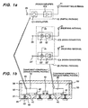
- Fig. 1(a) is a transmitter-receiver module circuit block diagram showing examples of the objects to which the present invention can be applied.
- Fig. 1(b) is a cross-sectinal view of the total package used in the transmitter-receiver module of Fig. 1(a).
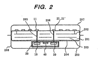
- Fig. 2 is a cross-sectional view showing schematically a millimeter wave radar unit having the above transmitter-receiver module mounted thereon.
- Fig. 3(a) is a profile view showing one partial package of the above transmitter-receiver module, wherein the B-B' section in Fig. 3(b) is cross-sectionally shown.
- Fig. 3 (b) is a cross-sectional view of the A-A' section in Fig. 3(a).
- Fig. 4 is a cross-sectional view of one partial package pertaining to a second embodiment of the present invention.
- Fig. 5 is a cross-sectional view of the partial package 10 pertaining to a third embodiment of the present invention.
- Fig. 6 is a cross-sectional view of the partial package 10 pertaining to a fourth embodiment of the present invention.
- Fig. 7 is a cross-sectional view of the total package 30 pertaining to a fifth embodiment of the present invention.
- Fig. 8 is a cross-sectional view of the transmitter-receiver module pertaining to a sixth embodiment of the present invention.
- Fig. 9 is a cross-sectional view of the transmitter-receiver module pertaining to a seventh embodiment of the present invention.
- Fig. 10 is a cross-sectional view of the transmitter-receiver module pertaining to an eighth embodiment of the present invention.
- the millimeter wave radar unit in a first embodiment is intended to be mounted, for example, in an automobile and applied to vehicle-to-vehicle distance warning and adaptive cruise control (ACC), and the operating frequency assumed is of the order of several tens of gigahertz (GHz).
- ACC vehicle-to-vehicle distance warning and adaptive cruise control
- radio waves of the required millimeter wave band are transmitted from an transmitting antenna 11, then after the waves reflected from a target such as a vehicle have been received at receiving antennas 21 and 21', and the Doppler modulation characteristics of the received waves against the transmitted waves are detected. Thus, the distance and relative speed with respect to the target are detected.
- two receiving antennas (left and right) are used.
- the relative speed and direction angle of the target in front with respect to the radar beam are detected by processing the signals received from both antennas.
- the transmitter in the transmitter-receiver module comprises components such as a semiconductor integrated circuit 1 (IC1) that constitutes an oscillator (for example, a voltage controlled oscillator), and IC2 that constitutes a power amplifier.
- IC1 and IC2 are referred to as oscillation IC1 and power IC2, respectively.
- Oscillation IC1 receives modulation signals from a modulation signal generator (not shown in the figure) via an input terminal 25, and creates millimeter wave signals of the required frequency.
- the receiver in the transmitter-receiver module is equipped with a down-converter (frequency converter) IC3, which performs frequency conversions on the signals received by antenna 21, and a down-converter IC4, which performs frequency conversions on the signals received by antenna 21'.
- the down-converter IC3 comprises a low-noise amplifier 22 and a mixer 23, and the down-converter IC4 comprises a low-noise amplifier 22' and a mixer 23'.
- the mixed signals are sent to a signal processing unit (not shown in the figure) via output terminals 24 and 24', then data concerning both received signals, such as phase differences, is calculated, and finally, the distance and relative speed of the vehicle having the mounted module, with respect to the target, are calculated by a microcomputer.
- the IC1 to the IC4 each consist of an IC die (IC chip).
- the transmitter-receiver module in this embodiment basically consists of partial packages 10 and 20, in which only some of electronic components are to be sealed, and a total package 30, in which all electronic components for the transmitter-receiver circuits, including the partial packages, are to be sealed.
- a plurality of ICs are packaged in the lump for each group whose common electrical characteristics can be inspected on a transmitter-receiver function block unit.
- the oscillation IC1 and power IC2 of the transmitter are contained together in partial package 10.
- the down-converters IC3 and IC4 of the receiver are sealed together in partial package 20.
- these partial packages 10 and 20 are mounted, via solder 42 and together with other related electronic components such as a layered chip capacitor 40, on a circuit board 31 surface-formed with conductor patterns 41.
- the total package 30 consists of a circuit board 31, a casing 32 that forms the receiving space for the components on the circuit board 31, and a sealing cover 33 for covering the casing 32.
- these package components 31, 32 and 33 are formed using a ceramic material.
- Fig. 3 exemplifies the internal structure of the partial package 10.
- the internal structure of the partial package 20 is not described since the package structure is basically the same as that of the partial package 10.
- the partial package 10 is a cavity package composed of a circuit board 101, a casing 102 that forms the receiving space for the components on the circuit board 101, and a sealing cover 103.
- the circuit board 101, the casing 102, and the sealing cover 103 are made of a ceramic material.
- the circuit board 101, the plurality of ceramic terminal blocks 15 arranged on the surface thereof, and the casing 102 are all connected by sintering to form a single block.
- Terminal blocks 15 have an electroconductive film 16 formed on the respective surfaces to function as wire bonding pads (circuit terminals) BP.
- the via-holes running through the terminal blocks 15 and the circuit board 101 are each filled with a conductor 18, through which the wire bonding pads BP and the intermediate terminals IT provided on the reverse side of the circuit board are electrically connected.
- Figs. 3 and 4 six wire bonding pads BP are shown and these pads are represented as BP1 to BP6. Likewise, four intermediate terminals IT are shown and these terminals are represented as IT1 to IT4.
- Oscillation IC1, power IC2, and related single-layer capacitors C1, C2, C3, C4, and C5 are mounted on the circuit board 101 of the partial package 10, and these electronic components are electrically connected via wire bonding 14 and accommodated in package casing 102.
- cover 103 is connected to casing 102 under a nitrogen gas atmosphere to provide the inside of the package with hermetic sealing.
- Cover 103 by being connected to casing 102 by brazing or soldering, maintains the internal hermeticalness of the package, and by being internally charged with an inert gas such as a nitrogen gas, constitutes the cavity package.
- this cavity package enables oscillation ICs, power ICs, down-converter ICs, and the like, to be protected from moisture and thus from deterioration in characteristics, during operation on semi-millimeter wave or millimeter wave bands, in particular.
- Partial packages 10 and 20 and other electronic components are mounted by bonding on the circuit board 31 of the total package 30 via the intermediate terminals IT1 to IT4 provided on the reverse side of the circuit board, and via the solder 42 shown in Fig. 1 (b). Such bonding provides partial packages 10 and 20 with electrical connection to the electroconductive patterns 41 and layered capacitors 40 on circuit board 31.
- Total package 30 by having its cover 33 bonded onto casing 32 via a brazing material or a bonding material 34 such as solder, provides partial packages (IC packages) 10 and 20, other electronic components 40, and the like, with hermetic sealing.
- a brazing material or a bonding material 34 such as solder
- Total package is also a cavity package having a space S2 therein.
- the total package 30 itself is also provided with hermetic sealing, since the components that require hermetic sealing are already hermetically sealed via the partial packages, hermetic structure does not always need to be adopted for the total package and non-hermetic or semi-hermetic structure can also be adopted.
- semi-hermetic structure is structure which, although it can initially maintain the hermeticalness of a practical level, becomes non-hermetic in the long run.
- semi-hermetic structure is to be adopted for the total package, this can be implemented by bonding the casing 32 and the cover 33 by use of an organic adhesive.
- the use of an organic adhesive for achieving hermetic sealing enables cost reduction in comparison to the use of an hermetic bonding material such as a brazing material or solder.
- hermetically sealed structure is adopted for the total package 30, the intended purpose of hermetic sealing can be achieved for partial packages 10 and 20, even if the latter two packages are of semi-hermetic or non-hermetic structure.
- Fig. 2 is a cross-sectional view showing schematically the internal structure where the total package (high-frequency transmitter-receiver module) 30 is further built into a millimeter wave radar module 200.
- the millimeter wave radar module 200 has transmitting-receiving antenna patterns 11, 21, and 21' formed on one side of, for example, a multi-layer ceramic circuit board 201, and a transmitter-receiver module 30 on the other side.
- the transmitting antenna pattern 11 and the power IC output terminals of the partial package 10 are electrically connected via a conductor 205 running through the multi-layer ceramic circuit board 201.
- the receiving antenna pattern 21 and 21' are electrically connected to the signal input terminals of the partial package 20 via a conductor 206 running through the multi-layer ceramic circuit board 201.
- Elements such as an electroconductive film 202 for providing antenna grounding, electroconductive film 203 for supplying power to the transmitter-receiver module, intervene between the layers of the ceramic circuit board 201, and electroconductive patterns 204 are formed on one side of the circuit board 201.
- electroconductive film 202 for providing antenna grounding
- electroconductive film 203 for supplying power to the transmitter-receiver module
- electroconductive patterns 204 are formed on one side of the circuit board 201.
- These millimeter wave radar components are accommodated in a casing 208 and shielded with a redome 207.
- the electrical characteristics of two or more IC dies can be independently inspected on a partial package unit. Although such inspections are performed during defective/nondefective component screening, independent inspection of the partial package 10 is possible by applying test signals (equivalent to frequency modulation signals) to the input terminals provided on the reverse side of the corresponding circuit board 101, and then measuring outputs via the output terminals provided on the reverse side of the package circuit board 101.
- test signals equivalent to frequency modulation signals
- Independent inspection of the partial package 20 is possible by applying test signals (equivalent to receiving antenna signals) to the input terminals provided on the reverse side of the package circuit board, and then analyzing the frequency response of the resulting output signals via the output terminals provided on the reverse side of the package circuit board.
- the improvement of millimeter wave radars in terms of reliability and the reduction of their costs can be realized since the embodiment has the following advantages: (1) the fact that the ICs of the transmitter-receiver circuits are protected by the partial packages of the cavity type ensures the reliability of measurement of the transmitter-receiver module which uses millimeter waves or semi-millimeter waves; (2) also, when components are manufactured, IC damage can be avoided since measurement probes do not need to be brought into direct contact with each IC during defective/nondefective component screening; (3) in addition, even if the partial packages are sealed with ICs, inspection time can be reduced since a plurality of ICs are packaged for each group whose common electrical characteristics can be inspected on a transmitter-receiver function block unit, instead of each IC being packaged independently; (4) compared with independent packaging of each component, the above packaging scheme enables reduction in the number of packages and hence, in costs; and (5) besides, sealing costs can be minimized since hermetic sealing needs to be adopted only for either the
- Fig. 4 is a cross-sectional view of the partial package 10 pertaining to a second embodiment of the present invention, wherein the electronic components packaged inside are the same as in the aforementioned embodiment of Fig. 3 (the first embodiment).
- the second embodiment differs from the first embodiment in that the circuit board 101' of the partial package 10 is of the glass ceramic type, in that the cover 102' also functions as the casing of the package, and in that the cover 102' is metallic. Cover 102' is connected to circuit board 101' by use of a brazing material or a bonding material 104 such as solder.
- Fig. 5 is a cross-sectional view of the partial package 10 pertaining to a third embodiment of the present invention, wherein, although the cover 102' functions as the package casing as well, the cover 102', the circuit board 101" and the terminal block 15' are metallic.
- the terminal block 15' is connected to the circuit board (metal base) by welding.
- terminal block 15' and circuit board 101" are metallic, the conductor 18' (equivalent to the conductor 18 shown in Figs. 1 to 4) that runs through the through-holes in terminal block 15' and circuit board 101" is hermetically sealed with a member 19 (for example, glass sealing member) that has an electrical insulating property.
- a member 19 for example, glass sealing member
- Fig. 6 is a cross-sectional view of the partial package 10 pertaining to a fourth embodiment of the present invention, wherein the fourth embodiment differs from the first embodiment in that the circuit board 101A of the partial package 10 is a multi-layer ceramic board and in that the cover 103' is bonded onto casing 102 by use of an organic adhesive 104 to realize package 10 of semi-hermetically sealed structure.
- Fig. 7 is a cross-sectional view of the total package 30 pertaining to a fifth embodiment of the present invention, wherein the circuit board 31 and casing 32 of the total package are molded into a single block by use of a ceramic material and then a metallic or ceramic cover 33' is bonded onto the molded block.
- Fig. 8 is a profile view of the transmitter-receiver module pertaining to a sixth embodiment of the present invention.
- the partial packages 10 and 20 are cavity packages of hermetically or semi-hermetically sealed structure.
- Total package 30' is composed of a circuit board 31 and a resin (coating) 35 that was so formed as to cover the entire section consisting of the electronic components 10, 20, 40, etc. mounted on the circuit board 31.
- the resin 35 is epoxy-based or silicone-containing synthetic resin.
- the resin 35 is porus resin and non-hermetic structure.
- Fig. 9 is a cross-sectional view of the total package 30 pertaining to a seventh embodiment of the present invention, wherein the basic composition of the module is almost the same as adopted in the sixth embodiment.
- the difference from the sixth embodiment exists in that all the electronic components 10, 20, and 40 on board 31, including the partial packages 10 and 20, are provided with coating (resin molding) to create voids (spaces) S3 between the partial packages and the board 31.
- Fig. 10 is a cross-sectional view of the transmitter-receiver module pertaining to an eighth embodiment of the present invention.
- measurement reliability concerning high-frequency radio waves such as millimeter or semi-millimeter waves can be guaranteed, even for a resin-coated type of transmitter-receiver module not using the partial packages (cavity packages) described earlier.
- the IC dies (IC1 to IC4), capacitors C, layered capacitors 40, and other electronic components constituting the transmitter-receiver circuits operating on millimeter or semi-millimeter wave bands are all collectively(simultaneously) coated with the resin 50 that has a low dielectric constant (3 or less in terms of specific dielectric constant), and this coated surface is further coated with a general-purpose resin material 60 whose dielectric constant is greater than that of the above-mentioned resin.
- the materials that can be used as the low-dielectric-constant resin 50 include, for example, Parylene N (specific dielectric constant: 2.6 - 2.7), Parylene F (specific dielectric constant: 2.3 - 2.4), polyimidesiloxane (specific dielectric constant: 2.6-2.7), polyimide F (specific dielectric constant: 2.4 - 2.5), or the like.
- Parylene N specific dielectric constant: 2.6 - 2.7
- Parylene F specific dielectric constant: 2.3 - 2.4
- polyimidesiloxane specific dielectric constant: 2.6-2.7
- polyimide F specific dielectric constant: 2.4 - 2.5
- epoxy-based resin or silicone-based resin can be used as outer-layer protection resin 60.
- resin-coated packages capable of suppressing the loss of high-frequency response during the use of millimeter waves or semi-millimeter waves can be achieved by using low-dielectric-constant resin 50 for inner-layer resin coating of the package elements required.
- Concerning the low-dielectric-constant resin 50 in particular, even if its dielectric constant is reduced by increasing its hole ratio, moisture resistance can be improved by construction the outer-layer resin 60 by use of highly dense resin (resin low in hole ratio), and the transmitter-receiver module of a millimeter wave radar, for example, can be improved in reliability and reduced in costs.
Landscapes
- Engineering & Computer Science (AREA)
- Radar, Positioning & Navigation (AREA)
- Remote Sensing (AREA)
- Computer Networks & Wireless Communication (AREA)
- Physics & Mathematics (AREA)
- General Physics & Mathematics (AREA)
- Signal Processing (AREA)
- Electromagnetism (AREA)
- Radar Systems Or Details Thereof (AREA)
Abstract
The transmitter-receiver module has partial packages
in which only some of the IC dies and other electronic
components constituting the transmitter-receiver circuits
for use on millimeter wave or semi-millimeter wave bands
are to be sealed, and a total package in which all electronic
components for said transmitter-receiver circuits,
including the partial packages, are to be sealed.
Two or more related electronic components are sealed
together as a single block in each partial package, and
each partial package can be independently inspected for
appropriate electrical characteristics. Either the
partial packages or the total package or both are of
hermetically sealed structure.
The adoption of the above-described configuration for
the transmitter-receiver module operating on millimeter
wave and other frequency bands enables the costs of the
module to be reduced, its measurement reliability to be
guaranteed, and its inspection time to be saved.
Description
- The present invention relates to a transmitter-receiver module for use on millimeter wave or semi-millimeter wave bands.
- In recent years, the vehicle-equipped radar units and communications systems that use millimeter wave or semi-millimeter wave bands have been developed in the automobile environment.
- For the millimeter wave radar units that are used with vehicle-to-vehicle distance and obstructions detection systems, antennas and transmitter-receiver circuits have been integrated into modules to enhance the mounting density of the radar components (references: Japanese Application Patent Laid-Open Publication Nos. Hei 10-79623, Hei 11-4118, and so on). The components to be used in such transmitter-receiver circuits, especially, oscillators, power amplifiers, frequency converters (down-converters), and the like, are structured as integrated circuits (ICs), and these IC dies, capacitors, and other electronic components are mounted on circuit boards. The use of high-frequency levels such as millimeter wave or semi-millimeter wave frequency bands, in particular, requires anti-moisture protection of high-frequency ICs. If IC dies and other electronic components are directly coated with resin for the purpose of anti-moisture protection, since the resin has a relatively large dielectric constant, signal loss (output loss) will arise from the resulting influences. In general, therefore, all such components required are encased in a single package having an internal space, and then this package is hermetically sealed. Hermetic sealing is formed in an inert gas atmosphere such as a nitrogen gas atmosphere, and antenna elements, IC dies, capacitors, and other electronic components are protected with a sealing cover, which is then connected to a circuit board or the like by brazing, laser welding, electric welding, or the like.
- Other packaging technology suitable for high-frequency signal-use ICs includes independent packaging of each electronic component, such as an IC die, that requires hermetic sealing. It is described in, for example, Japanese Application Patent Laid-Open Publication Nos. Hei 11-251469 and Hei 11-26645, that for high-frequency-use ICs, since the characteristic dielectric constants and loss coefficients of polymer sealing materials cause the losses of gain and output during the propagation of high-frequency signals, the use of IC packages having a cavity inside each are preferable.
- During the selection of an IC die, its electrical characteristics are checked. When the selected IC die is measured under its bare status, however, since measurement probes are brought into direct contact with the electrodes of the IC die, damage due to contact of the probes is prone to be applied to the IC itself. For use at high-frequency levels such as millimeter wave bands, it is desired that such application of damage should be minimized to improve the reliability of the data measured.
- For an independently packaged IC die, its characteristics can be inspected using measurement probes connected to the exposed terminals of the package, and even when the IC die is inspected alone, the reliability of measurement is ensured without the IC die being damaged, since the die is protected by the package. However, these packaging methods increase the number of packages required, and hence, costs. Also, independent inspection of each electronic component to be inspected is a time-consuming task.
- The present invention is based on the situations described above, and its object is to provide a transmitter-receiver module which can be used on millimeter wave and other frequency bands, and which can minimize costs and reduce inspection time with guaranteed measurement reliability.
- In order to achieve the above object, the present invention basically proposes the following transmitter-receiver modules:
One module has partial packages in which only some of the IC dies and other electronic components constituting the transmitter-receiver circuits for use on millimeter wave or semi-millimeter wave bands are to be sealed, and a total package in which all electronic components for the aforementioned transmitter-receiver circuits, including said partial packages, are to be sealed,
wherein the module is characterized in that two or more related electronic components are sealed together as a single block in each partial package, in that independent inspection of electrical characteristics is possible for each partial package, and in that either the partial packages or the total package or both are of hermetically sealed structure. - Another module is such that said partial packages are cavity packages of the structure provided with hermetic sealing or semi-hermetic sealing, such that two or more related electronic components are sealed together as a single block in each partial package, and such that said total package is resin-coated. The terms "hermetic sealing" and "semi-hermetic sealing" here are defined as follows:
Hermetic structure is structure designed so as to maintain hermetically sealed status during the years of practical use, and applies to, for example, the structure in which the connections that require sealing are connected by brazing or soldering. Semi-hermetic structure is structure which, although it can initially maintain the hermeticalness of a practical level, becomes non-hermetic in the long run, and applies to, for example, the structure in which the connections that require sealing are connected using organic adhesive materials or the like. - A yet another module is such that the IC dies and other electronic components constituting the transmitter-receiver circuits for use on millimeter wave or semi-millimeter wave bands are formed by collectively coating all such components with a resin material of a low dielectric constant and then recoating these components with a general-purpose resin material of a relatively high dielectric constant.
- Fig. 1(a) is a transmitter-receiver module circuit block diagram showing examples of the objects to which the present invention can be applied. Fig. 1(b) is a cross-sectinal view of the total package used in the transmitter-receiver module of Fig. 1(a). Fig. 2 is a cross-sectional view showing schematically a millimeter wave radar unit having the above transmitter-receiver module mounted thereon. Fig. 3(a) is a profile view showing one partial package of the above transmitter-receiver module, wherein the B-B' section in Fig. 3(b) is cross-sectionally shown. Fig. 3 (b) is a cross-sectional view of the A-A' section in Fig. 3(a). Fig. 4 is a cross-sectional view of one partial package pertaining to a second embodiment of the present invention. Fig. 5 is a cross-sectional view of the
partial package 10 pertaining to a third embodiment of the present invention. Fig. 6 is a cross-sectional view of thepartial package 10 pertaining to a fourth embodiment of the present invention. Fig. 7 is a cross-sectional view of thetotal package 30 pertaining to a fifth embodiment of the present invention. Fig. 8 is a cross-sectional view of the transmitter-receiver module pertaining to a sixth embodiment of the present invention. Fig. 9 is a cross-sectional view of the transmitter-receiver module pertaining to a seventh embodiment of the present invention. Fig. 10 is a cross-sectional view of the transmitter-receiver module pertaining to an eighth embodiment of the present invention. - Embodiments of the present invention are described below using drawings.
- The millimeter wave radar unit in a first embodiment is intended to be mounted, for example, in an automobile and applied to vehicle-to-vehicle distance warning and adaptive cruise control (ACC), and the operating frequency assumed is of the order of several tens of gigahertz (GHz).
- As shown in Fig. 1, radio waves of the required millimeter wave band are transmitted from an transmitting
antenna 11, then after the waves reflected from a target such as a vehicle have been received at receivingantennas 21 and 21', and the Doppler modulation characteristics of the received waves against the transmitted waves are detected. Thus, the distance and relative speed with respect to the target are detected. - In this embodiment, two receiving antennas (left and right) are used. The relative speed and direction angle of the target in front with respect to the radar beam are detected by processing the signals received from both antennas.
- The transmitter in the transmitter-receiver module comprises components such as a semiconductor integrated circuit 1 (IC1) that constitutes an oscillator (for example, a voltage controlled oscillator), and IC2 that constitutes a power amplifier. Hereinafter, IC1 and IC2 are referred to as oscillation IC1 and power IC2, respectively.
- Oscillation IC1 receives modulation signals from a modulation signal generator (not shown in the figure) via an
input terminal 25, and creates millimeter wave signals of the required frequency. - The receiver in the transmitter-receiver module is equipped with a down-converter (frequency converter) IC3, which performs frequency conversions on the signals received by
antenna 21, and a down-converter IC4, which performs frequency conversions on the signals received by antenna 21'. The down-converter IC3 comprises a low-noise amplifier 22 and amixer 23, and the down-converter IC4 comprises a low-noise amplifier 22' and a mixer 23'. After the signals that were received byantennas 21 and 21' have been mixed with transmitted signals by themixers 23 and 23', the mixed signals are sent to a signal processing unit (not shown in the figure) viaoutput terminals 24 and 24', then data concerning both received signals, such as phase differences, is calculated, and finally, the distance and relative speed of the vehicle having the mounted module, with respect to the target, are calculated by a microcomputer. The IC1 to the IC4 each consist of an IC die (IC chip). - As shown in Fig. 1 (b), the transmitter-receiver module in this embodiment basically consists of
partial packages total package 30, in which all electronic components for the transmitter-receiver circuits, including the partial packages, are to be sealed. - In
partial packages - The oscillation IC1 and power IC2 of the transmitter are contained together in
partial package 10. The down-converters IC3 and IC4 of the receiver are sealed together inpartial package 20. And thesepartial packages solder 42 and together with other related electronic components such as alayered chip capacitor 40, on acircuit board 31 surface-formed withconductor patterns 41. - The
total package 30 consists of acircuit board 31, acasing 32 that forms the receiving space for the components on thecircuit board 31, and asealing cover 33 for covering thecasing 32. In this embodiment, thesepackage components - Next, the internal structure of the above-described partial packages is described using Fig. 3. Fig. 3 exemplifies the internal structure of the
partial package 10. The internal structure of thepartial package 20 is not described since the package structure is basically the same as that of thepartial package 10. - The
partial package 10 is a cavity package composed of acircuit board 101, acasing 102 that forms the receiving space for the components on thecircuit board 101, and a sealingcover 103. In this embodiment, thecircuit board 101, thecasing 102, and the sealingcover 103 are made of a ceramic material. Thecircuit board 101, the plurality of ceramic terminal blocks 15 arranged on the surface thereof, and thecasing 102 are all connected by sintering to form a single block. - Terminal blocks 15 have an
electroconductive film 16 formed on the respective surfaces to function as wire bonding pads (circuit terminals) BP. The via-holes running through the terminal blocks 15 and thecircuit board 101 are each filled with aconductor 18, through which the wire bonding pads BP and the intermediate terminals IT provided on the reverse side of the circuit board are electrically connected. - In Figs. 3 and 4, six wire bonding pads BP are shown and these pads are represented as BP1 to BP6. Likewise, four intermediate terminals IT are shown and these terminals are represented as IT1 to IT4.
- Oscillation IC1, power IC2, and related single-layer capacitors C1, C2, C3, C4, and C5 are mounted on the
circuit board 101 of thepartial package 10, and these electronic components are electrically connected viawire bonding 14 and accommodated inpackage casing 102. After these electronic components have been accommodated,cover 103 is connected to casing 102 under a nitrogen gas atmosphere to provide the inside of the package with hermetic sealing.Cover 103, by being connected to casing 102 by brazing or soldering, maintains the internal hermeticalness of the package, and by being internally charged with an inert gas such as a nitrogen gas, constitutes the cavity package. - The use of this cavity package enables oscillation ICs, power ICs, down-converter ICs, and the like, to be protected from moisture and thus from deterioration in characteristics, during operation on semi-millimeter wave or millimeter wave bands, in particular.
-
Partial packages circuit board 31 of thetotal package 30 via the intermediate terminals IT1 to IT4 provided on the reverse side of the circuit board, and via thesolder 42 shown in Fig. 1 (b). Such bonding providespartial packages electroconductive patterns 41 andlayered capacitors 40 oncircuit board 31. -
Total package 30, by having itscover 33 bonded ontocasing 32 via a brazing material or abonding material 34 such as solder, provides partial packages (IC packages) 10 and 20, otherelectronic components 40, and the like, with hermetic sealing. - Total package is also a cavity package having a space S2 therein.
- Although, in this embodiment, the
total package 30 itself is also provided with hermetic sealing, since the components that require hermetic sealing are already hermetically sealed via the partial packages, hermetic structure does not always need to be adopted for the total package and non-hermetic or semi-hermetic structure can also be adopted. - As earlier defined in this SPECIFICATION, semi-hermetic structure is structure which, although it can initially maintain the hermeticalness of a practical level, becomes non-hermetic in the long run. For example, if semi-hermetic structure is to be adopted for the total package, this can be implemented by bonding the
casing 32 and thecover 33 by use of an organic adhesive. The use of an organic adhesive for achieving hermetic sealing enables cost reduction in comparison to the use of an hermetic bonding material such as a brazing material or solder. Conversely, provided that hermetically sealed structure is adopted for thetotal package 30, the intended purpose of hermetic sealing can be achieved forpartial packages - Fig. 2 is a cross-sectional view showing schematically the internal structure where the total package (high-frequency transmitter-receiver module) 30 is further built into a millimeter
wave radar module 200. The millimeterwave radar module 200 has transmitting-receivingantenna patterns ceramic circuit board 201, and a transmitter-receiver module 30 on the other side. The transmittingantenna pattern 11 and the power IC output terminals of thepartial package 10 are electrically connected via aconductor 205 running through the multi-layerceramic circuit board 201. The receivingantenna pattern 21 and 21' are electrically connected to the signal input terminals of thepartial package 20 via aconductor 206 running through the multi-layerceramic circuit board 201. Elements, such as anelectroconductive film 202 for providing antenna grounding,electroconductive film 203 for supplying power to the transmitter-receiver module, intervene between the layers of theceramic circuit board 201, andelectroconductive patterns 204 are formed on one side of thecircuit board 201. These millimeter wave radar components are accommodated in acasing 208 and shielded with aredome 207. - According to this embodiment, since, on both
partial packages partial package 10 is possible by applying test signals (equivalent to frequency modulation signals) to the input terminals provided on the reverse side of thecorresponding circuit board 101, and then measuring outputs via the output terminals provided on the reverse side of thepackage circuit board 101. That is to say, if any defects are detected in either IC1 or IC2, these defects will appear as the deterioration in the output characteristics of the power IC2, in measurement results, and in that case, the partial package will be recognized as a defective product, with the result that the partial package itself will be excluded as a defective. - Independent inspection of the
partial package 20 is possible by applying test signals (equivalent to receiving antenna signals) to the input terminals provided on the reverse side of the package circuit board, and then analyzing the frequency response of the resulting output signals via the output terminals provided on the reverse side of the package circuit board. - According to this embodiment, the improvement of millimeter wave radars in terms of reliability and the reduction of their costs can be realized since the embodiment has the following advantages: (1) the fact that the ICs of the transmitter-receiver circuits are protected by the partial packages of the cavity type ensures the reliability of measurement of the transmitter-receiver module which uses millimeter waves or semi-millimeter waves; (2) also, when components are manufactured, IC damage can be avoided since measurement probes do not need to be brought into direct contact with each IC during defective/nondefective component screening; (3) in addition, even if the partial packages are sealed with ICs, inspection time can be reduced since a plurality of ICs are packaged for each group whose common electrical characteristics can be inspected on a transmitter-receiver function block unit, instead of each IC being packaged independently; (4) compared with independent packaging of each component, the above packaging scheme enables reduction in the number of packages and hence, in costs; and (5) besides, sealing costs can be minimized since hermetic sealing needs to be adopted only for either the partial packages or the total package.
- In addition to the above-described embodiment, the following various modes of embodiment are possible for the partial packages pertaining to the present invention:
Fig. 4 is a cross-sectional view of thepartial package 10 pertaining to a second embodiment of the present invention, wherein the electronic components packaged inside are the same as in the aforementioned embodiment of Fig. 3 (the first embodiment). - The second embodiment differs from the first embodiment in that the circuit board 101' of the
partial package 10 is of the glass ceramic type, in that the cover 102' also functions as the casing of the package, and in that the cover 102' is metallic. Cover 102' is connected to circuit board 101' by use of a brazing material or abonding material 104 such as solder. - Fig. 5 is a cross-sectional view of the
partial package 10 pertaining to a third embodiment of the present invention, wherein, although the cover 102' functions as the package casing as well, the cover 102', thecircuit board 101" and the terminal block 15' are metallic. The terminal block 15' is connected to the circuit board (metal base) by welding. - Since terminal block 15' and
circuit board 101" are metallic, the conductor 18' (equivalent to theconductor 18 shown in Figs. 1 to 4) that runs through the through-holes in terminal block 15' andcircuit board 101" is hermetically sealed with a member 19 (for example, glass sealing member) that has an electrical insulating property. - Fig. 6 is a cross-sectional view of the
partial package 10 pertaining to a fourth embodiment of the present invention, wherein the fourth embodiment differs from the first embodiment in that thecircuit board 101A of thepartial package 10 is a multi-layer ceramic board and in that the cover 103' is bonded ontocasing 102 by use of anorganic adhesive 104 to realizepackage 10 of semi-hermetically sealed structure. - Fig. 7 is a cross-sectional view of the
total package 30 pertaining to a fifth embodiment of the present invention, wherein thecircuit board 31 andcasing 32 of the total package are molded into a single block by use of a ceramic material and then a metallic or ceramic cover 33' is bonded onto the molded block. - Fig. 8 is a profile view of the transmitter-receiver module pertaining to a sixth embodiment of the present invention. In this embodiment, as in the other embodiments described above, the
partial packages circuit board 31 and a resin (coating) 35 that was so formed as to cover the entire section consisting of theelectronic components circuit board 31. Theresin 35 is epoxy-based or silicone-containing synthetic resin. Theresin 35 is porus resin and non-hermetic structure. Even if the IC packages 10 and 20 constituting the transmitter-receiver components of the millimeter or semi-millimeter wave band type are covered with the normal insulatingresin 35 that has a relatively high dielectric constant, dielectric loss (gain/output loss) can be minimized since the IC packages are cavity packages as described earlier. According to this embodiment, module costs can be reduced since the total package consists of theboard 31 and theresin 35. - Fig. 9 is a cross-sectional view of the
total package 30 pertaining to a seventh embodiment of the present invention, wherein the basic composition of the module is almost the same as adopted in the sixth embodiment. The difference from the sixth embodiment exists in that all theelectronic components board 31, including thepartial packages board 31. - The creation of these spaces S3 provides the following advantages:
In the case that electroconductive patterns are formed at the bottom patterns of thepartial packages - Fig. 10 is a cross-sectional view of the transmitter-receiver module pertaining to an eighth embodiment of the present invention.
- According to this embodiment, measurement reliability concerning high-frequency radio waves such as millimeter or semi-millimeter waves can be guaranteed, even for a resin-coated type of transmitter-receiver module not using the partial packages (cavity packages) described earlier.
- In this embodiment, the IC dies (IC1 to IC4), capacitors C,
layered capacitors 40, and other electronic components constituting the transmitter-receiver circuits operating on millimeter or semi-millimeter wave bands are all collectively(simultaneously) coated with theresin 50 that has a low dielectric constant (3 or less in terms of specific dielectric constant), and this coated surface is further coated with a general-purpose resin material 60 whose dielectric constant is greater than that of the above-mentioned resin. - The materials that can be used as the low-dielectric-
constant resin 50, include, for example, Parylene N (specific dielectric constant: 2.6 - 2.7), Parylene F (specific dielectric constant: 2.3 - 2.4), polyimidesiloxane (specific dielectric constant: 2.6-2.7), polyimide F (specific dielectric constant: 2.4 - 2.5), or the like. For example, epoxy-based resin or silicone-based resin can be used as outer-layer protection resin 60. - According to this embodiment, as with the packages of the cavity type, resin-coated packages capable of suppressing the loss of high-frequency response during the use of millimeter waves or semi-millimeter waves can be achieved by using low-dielectric-
constant resin 50 for inner-layer resin coating of the package elements required. Concerning the low-dielectric-constant resin 50, in particular, even if its dielectric constant is reduced by increasing its hole ratio, moisture resistance can be improved by construction the outer-layer resin 60 by use of highly dense resin (resin low in hole ratio), and the transmitter-receiver module of a millimeter wave radar, for example, can be improved in reliability and reduced in costs. - According to the present invention, it is possible, as described above, to provide such a transmitter-receiver module operating on millimeter wave or semi-millimeter wave bands that is capable of minimizing costs, ensuring measurement reliability, and saving inspection time.
Claims (6)
- A transmitter-receiver module having a partial package in which only some of electronic components constituting the transmitter-receiver circuits for use on millimeter wave or semi-millimeter wave bands are to be sealed, and a total package in which all electronic components for said transmitter-receiver circuits, including said partial package, are to be sealed,
wherein said module is characterized in that two or more related electronic components are sealed together as a single block in the partial package, in that the partial package can be independently inspected for appropriate electrical characteristics, and in that either the partial package or the total package or both are of hermetically sealed structure. - Such transmitter-receiver module set forth in Claim 1 above, wherein said partial package is a cavity package and the IC die constituting an oscillator and the IC die constituting a power amplifier are sealed together in the partial package.
- Such transmitter-receiver module set forth in Claim 1 above, wherein said partial package is a cavity package and two IC dies that constitute down-converters are sealed together in the package.
- A transmitter-receiver module having a partial package in which only some of electronic components constituting the transmitter-receiver circuits for use on millimeter wave or semi-millimeter wave bands are to be sealed, and a total package in which all electronic components for said transmitter-receiver circuits, including said partial package, are to be sealed,
wherein said module is characterized in that said partial package is a cavity package of hermetically sealed structure or semi-hermetically sealed structure, in that two or more related electronic components are sealed together as a single block in the partial package, and in that said total package is provided with resin coating. - A transmitter-receiver module having a plurality of partial packages in which only some of electronic components constituting the transmitter-receiver circuits for use on millimeter wave or semi-millimeter wave bands are to be sealed, wherein said module is characterized in that two or more related electronic components are sealed together as a single block in each said partial package, in that each partial package is bonded onto a circuit board, in that the entire electronic component section of said circuit board, including each partial package, is resin-coated in batch form so as to create a space between each partial package and the circuit board.
- A transmitter-receiver module characterized in that the ID dies and other electronic components constituting the transmitter-receiver circuits operating on millimeter or semi-millimeter wave bands are all collectively coated with a resin material of a low dielectric constant and in that the thus-coated surface is further coated with a general-purpose resin material whose dielectric constant is greater than that of the above-mentioned resin.
Applications Claiming Priority (1)
| Application Number | Priority Date | Filing Date | Title |
|---|---|---|---|
| PCT/JP2000/005509 WO2002015423A1 (en) | 2000-08-17 | 2000-08-17 | Transmitter and receiver module |
Publications (1)
| Publication Number | Publication Date |
|---|---|
| EP1311072A1 true EP1311072A1 (en) | 2003-05-14 |
Family
ID=11736364
Family Applications (1)
| Application Number | Title | Priority Date | Filing Date |
|---|---|---|---|
| EP00953467A Withdrawn EP1311072A1 (en) | 2000-08-17 | 2000-08-17 | Transmitter and receiver module |
Country Status (2)
| Country | Link |
|---|---|
| EP (1) | EP1311072A1 (en) |
| WO (1) | WO2002015423A1 (en) |
Cited By (7)
| Publication number | Priority date | Publication date | Assignee | Title |
|---|---|---|---|---|
| DE102005034011A1 (en) * | 2005-07-18 | 2007-02-01 | Infineon Technologies Ag | Semiconductor component for high frequencies above 10 GHz and method of making the same |
| WO2006105185A3 (en) * | 2005-03-31 | 2007-05-18 | Silicon Lab Inc | Techniques for partitioning radios in wireless communication systems |
| WO2007072616A1 (en) | 2005-12-22 | 2007-06-28 | Murata Manufacturing Co., Ltd. | Module having built-in component and method for fabricating such module |
| US7692292B2 (en) | 2003-12-05 | 2010-04-06 | Panasonic Corporation | Packaged electronic element and method of producing electronic element package |
| US7912499B2 (en) | 2005-03-31 | 2011-03-22 | Black Sand Technologies, Inc. | Techniques for partitioning radios in wireless communication systems |
| US8467827B2 (en) | 2005-03-31 | 2013-06-18 | Black Sand Technologies, Inc. | Techniques for partitioning radios in wireless communication systems |
| IT201700086529A1 (en) * | 2017-07-27 | 2019-01-27 | Thales Alenia Space Italia Spa Con Unico Socio | MICROWAVE ANTENNA MODULE FOR SPACE APPLICATIONS INCLUDING A MODULE TRANSMIT / RECEIVE TYPICAL HYBRID PACKAGE ON PACKAGE |
Families Citing this family (2)
| Publication number | Priority date | Publication date | Assignee | Title |
|---|---|---|---|---|
| US10319654B1 (en) * | 2017-12-01 | 2019-06-11 | Cubic Corporation | Integrated chip scale packages |
| JP7518032B2 (en) * | 2020-04-09 | 2024-07-17 | 京セラ株式会社 | Contactless communication media |
Family Cites Families (8)
| Publication number | Priority date | Publication date | Assignee | Title |
|---|---|---|---|---|
| JPS61237455A (en) * | 1985-04-15 | 1986-10-22 | Sony Corp | Molded electrical part |
| JPH03124052A (en) * | 1989-10-06 | 1991-05-27 | Nec Corp | Resin-sealed semiconductor device |
| US5404584A (en) * | 1990-08-06 | 1995-04-04 | Ericsson Ge Mobile Communications Inc. | Printed circuit board having modularized circuit functions designed for early diagnostics |
| JP2573092B2 (en) * | 1990-09-28 | 1997-01-16 | 三洋電機株式会社 | High frequency semiconductor device |
| JP2988117B2 (en) * | 1992-03-30 | 1999-12-06 | 日本電気株式会社 | Resin-sealed semiconductor device |
| WO1995025387A1 (en) * | 1994-03-17 | 1995-09-21 | Fujitsu Limited | Transceiver with antenna |
| JP3266491B2 (en) * | 1996-02-29 | 2002-03-18 | 京セラ株式会社 | High frequency package |
| JP2000059140A (en) * | 1998-08-07 | 2000-02-25 | Hitachi Ltd | High frequency transceiver |
-
2000
- 2000-08-17 WO PCT/JP2000/005509 patent/WO2002015423A1/en not_active Ceased
- 2000-08-17 EP EP00953467A patent/EP1311072A1/en not_active Withdrawn
Non-Patent Citations (1)
| Title |
|---|
| See references of WO0215423A1 * |
Cited By (12)
| Publication number | Priority date | Publication date | Assignee | Title |
|---|---|---|---|---|
| US7692292B2 (en) | 2003-12-05 | 2010-04-06 | Panasonic Corporation | Packaged electronic element and method of producing electronic element package |
| WO2006105185A3 (en) * | 2005-03-31 | 2007-05-18 | Silicon Lab Inc | Techniques for partitioning radios in wireless communication systems |
| US7912499B2 (en) | 2005-03-31 | 2011-03-22 | Black Sand Technologies, Inc. | Techniques for partitioning radios in wireless communication systems |
| US8467827B2 (en) | 2005-03-31 | 2013-06-18 | Black Sand Technologies, Inc. | Techniques for partitioning radios in wireless communication systems |
| DE102005034011A1 (en) * | 2005-07-18 | 2007-02-01 | Infineon Technologies Ag | Semiconductor component for high frequencies above 10 GHz and method of making the same |
| DE102005034011B4 (en) * | 2005-07-18 | 2009-05-20 | Infineon Technologies Ag | Semiconductor component for high frequencies above 10 GHz and method of making the same |
| US7659618B2 (en) | 2005-07-18 | 2010-02-09 | Infineon Technologies Ag | Semiconductor device for radio frequencies of more than 10 GHz and method for producing the device |
| WO2007072616A1 (en) | 2005-12-22 | 2007-06-28 | Murata Manufacturing Co., Ltd. | Module having built-in component and method for fabricating such module |
| EP1965615A4 (en) * | 2005-12-22 | 2009-11-11 | Murata Manufacturing Co | MODULE HAVING AN INTEGRATED COMPONENT AND METHOD FOR MANUFACTURING SUCH A MODULE |
| IT201700086529A1 (en) * | 2017-07-27 | 2019-01-27 | Thales Alenia Space Italia Spa Con Unico Socio | MICROWAVE ANTENNA MODULE FOR SPACE APPLICATIONS INCLUDING A MODULE TRANSMIT / RECEIVE TYPICAL HYBRID PACKAGE ON PACKAGE |
| EP3435111A1 (en) * | 2017-07-27 | 2019-01-30 | Thales Alenia Space Italia S.p.A. Con Unico Socio | Microwave antenna module for space applications including a hybrid transmit/receive module of package on package type |
| US10665952B2 (en) | 2017-07-27 | 2020-05-26 | Thales Alenia Space Italia S.P.A. Con Unico Socio | Microwave antenna module for space applications including a hybrid transmit/receive module of package on package type |
Also Published As
| Publication number | Publication date |
|---|---|
| WO2002015423A1 (en) | 2002-02-21 |
Similar Documents
| Publication | Publication Date | Title |
|---|---|---|
| US6249242B1 (en) | High-frequency transmitter-receiver apparatus for such an application as vehicle-onboard radar system | |
| Heyen et al. | Novel LTCC/BGA modules for highly integrated millimeter-wave transceivers | |
| JP3973402B2 (en) | High frequency circuit module | |
| JP3964873B2 (en) | In-vehicle millimeter wave radar system | |
| US7358604B2 (en) | Multichip circuit module and method for the production thereof | |
| US9614277B2 (en) | Radiofrequency module | |
| EP0503200A2 (en) | Package for microwave integrated circuit | |
| US8451619B2 (en) | Printed wiring board and method of suppressing power supply noise thereof | |
| JP2008089614A (en) | Radar sensor | |
| CN112514157B (en) | High frequency components | |
| JP2006513616A (en) | Radar transceiver for microwave and millimeter wave applications | |
| CN101578697B (en) | High frequency package | |
| EP3043382B1 (en) | Circuit board assembly with high and low frequency substrates | |
| EP1311072A1 (en) | Transmitter and receiver module | |
| CN107548232A (en) | The integration packaging part of millimetre-wave radar chip and antenna | |
| JP2020125927A (en) | High-frequency module | |
| JP4603527B2 (en) | Modular component with capsule | |
| US20080316126A1 (en) | Antenna System for a Radar Transceiver | |
| EP4071807A1 (en) | Packaged integrated circuit device with built-in baluns | |
| US6642808B2 (en) | High frequency package, wiring board, and high frequency module having a cyclically varying transmission characteristic | |
| Platt et al. | Integrated 79 GHz UWB automotive radar front-end based on Hi-Mission MCM-D silicon platform | |
| Alleaume et al. | Millimeter-wave SMT low cost plastic packages for automotive RADAR at 77GHz and high data rate E-band radios | |
| JPWO2002015423A1 (en) | Transmitting and receiving module | |
| JP2003008343A (en) | Power amplifier | |
| US20260033311A1 (en) | Transceiver with on-package antenna |
Legal Events
| Date | Code | Title | Description |
|---|---|---|---|
| PUAI | Public reference made under article 153(3) epc to a published international application that has entered the european phase |
Free format text: ORIGINAL CODE: 0009012 |
|
| 17P | Request for examination filed |
Effective date: 20021118 |
|
| AK | Designated contracting states |
Designated state(s): AT BE CH CY DE DK ES FI FR GB GR IE IT LI LU MC NL PT SE |
|
| RBV | Designated contracting states (corrected) |
Designated state(s): DE FR IT |
|
| STAA | Information on the status of an ep patent application or granted ep patent |
Free format text: STATUS: THE APPLICATION IS DEEMED TO BE WITHDRAWN |
|
| 18D | Application deemed to be withdrawn |
Effective date: 20070301 |