EP1310994A1 - Nonvolatile memory device and method for manufacturing the same - Google Patents
Nonvolatile memory device and method for manufacturing the same Download PDFInfo
- Publication number
- EP1310994A1 EP1310994A1 EP00946371A EP00946371A EP1310994A1 EP 1310994 A1 EP1310994 A1 EP 1310994A1 EP 00946371 A EP00946371 A EP 00946371A EP 00946371 A EP00946371 A EP 00946371A EP 1310994 A1 EP1310994 A1 EP 1310994A1
- Authority
- EP
- European Patent Office
- Prior art keywords
- region
- gate
- indentation
- drain region
- channel region
- Prior art date
- Legal status (The legal status is an assumption and is not a legal conclusion. Google has not performed a legal analysis and makes no representation as to the accuracy of the status listed.)
- Granted
Links
Images




Classifications
-
- H—ELECTRICITY
- H10—SEMICONDUCTOR DEVICES; ELECTRIC SOLID-STATE DEVICES NOT OTHERWISE PROVIDED FOR
- H10D—INORGANIC ELECTRIC SEMICONDUCTOR DEVICES
- H10D30/00—Field-effect transistors [FET]
- H10D30/60—Insulated-gate field-effect transistors [IGFET]
- H10D30/68—Floating-gate IGFETs
-
- H—ELECTRICITY
- H10—SEMICONDUCTOR DEVICES; ELECTRIC SOLID-STATE DEVICES NOT OTHERWISE PROVIDED FOR
- H10D—INORGANIC ELECTRIC SEMICONDUCTOR DEVICES
- H10D30/00—Field-effect transistors [FET]
- H10D30/01—Manufacture or treatment
- H10D30/021—Manufacture or treatment of FETs having insulated gates [IGFET]
- H10D30/0413—Manufacture or treatment of FETs having insulated gates [IGFET] of FETs having charge-trapping gate insulators, e.g. MNOS transistors
-
- H—ELECTRICITY
- H10—SEMICONDUCTOR DEVICES; ELECTRIC SOLID-STATE DEVICES NOT OTHERWISE PROVIDED FOR
- H10D—INORGANIC ELECTRIC SEMICONDUCTOR DEVICES
- H10D30/00—Field-effect transistors [FET]
- H10D30/60—Insulated-gate field-effect transistors [IGFET]
- H10D30/69—IGFETs having charge trapping gate insulators, e.g. MNOS transistors
-
- H—ELECTRICITY
- H10—SEMICONDUCTOR DEVICES; ELECTRIC SOLID-STATE DEVICES NOT OTHERWISE PROVIDED FOR
- H10D—INORGANIC ELECTRIC SEMICONDUCTOR DEVICES
- H10D30/00—Field-effect transistors [FET]
- H10D30/60—Insulated-gate field-effect transistors [IGFET]
- H10D30/69—IGFETs having charge trapping gate insulators, e.g. MNOS transistors
- H10D30/691—IGFETs having charge trapping gate insulators, e.g. MNOS transistors having more than two programming levels
-
- H—ELECTRICITY
- H10—SEMICONDUCTOR DEVICES; ELECTRIC SOLID-STATE DEVICES NOT OTHERWISE PROVIDED FOR
- H10D—INORGANIC ELECTRIC SEMICONDUCTOR DEVICES
- H10D30/00—Field-effect transistors [FET]
- H10D30/60—Insulated-gate field-effect transistors [IGFET]
- H10D30/69—IGFETs having charge trapping gate insulators, e.g. MNOS transistors
- H10D30/694—IGFETs having charge trapping gate insulators, e.g. MNOS transistors characterised by the shapes, relative sizes or dispositions of the gate electrodes
- H10D30/699—IGFETs having charge trapping gate insulators, e.g. MNOS transistors characterised by the shapes, relative sizes or dispositions of the gate electrodes having the gate at least partly formed in a trench
-
- H—ELECTRICITY
- H10—SEMICONDUCTOR DEVICES; ELECTRIC SOLID-STATE DEVICES NOT OTHERWISE PROVIDED FOR
- H10D—INORGANIC ELECTRIC SEMICONDUCTOR DEVICES
- H10D64/00—Electrodes of devices having potential barriers
- H10D64/01—Manufacture or treatment
- H10D64/031—Manufacture or treatment of data-storage electrodes
- H10D64/037—Manufacture or treatment of data-storage electrodes comprising charge-trapping insulators
Definitions
- the present invention relates generally to a semiconductor nonvolatile memory and, more particularly, to a novel structure of a nonvolatile memory device into which multi-bit data can be written and whose power voltage can be lowered, and to a method of manufacturing the same.
- Nonvolatile memories comprised of memory cells each having a floating gate are in wide use as flash memories or nonvolatile memories. Such memories are used in digital cameras, portable information terminals and portable phones etc. because the recorded data in such memories are still maintained after the power has been turned off. Because of such uses, a larger capacity and a lower power voltage is demanded to nonvolatile memories .
- a nonvolatile memory of, for example, MONOS structure has been proposed.
- data is recorded by varying a threshold voltage by making a trap gate consisting of a nitride film formed within the gate oxide film trap a charge.
- the trap gate is nonconductive, a charge can be trapped locally in the trap gate. Therefore, storage of binary data becomes possible by letting the charge trapped at a source side and a drain side of the trap gate.
- a semiconductor nonvolatile memory device for storing multi-bit data, comprising a memory cell, the memory cell including a source region and a drain region which are formed at the surface of a semiconductor substrate; a gate insulator film and a control gate which are formed on a channel region between the source region and the drain region; and a nonconductive trap gate in the gate insulator film, wherein the memory cell has, at the surface of the semiconductor substrate, an indentation extending from a position in the vicinity of the drain region in the channel region to the drain region.
- the trap gate is positioned in the direction of a channel current flowing from the source region toward the drain region by providing the indentation at the drain region side in the channel region. Therefore, charges running through the channel region are injected efficiently into the trap gate on the indentation. Therefore, hot charges can be injected into the trap gate without applying a high voltage to the control gate, etc.
- a semiconductor nonvolatile memory device for storing multi-bit data, comprising a memory cell, the memory cell including a source region and a drain region which are formed at the surface of a semiconductor substrate; a gate insulator film and a control gate which are formed on a channel region between the source region and the drain region; and a nonconductive trap gate in the gate insulator film, wherein the memory cell has, in a first region which is a part along the gate width, a first indentation extending from a position in the vicinity of the drain region in the channel region to the drain region, and wherein the memory cell has, in a second region which is a part along the gate width, different from the first region, a second indentation extending from a position in the vicinity of the source region in the channel region to the source region.
- Recording of multi-bit data becomes possible by recording a first bit data by injecting a charge into a trap gate on a first indentation and by recording a second bit data by injecting a charge into a trap gate on a second indentation. Furthermore, charge injection can be conducted efficiently because the trap gates are provided on the first and the second indentations and in the direction of the channel current.
- the threshold voltage in a region other than the first region is higher than the threshold voltage in the first region for the case where no charges are trapped
- the threshold voltage in a region other than the second region is higher than the threshold voltage in the second region for the case where no charges are trapped
- the first indentation and the second indentation are formed at the both side of the diagonal of the channel region.
- the state in which charges are trapped in the trap region on each indentation can be detected separately in the two regions of the channel region by forming the two indentations on the diagonal of the channel region.
- a plurality of memory cell are provided adjacent to each other, the source region and the drain region being shared by the adjacent memory cells, the first and the second indentations being shared by the adjacent memory cells. Since the first and the second indentations can be shared by adjacent memory cells, the pattern size of the mask for forming the indentations can be made approximately the same size as the gate length, reducing the manufacturing cost.
- a semiconductor nonvolatile memory device for storing multi-bit data, the method comprising the steps of:
- a horizontal channel and a vertical channel can be formed respectively at the source region side and the drain region side in a nonvolatile memory device having nonconductive trap gates . Therefore, a memory device can be manufactured which allows charges with high energy running through a channel in the vertical channel region to efficiently be injected into a trap gate.
- Fig. 1 is a cross-sectional view illustrating the cell structure of a semiconductor memory device of the embodiment.
- an n-type source region S and an n-type drain region D are formed at the surface of a p-type silicon semiconductor substrate 1 and a three-layer structure ONO consisting of a gate oxide film/silicon nitride film/gate oxide film is provided on a channel region CH between the source region S and the drain region D.
- a control gate CG made from polysilicon is provided on the ONO.
- the silicon nitride in the middle of the three-layer structure ONO is a trap gate formed surrounded by the gate oxide films.
- the characteristic configuration of the embodiment is that an indentation 4 is formed at the substrate surface from the vicinity of the drain region D to the drain region D. Therefore, a channel is constituted by a horizontal channel region in the vicinity of the source region S and by a vertical channel region in a region on a slope 10 in the vicinity of the drain region D, and the drain region D is formed in the bottom portion of the indentation 4.
- an n-type doped region 3 having a lower concentration than that of the drain region D is provided extending from the drain region D to the channel region CH.
- the hot electrons having run through the horizontal channel region are accelerated in the direction from the position at the slope 10 to the trap gate by an electric field between the source and the drain, injected and trapped in the trap gate.
- hot electrons having run through a horizontal channel are pulled in the vicinity of the drain and trapped by a vertical electric field generated by a control gate voltage.
- the trap gate is provided in the direction of the move of the hot electrons having run through the horizontal channel, a higher injection efficiency of the hot electrons into the trap gate can be obtained.
- the electric field between the source and the drain contributes the injection of the hot electrons, it is possible to lower the voltage necessary for programming. Alternatively, it is possible to inject in a shorter time.
- a cell transistor shown in Fig. 1 has an n-type region 3 having a lower concentration at the channel region CH side of the drain region D. It is so-called LDD (Light Doped Drain) structure.
- LDD Light Doped Drain
- the lower concentration region 3 can be formed along the slope 10 (the vertical channel) of the indentation 4. Therefore, the depletion layer formed between the n-type drain region D and the p-type substrate 1 can be formed such that the depletion layer extends in the direction from the slope of the indentation 4 to the channel region CH (the direction toward left in Fig. 1).
- the direction of an electric field generated in the depletion layer between the lower concentration region 3 in the vicinity of the vertical channel and the channel region CH becomes same as the direction of the channel electrons denoted by the arrow.
- the above electric field with the electric field generated by a gate voltage applied to the control gate CG, assists the attraction of the hot electrons to the trap gate. Therefore, the injection efficiency of the hot electrons can be further made higher by providing a lower concentration region 3 on the slope 10.
- Fig. 2 shows a perspective view of a memory cell capable of storing multi-bit data.
- the memory cell shown in Fig. 2 has indentations 4A and 4B formed at two (2) positions on the diagonal of a rectangular-shaped channel region. That is, the indentation 4A at the lower side in Fig. 2 is provided in a portion at the lower side of a gate width GW in the vicinity of the drain region D of the channel region CH.
- the indentation 4B at the upper side is provided in a portion on the upper side of the gate width GW in the vicinity of the source region S of the channel region CH.
- a p-type region 2A for raising the threshold voltage is formed between the drain region D and the channel region CH in the region except the indentation 4A, and extends in the direction toward the gate width GW.
- a p-type region 2B is formed between the source region S and the channel region CH in the region except the indentation 4B and extends in the direction toward the gate width GW.
- the half of the channel region at the lower side of the gate width GW is utilized for trapping a charge at the trap gate on the first indentation 4A and for detecting if the trapping exists or not.
- the half of the channel region at the upper side of the gate width GW is utilized for trapping a charge at the trap gate on the second indentation 4B and for detecting if the trapping exists or not.
- the threshold voltage in the region except the first region 4A is formed higher than the threshold in the first region 4A for the case where no charge is trapped and, furthermore, in the channel region CH in the vicinity of the source region S, the threshold voltage in the region except the second region 4B is formed higher than the threshold in the second region 4B for the case where no charge is trapped.
- Hot electrons I1 having run through the horizontal channel strike the indentation 4A and are injected into the trap gate on the indentation 4A.
- Hot electrons 12 having run in the opposite direction strike the indentation 4B and are injected into the trap gate on the indentation 4B. Therefore, in one memory cell, regions for trapping charges are formed at two positions 4A, 4B and recording of 2 bits data becomes possible.
- the read-out operation is conducted separately for each of the lower side and the upper side of the channel region CH.
- a ground potential is applied to the drain region D
- a positive potential is applied to the source region S
- a predetermined read-out voltage is applied to the control gate CG.
- a ground potential is applied to the source region S, a positive potential is applied to the drain region D and a predetermined read-out voltage is applied to the control gate CG.
- a predetermined read-out voltage is applied to the control gate CG.
- the trap gate consisting of a silicon nitride film is formed by providing two indentations 4A and 4B within the channel region. Because of such a structure, the hot electrons denoted by the arrow I1 can be efficiently injected into the trap gate on the indentation 4A, at the lower side of the channel region CH. Furthermore, the hot electrons denoted by the arrow I2 can be efficiently injected into the trap gate on the indentation 4B, at the upper side of the channel region CH. Therefore, a memory cell for storing 2 bits data with a low voltage power source can be realized.
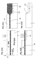
- Figs. 3 and 4 illustrate the process of the manufacturing method of the memory cell shown in Fig. 2.
- a mask 24 for defining the region to form the indentations 4A and 4B is formed after a silicon oxide film 20 and a silicon nitride film 22 are formed on the surface of the p-type silicon semiconductor substrate 1. Then, the silicon nitride film 22 on the region for forming the indentation is etched off utilizing this mask film 24.
- a low concentration n-type region 26 is formed at the surface of the substrate 1 by ion implantation of an n-type dopant such as phosphorus using the patterned silicon nitride film 22 as the mask.
- a thick silicon oxide film 28 is formed in a thermal oxidation atmosphere in the region where an indentation has been formed. Then, as shown in Fig. 3D, the silicon nitride film 22 and the silicon oxide films 20 and 28 are removed. Consequently, the indentation 4 is formed at the surface of the substrate 1 and an n-type region 26 is formed in a region covering from the slope to the bottom of the indentation 4A.
- a three-layer structure ONO consisting of a silicon oxide film, a silicon nitride film and a silicon oxide film is formed on the surface of the substrate and a polysilicon layer 30 is further formed on the three-layer structure ONO.
- the polysilicon layer 30 and the three-layer structure ONO are removed by etching utilizing a mask 32 defining a region for forming the control gate CG.
- the three-layer structure ONO and the control gate CG are formed in the region covering from the horizontal surface of the substrate 1 to the slope of the indentation 4A.
- a p-type region 34 is formed by ion implantation of boron fluoride BF 2 using the control gate CG as the mask.
- This p-type region 34 is the p-type regions 2A and 2B that raise the threshold voltage.
- Fig. 4C side walls 36 and 38 are formed on both sides of the control gate CG and the three-layer structure ONO. Then, the side wall 36 in the region of the indentation 4 (the region of 4A and 4B not shown) is removed by etching using a mask 40. Then, as shown in Fig. 4D, an n-type dopant such as arsenic is ion-implanted using the control gate and the side wall 38 as the masks. As a result, the n-type source region S and the drain region D having high concentrations are formed. Because of the side wall 38, the p-type region 2B on the source region side is remained and the p-type region 34 within the indentation 4A is lost. However, as shown in Fig. 2, in the region except the indentation 4A in the drain region D, the p-type region 2A is remained in the region bordering the channel region.
- the memory cell in the embodiment can be formed in the common semiconductor process.
- Fig. 5 is a plan view of one memory cell.
- the source region S and the drain region D are formed on both of the sides of the control gate CG.
- two mask patterns MA1 and MA2 are used to form the indentations 4A and 4B.
- hot electrons run in the direction denoted by arrows respectively and are injected at the vertical channel regions 10 into the trap gates under the control gate CG.
- the size of the mask patterns MA1 and MA2 are one forth (1/4) of the size of a cell region constituted by the control gate CG and the source and the drain regions S and D, or smaller. However, it is not preferable to use such small-sized masks in terms of process precision.
- Fig. 6 is a plan view of four memory cells.
- four memory cells MC0-MC3 are provided adjacent to each other.
- the memory cells MC0 and MC1 share the drain region D and the memory cells MC2 and MC3 also share the drain region D.
- the memory cells can share the source region S respectively with other four cells (not shown).
- the mask pattern MA1 for forming the indentation can be shared between the memory cell MC0 and MC1 adjacent to each other.
- the mask pattern MA2 can be shared between the memory cell MC0 and MC2 adjacent to each other.
- mask patterns MA3 and MA4 can be also shared between memory cells adjacent to each other.
- the size of these shared mask patterns MA1-MA4 is larger compared to that in the case shown in Fig. 5. Therefore, the problem of low precision in the manufacturing process can be avoided .
- the size of mask patterns MA1-MA4 is approximately same as the size of one memory cell.
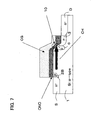
- Fig. 7 is a cross-sectional view illustrating a memory cell improved from the embodiment shown in Fig. 2.
- the memory cell shown in Fig. 7 has a p-type region 6 having a relatively high concentration, provided between the low concentration n-type region 3 formed at the slope (the vertical channel region) in the indentation of the drain region, and the channel region CH.
- the width of the depletion layer in the vertical channel region becomes narrow, the electric field becomes concentrated more, and the hot electrons running in the direction denoted by the arrow are accelerated more and are injected more efficiently to the trap gate on the vertical channel region.
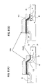
- Fig. 8 shows the extension of the depletion layer of the memory cell shown in Fig. 2 and Fig. 7.
- Fig. 8A shows the extension of the depletion layer 8 of the memory cell shown in Fig. 2. Because the n-type low concentration region 3 is formed in the vertical channel region where the indentation at the drain region side is formed, the depletion layer 8 extends laterally in the vertical channel region 10. Consequently, in the vertical channel region 10, the direction of the electric field generated by the depletion layer 8 is directed from the vertical channel region to the trap gate of three-layer structure ONO.
- Fig. 8B shows the depletion layer 8 for the case where the p-type region 6 is provided in the vertical channel region 10.
- the nonvolatile memory of the embodiment employs a MONOS structure and the periphery of the drain region of the channel region is structured in a vertical channel structure. Therefore, hot electrons running through the horizontal channel region are injected and trapped efficiently to the trap gate formed from a silicon nitride film on the vertical channel region. It is thus possible to lower the voltage needed for programming and to provide a multi-bit nonvolatile memory device whose power voltage is lowered.
- the efficiency of injection of the hot electrons into the trap gate can be made higher by employing a vertical channel structure in the vicinity of the drain region of the channel region.
- a nonvolatile memory device can be provided which allows recording of multi-bit data and lowering of the power voltage.
Landscapes
- Non-Volatile Memory (AREA)
- Semiconductor Memories (AREA)
Abstract
Description
Claims (9)
- A semiconductor nonvolatile memory device for storing multi-bit data, comprising:wherein the memory cell has, at the surface of the semiconductor substrate, an indentation extending from a position in the vicinity of the drain region in the channel region to the drain region, anda memory cell, the memory cell including:a source region and a drain region which are formed at a surface of a semiconductor substrate;a gate insulator film and a control gate which are formed on a channel region between the source region and the drain region; anda nonconductive trap gate in the gate insulator film;
wherein charges are trapped to the trap gate on the indentation. - A semiconductor nonvolatile memory device for storing multi-bit data, comprising:wherein the memory cell has, in a first region which is a part along the gate width, a first indentation extending from a position in the vicinity of the drain region of the channel region to the drain region, anda memory cell, the memory cell including:a source region and a drain region which are formed at a surface of a semiconductor substrate;a gate insulator film and a control gate which are formed on a channel region between the source region and the drain region; anda nonconductive trap gate in the gate insulator film;
wherein the memory cell has, in a second region which is a part along the gate width, different from the first region, a second indentation extending from a position in the vicinity of the source region of the channel region to the source region, and
wherein charges are trapped separately to the trap gate on the first indentation and to the trap gate on the second indentation. - The semiconductor nonvolatile memory device according to claim 2, wherein in the channel region in the vicinity of the drain region, the threshold voltage in a region other than the first region along the gate width is higher than the threshold voltage in the first region for the case where no charges are trapped, and wherein in the channel region in the vicinity of the source region, the threshold voltage in a region other than the second region along the gate width is higher than the threshold voltage in the second region for the case where no charges are trapped.
- The semiconductor nonvolatile memory device according to claim 2, wherein the first indentation and the second indentation are formed at both sides on the diagonal of the channel region.
- The semiconductor nonvolatile memory device according to claim 4, wherein a plurality of memory cell are provided adjacent to each other, the source region and the drain region being shared by the adjacent memory cells, the first and the second indentations being shared by the adjacent memory cells.
- The semiconductor nonvolatile memory device according to claim 1 or 2, further comprising a lightly doped drain region extending from the drain region to the channel region in the indentation, the lightly doped drain region having the same conducting type as the drain region and having a lower concentration than the drain region.
- The semiconductor nonvolatile memory device according to claim 6, further comprising, between the lightly doped drain region and the channel region, a region having the same conducting type as the channel region and having a higher concentration than the channel region.
- A method of manufacturing a semiconductor nonvolatile memory device for storing multi-bit data, the method comprising the steps of:forming indentation at a surface of a semiconductor substrate having a first conducting type;forming a gate insulator film and a control gate on a horizontal surface of the semiconductor substrate and on the surface of the indentation, the gate insulator film embedding a nonconductive trap gate therein;forming a source region of a second conducting type opposite to the first conducting type at the horizontal surface of the semiconductor substrate and a drain region of the second conducting type at the bottom surface of the indentation using the control gate as a mask.
- The method of manufacturing a semiconductor nonvolatile memory device according to claim 8, wherein the indentation is formed in a region which is a part along the gate width, the method further comprising the step of implanting a dopant of the first conducting type into the semiconductor substrate on both sides of the control gate using the control gate as a mask, wherein the step of forming the source region and the drain region includes forming the source region and the drain region by forming side wall layers on the side walls on both sides of the control gate, removing the side wall layer on the indentation, and implanting a dopant of the second conducting type into the semiconductor substrate using the control gate and the remaining side wall layer as a mask.
Applications Claiming Priority (1)
| Application Number | Priority Date | Filing Date | Title |
|---|---|---|---|
| PCT/JP2000/004801 WO2002007215A1 (en) | 2000-07-17 | 2000-07-17 | Nonvolatile memory device and method for manufacturing the same |
Publications (3)
| Publication Number | Publication Date |
|---|---|
| EP1310994A1 true EP1310994A1 (en) | 2003-05-14 |
| EP1310994A4 EP1310994A4 (en) | 2006-01-25 |
| EP1310994B1 EP1310994B1 (en) | 2013-02-13 |
Family
ID=11736271
Family Applications (1)
| Application Number | Title | Priority Date | Filing Date |
|---|---|---|---|
| EP00946371A Expired - Lifetime EP1310994B1 (en) | 2000-07-17 | 2000-07-17 | Nonvolatile memory device and method for manufacturing the same |
Country Status (5)
| Country | Link |
|---|---|
| US (2) | US7057229B2 (en) |
| EP (1) | EP1310994B1 (en) |
| JP (1) | JP4837230B2 (en) |
| KR (1) | KR100706849B1 (en) |
| WO (1) | WO2002007215A1 (en) |
Families Citing this family (6)
| Publication number | Priority date | Publication date | Assignee | Title |
|---|---|---|---|---|
| KR100528466B1 (en) * | 2003-02-12 | 2005-11-15 | 삼성전자주식회사 | Nonvolatile sonos memory device and method for manufacturing the same |
| US7241654B2 (en) * | 2003-12-17 | 2007-07-10 | Micron Technology, Inc. | Vertical NROM NAND flash memory array |
| KR100598106B1 (en) * | 2004-08-27 | 2006-07-07 | 삼성전자주식회사 | Sonos memory cell and its formation method |
| US20060067122A1 (en) * | 2004-09-29 | 2006-03-30 | Martin Verhoeven | Charge-trapping memory cell |
| KR100663008B1 (en) | 2005-07-21 | 2006-12-28 | 동부일렉트로닉스 주식회사 | Drain-extended MOS transistor and manufacturing method thereof |
| KR100644070B1 (en) * | 2005-12-09 | 2006-11-10 | 동부일렉트로닉스 주식회사 | How to manufacture multi-bit flash memory cells |
Family Cites Families (9)
| Publication number | Priority date | Publication date | Assignee | Title |
|---|---|---|---|---|
| JP3159850B2 (en) * | 1993-11-08 | 2001-04-23 | シャープ株式会社 | Nonvolatile semiconductor memory device and method of manufacturing the same |
| JPH08172199A (en) * | 1994-12-20 | 1996-07-02 | Citizen Watch Co Ltd | Semiconductor device and manufacture thereof |
| US5780341A (en) * | 1996-12-06 | 1998-07-14 | Halo Lsi Design & Device Technology, Inc. | Low voltage EEPROM/NVRAM transistors and making method |
| JPH118325A (en) * | 1997-04-25 | 1999-01-12 | Nippon Steel Corp | Nonvolatile semiconductor memory device, manufacturing method thereof, writing method thereof, reading method thereof, recording medium and semiconductor memory device |
| JP3025485B2 (en) * | 1997-12-09 | 2000-03-27 | 松下電器産業株式会社 | Nonvolatile semiconductor memory device and method of manufacturing the same |
| US6121655A (en) * | 1997-12-30 | 2000-09-19 | Matsushita Electric Industrial Co., Ltd. | Nonvolatile semiconductor memory device and method for fabricating the same and semiconductor integrated circuit |
| US6051860A (en) * | 1998-01-16 | 2000-04-18 | Matsushita Electric Industrial Co., Ltd. | Nonvolatile semiconductor memory device and method for fabricating the same and semiconductor integrated circuit |
| US6215148B1 (en) * | 1998-05-20 | 2001-04-10 | Saifun Semiconductors Ltd. | NROM cell with improved programming, erasing and cycling |
| EP1172861A3 (en) * | 2000-07-12 | 2003-11-05 | Matsushita Electric Industrial Co., Ltd. | Nonvolatile semiconductor memory device and method for fabricating the same |
-
2000
- 2000-07-17 EP EP00946371A patent/EP1310994B1/en not_active Expired - Lifetime
- 2000-07-17 KR KR1020037000601A patent/KR100706849B1/en not_active Expired - Fee Related
- 2000-07-17 JP JP2002513018A patent/JP4837230B2/en not_active Expired - Fee Related
- 2000-07-17 WO PCT/JP2000/004801 patent/WO2002007215A1/en not_active Ceased
-
2003
- 2003-01-14 US US10/341,424 patent/US7057229B2/en not_active Expired - Fee Related
-
2006
- 2006-03-23 US US11/386,686 patent/US7462529B2/en not_active Expired - Fee Related
Also Published As
| Publication number | Publication date |
|---|---|
| WO2002007215A1 (en) | 2002-01-24 |
| JP4837230B2 (en) | 2011-12-14 |
| KR100706849B1 (en) | 2007-04-13 |
| US7057229B2 (en) | 2006-06-06 |
| US20060166449A1 (en) | 2006-07-27 |
| EP1310994A4 (en) | 2006-01-25 |
| KR20030019576A (en) | 2003-03-06 |
| US7462529B2 (en) | 2008-12-09 |
| EP1310994B1 (en) | 2013-02-13 |
| US20030104665A1 (en) | 2003-06-05 |
Similar Documents
| Publication | Publication Date | Title |
|---|---|---|
| KR100474176B1 (en) | Method for producing a multi-bit memory cell | |
| US6709922B2 (en) | Method of manufacturing semiconductor integrated circuit device including nonvolatile semiconductor memory devices | |
| US7208794B2 (en) | High-density NROM-FINFET | |
| US20040256661A1 (en) | Nonvolatile memory capable of storing multibits binary information and the method of forming the same | |
| KR100650369B1 (en) | Non-volatile memory device having a polysilicon floating side wall and its manufacturing method | |
| KR20020094913A (en) | Nonvolatile semiconductor memory device and manufacturing method thereof | |
| US20050189582A1 (en) | Charge trapping memory cell and fabrication method | |
| US6190968B1 (en) | Method for forming EPROM and flash memory cells with source-side injection | |
| US6620693B2 (en) | Non-volatile memory and fabrication thereof | |
| JP3821848B2 (en) | 3D non-volatile memory | |
| JP2005142354A (en) | Nonvolatile semiconductor memory device, driving method thereof, and manufacturing method thereof | |
| US6894932B1 (en) | Dual cell memory device having a top dielectric stack | |
| KR100585097B1 (en) | Ypyrom element and its manufacturing method | |
| EP1310994B1 (en) | Nonvolatile memory device and method for manufacturing the same | |
| US20040266109A1 (en) | Semiconductor storage elements, semiconductor device manufacturing methods therefor, portable electronic equipment and IC card | |
| KR100654559B1 (en) | NOR flash memory cell array and manufacturing method thereof | |
| KR101024079B1 (en) | Silicon nitride charge capture memory device | |
| US20080080249A1 (en) | Non-volatile memory, fabricating method and operating method thereof | |
| EP0612108B1 (en) | Double polysilicon EEPROM cell and corresponding manufacturing process | |
| JPWO2002007215A1 (en) | Nonvolatile memory device and method of manufacturing the same | |
| US6868014B1 (en) | Memory device with reduced operating voltage having dielectric stack | |
| KR100545167B1 (en) | Flash memory and manufacturing method thereof | |
| JP5162129B2 (en) | Semiconductor device | |
| US8188536B2 (en) | Memory device and manufacturing method and operating method thereof | |
| US6927128B2 (en) | Method for manufacturing low voltage flash memory |
Legal Events
| Date | Code | Title | Description |
|---|---|---|---|
| PUAI | Public reference made under article 153(3) epc to a published international application that has entered the european phase |
Free format text: ORIGINAL CODE: 0009012 |
|
| 17P | Request for examination filed |
Effective date: 20030115 |
|
| AK | Designated contracting states |
Designated state(s): AT BE CH CY DE DK ES FI FR GB GR IE IT LI LU MC NL PT SE |
|
| RBV | Designated contracting states (corrected) |
Designated state(s): AT BE CH DE FR GB LI |
|
| A4 | Supplementary search report drawn up and despatched |
Effective date: 20051208 |
|
| RAP1 | Party data changed (applicant data changed or rights of an application transferred) |
Owner name: SPANSION, INC. |
|
| GRAP | Despatch of communication of intention to grant a patent |
Free format text: ORIGINAL CODE: EPIDOSNIGR1 |
|
| GRAS | Grant fee paid |
Free format text: ORIGINAL CODE: EPIDOSNIGR3 |
|
| GRAA | (expected) grant |
Free format text: ORIGINAL CODE: 0009210 |
|
| AK | Designated contracting states |
Kind code of ref document: B1 Designated state(s): DE FR GB |
|
| RBV | Designated contracting states (corrected) |
Designated state(s): DE FR GB |
|
| REG | Reference to a national code |
Ref country code: DE Ref legal event code: R081 Ref document number: 60047826 Country of ref document: DE Owner name: CYPRESS SEMICONDUCTOR CORP. (N.D.GES.D.STAATES, US Free format text: FORMER OWNER: FUJITSU LTD., KANAGAWA, JP Ref country code: GB Ref legal event code: FG4D |
|
| REG | Reference to a national code |
Ref country code: DE Ref legal event code: R096 Ref document number: 60047826 Country of ref document: DE Effective date: 20130411 |
|
| PLBE | No opposition filed within time limit |
Free format text: ORIGINAL CODE: 0009261 |
|
| STAA | Information on the status of an ep patent application or granted ep patent |
Free format text: STATUS: NO OPPOSITION FILED WITHIN TIME LIMIT |
|
| 26N | No opposition filed |
Effective date: 20131114 |
|
| REG | Reference to a national code |
Ref country code: DE Ref legal event code: R097 Ref document number: 60047826 Country of ref document: DE Effective date: 20131114 |
|
| PGFP | Annual fee paid to national office [announced via postgrant information from national office to epo] |
Ref country code: DE Payment date: 20140729 Year of fee payment: 15 |
|
| REG | Reference to a national code |
Ref country code: DE Ref legal event code: R082 Ref document number: 60047826 Country of ref document: DE Representative=s name: MURGITROYD & COMPANY, DE Ref country code: DE Ref legal event code: R081 Ref document number: 60047826 Country of ref document: DE Owner name: CYPRESS SEMICONDUCTOR CORP. (N.D.GES.D.STAATES, US Free format text: FORMER OWNER: SPANSION, INC., SUNNYVALE, US |
|
| REG | Reference to a national code |
Ref country code: GB Ref legal event code: 732E Free format text: REGISTERED BETWEEN 20150625 AND 20150701 |
|
| REG | Reference to a national code |
Ref country code: FR Ref legal event code: PLFP Year of fee payment: 16 |
|
| PGFP | Annual fee paid to national office [announced via postgrant information from national office to epo] |
Ref country code: GB Payment date: 20150928 Year of fee payment: 16 |
|
| PGFP | Annual fee paid to national office [announced via postgrant information from national office to epo] |
Ref country code: FR Payment date: 20150917 Year of fee payment: 16 |
|
| REG | Reference to a national code |
Ref country code: DE Ref legal event code: R119 Ref document number: 60047826 Country of ref document: DE |
|
| PG25 | Lapsed in a contracting state [announced via postgrant information from national office to epo] |
Ref country code: DE Free format text: LAPSE BECAUSE OF NON-PAYMENT OF DUE FEES Effective date: 20160202 |
|
| GBPC | Gb: european patent ceased through non-payment of renewal fee |
Effective date: 20160717 |
|
| PG25 | Lapsed in a contracting state [announced via postgrant information from national office to epo] |
Ref country code: FR Free format text: LAPSE BECAUSE OF NON-PAYMENT OF DUE FEES Effective date: 20160801 |
|
| REG | Reference to a national code |
Ref country code: FR Ref legal event code: ST Effective date: 20170331 |
|
| PG25 | Lapsed in a contracting state [announced via postgrant information from national office to epo] |
Ref country code: GB Free format text: LAPSE BECAUSE OF NON-PAYMENT OF DUE FEES Effective date: 20160717 |