Technical Field
This invention relates to a method of manufacturing
dynodes, and relates to a structure of a dynode that is used
for an electron multiplier, a photomultiplier, etc.
Background Art
A dynode, such as one disclosed in Japanese Laid-Open
Patent Application No. S60-182642, in Japanese Laid-Open
Patent Application No. H5-182631, or in Japanese Laid-Open
Patent Application No. H6-314551, is known as this type of
dynode. The dynode disclosed in Japanese Laid-Open Patent
Application No. S60-182642 is a perforated plate member
having a plurality of inwardly curved through-holes (e.g.,
barrel-shaped through-holes), and each of the through-holes
is symmetric about its vertical axis and about a median plane
passing through the dynode. The input and output diameters
of the through-holes are the same, and are smaller than the
diameter of the inside of the through-holes. The dynode
consists of two metal sheets, and is structured such that
the sheets formed by etching are disposed back to back with
each other so as to allow openings larger in diameter of
the convergent or tapered hole to face each other.
The dynode disclosed in Japanese Laid-Open Patent
Application No. H5-182631 and Japanese Laid-Open Patent
Application No. H6-314551 includes a plate having a plurality
of through-holes one end of each of which serves as an input
opening and the other end of each of which serves as an output
opening, and an inner surface of each of the through-holes
has an inclinedpart that inclines with respect to the incident
direction of an electron so that the incident electron from
an incident opening collides therewith. The output opening
of each through-hole is formed to have a bore diameter larger
than the input opening.
Meanwhile, a secondary electron emitted from an
nth-stage dynode ("th" is a suffix used to form ordinal
numbers) is guided by a control electric field formed by
a potential difference between the nth stage and the (n+1)th
stage, and is caused to impinge on the (n+1)th-stage dynode.
In the dynode disclosed in Japanese Laid-Open Patent
Application No. S60-182642, the input diameter and the output
diameter of the through-hole are the same, and therefore
an equipotential line cannot sufficiently enter the inside
of the through-hole of the nth stage that functions as a
control electric field, and, disadvantageously, the control
electric field inside the through-hole is weak. Therefore,
there is a case in which the emitted secondary electron returns
to the side of the nth stage, this forming one cause by which
the efficiency of gathering electrons is lowered.
In contrast, in the dynode disclosed in Japanese
Laid-Open Patent Application No. H5-182631, a through-hole
is formed so that an output opening has a larger bore diameter
than an input opening, and thereby the inner surface of the
through-hole has a tapered shape that becomes gradually wider
toward the output opening. Therefore, a control electric
field for guiding a secondary electron to the next stage
enters the through-hole from the output opening larger in
bore diameter, and rises along the inner surface on the side
opposite to an inclined part, and deeply enters the inside
of the through-hole. As a result, the strength of the control
electric field that can enter the inside of the through-hole
increases, and the emitted secondary electron can be more
reliably guided to the next-stage dynode, thus making it
possible to improve the gathering efficiency of electrons.
Disclosure of the Invention
Generally, as disclosed in Japanese Laid-Open Patent
Application No. S60-182642, Japanese Laid-Open Patent
Application No. H6-314551, etc., a dynode consists of two
sheet metals (two metal plates), and is formed such that
through-holes are formed in each of the sheet metals while
using an etching technique, and, thereafter, the two sheet
metals are bonded together and are integrally united.
However, in the dynode formed by bonding the two sheet
metals together, there is the possibility that misalignment
will occur between the sheet metals when the sheet metals
are bonded together. Therefore, this dynode is at a
disadvantage in the fact that the secondary electron cannot
be appropriately guided because of the misalignment between
the sheet metals, and the gathering efficiency of electrons
decreases. In addition, disadvantageously, there is a need
to design two sheet metals, and, resulting from the fact
that a bonding step must be given in a manufacturing process,
manufacturing costs of the dynode rise.
The present invention has been made in consideration
of the foregoing circumstances. An object of the present
invention is to provide a dynode-manufacturing method and
a dynode structure capable of preventing the gathering
efficiency of electrons from being lowered and capable of
reducing manufacturing costs.
The dynode manufacturing method according to the
present invention is characterized in that the dynode
manufacturing method of forming a through-hole, one end of
which serves as an input opening and the other end of which
serves as an output opening, in a plate has a step of forming
the input opening while etching a predetermined part of one
side surface of the plate in such a way as to draw a first
locus shaped like a substantially circular arc having a
predetermined radius when seen from a direction parallel
to the plate, and a step of forming the output opening while
etching a predetermined part of an opposite surface of the
plate in such a way as to draw a second locus shaped like
a substantially circular arc that is in contact with the
first locus or that overlaps the first locus when seen from
the direction parallel to the plate, in which the second
locus has a predetermined radius when seen from the direction
parallel to the plate, and in which a center of the second
locus is situated with a deviation in the direction parallel
to the plate with respect to a center of the first locus.
In the dynode manufacturing method according to the
present invention, the input opening is formed in one plate
while etching the predetermined part of one side surface
of the plate in such a way as to draw the first locus shaped
like a substantially circular arc having the predetermined
radius when seen from the direction parallel to the plate,
and, on the other hand, the output opening is formed in the
plate while etching the predetermined part of the opposite
surface of the plate in such a way as to draw the second
locus shaped like a substantially circular arc that is in
contact with the first locus or that overlaps the first locus
when seen from the direction parallel to the plate, in which
the second locus has the predetermined radius when seen from
the direction parallel to the plate, and in which the center
of the second locus is situated with a deviation in the
direction parallel to the plate with respect to the center
of the first locus. Therefore, it becomes possible to form
a through-hole in one plate. As a result, it becomes
unnecessary to design two plates and to provide a step of
bonding the plates together, thus making it possible to reduce
the manufacturing costs of dynodes. In addition, since there
is no need to bond two plates together, the misalignment
of the plates bonded together never occurs unlike the
aforementioned case, and an emitted secondary electron can
be appropriately guided to a next-stage dynode, and the
electron-gathering efficiency can be prevented from being
lowered.
Preferably, the radius of the first locus is made smaller
than that of the second locus. If the radius of the first
locus is made smaller than that of the second locus in this
way, a through-hole that has an output opening whose bore
diameter is larger than an input opening can be very easily
formed in a plate. As a result, it is possible to realize
a dynode structured that can further improve
electron-gathering efficiency at low manufacturing costs.
Preferably, the center of the first locus is situated
inside one side surface of the plate when seen from the
direction parallel to the plate. If the center of the first
locus is situated inside one side surface of the plate when
seen from the direction parallel to the plate in this way,
a through-hole that has an output opening whose bore diameter
is larger than an input opening can be very easily formed
in a plate. As a result, it is possible to realize a dynode
structured that can further improve electron-gathering
efficiency at low manufacturing costs.
Preferably, the center of the second locus is situated
inside the opposite surface of the plate or on the opposite
surface of the plate when seen from the direction parallel
to the plate. If the center of the second locus is situated
inside the opposite surface of the plate or on the opposite
surface of the plate when seen from the direction parallel
to the plate in this way, a through-hole that has an output
opening whose bore diameter is larger than an input opening
can be very easily formed in a plate. As a result, it is
possible to realize a dynode structured that can further
improve electron-gathering efficiency at low manufacturing
costs.
The structure of a dynode according to the present
invention is characterized in that the dynode structure has
a through-hole formed in one plate, one end of the through-hole
serving as an input opening, an opposite end thereof serving
as an output opening, in which an inner surface of the
through-hole includes a first curved surface and a second
curved surface that face each other, the first curved surface
extends from an edge of the input opening in such a way as
to face the input opening and is shaped like a substantially
circular arc having a predetermined radius when seen from
a direction parallel to the plate, the second curved surface
extends from an edge of the output opening in such a way
as to face the output opening and is shaped like a substantially
circular arc having a predetermined radius when seen from
the direction parallel to the plate, and the output opening
is formed to have a larger bore diameter than the input opening.
In the dynode structure according to the present
invention, the inner surface of the through-hole includes
the first curved surface and the second curved surface as
described above, and therefore it becomes possible to form
a through-hole in one plate, and it becomes unnecessary to
design two plates and to provide a step of bonding the plates
together, thus making it possible to reduce the manufacturing
costs of dynodes. In addition, since there is no need to
bond two plates together, misalignment of plates bonded
together never occurs unlike the aforementioned case, and,
since the output opening is formed to have a larger bore
diameter than the input opening, an emitted secondary
electron can be appropriately guided to a next-stage dynode,
and the electron-gathering efficiency can be improved.
Preferably, the first curved surface and the second
curved surface are formed such that a locus for forming the
first curved surface and a locus for forming the second curved
surface are in contact with each other or overlap each other.
If the first curved surface and the second curved surface
are formed such that the locus for forming the first curved
surface and the locus for forming the second curved surface
are in contact with each other or overlap each other in this
way, a through-hole can be easily formed, and
dynode-manufacturing costs can be further reduced.
Preferably, the radius of the first curved surface when
seen from the direction parallel to the plate is smaller
than the radius of the second curved surface when seen from
the direction parallel to the plate. If the radius of the
first curved surface when seen from the direction parallel
to the plate is smaller than the radius of the second curved
surface when seen from the direction parallel to the plate,
it is possible to very easily form a through-hole, which
has an output opening whose bore diameter is larger than
an input opening, in the plate. As a result, it is possible
to realize a dynode structured that can further improve
electron-gathering efficiency at low manufacturing costs.
Preferably, the center of the first curved surface is
situated inside one side surface of the plate when seen from
the direction parallel to the plate. If the center of the
first curved surface is situated inside one side surface
of the plate when seen from the direction parallel to the
plate in this way, it is possible to very easily form a
through-hole, which has an output opening whose bore diameter
is larger than an input opening, in the plate. As a result,
it is possible to realize a dynode structured that can further
improve electron-gathering efficiency at low manufacturing
costs.
Preferably, the center of the second curved surface
is situated inside an opposite surface of the plate or on
the opposite surface of the plate when seen from the direction
parallel to the plate. If the center of the second curved
surface is situated inside the opposite surface of the plate
or on the opposite surface of the plate when seen from the
direction parallel to the plate in this way, it is possible
to very easily form a through-hole, which has an output opening
whose bore diameter is larger than an input opening, in the
plate. As a result, it is possible to realize a dynode
structured that can further improve electron-gathering
efficiency at low manufacturing costs.
The dynode structure of the present invention is
characterized in that the dynode structure includes a
metallic plate in which a slit penetrating through upper
and lower surfaces is formed and a
secondary-electron-emitting layer disposed on an inner
surface of the slit, in which each of two inner surfaces
facing each other along a width direction of the slit has
a curved surface that is curved in such a way as to enclose
an axis along a lengthwise direction of the slit, and the
deepest point of one of the curved surfaces along the width
direction is situated outside the slit with respect to a
straight line that extends in a thickness direction of the
metallic plate from an edge of the slit nearest to the deepest
point.
The curved surface does not necessarily need to be a
part of a cylindrical face, and some deformation can be made.
In order to prevent the electron-gathering efficiency from
being lowered, it is necessary that a surface that extends
from the deepest point of at least one of the curved surfaces
to a corresponding edge should overhang. In this case, an
electron can efficiently impinge on an opposite curved
surface.
Brief Description of Drawings
Fig. 1 is a perspective view showing a photomultiplier
according to an embodiment of the present invention.
Fig. 2 is a sectional view along line II-II of Fig.
1.
Fig. 3 is a plan view showing a dynode included in the
photomultiplier according to the embodiment of the present
invention.
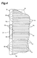
Fig. 4 is an enlarged plan view of a main part of the
dynode included in the photomultiplier according to the
embodiment of the present invention.
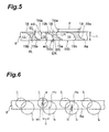
Fig. 5 is a sectional view of the main part of the dynode
included in the photomultiplier according to the embodiment
of the present invention.
Fig. 6 is an explanatory drawing of a manufacturing
method of a dynode included in the photomultiplier according
to the embodiment of the present invention.
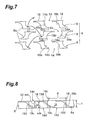
Fig. 7 is a view showing an electron orbit in an electron
multiplier included in the photomultiplier according to the
embodiment of the present invention.
Fig. 8 is a sectional view of a main part showing another
embodiment of the dynode.
Fig. 9 is an explanatory drawing of a manufacturing
method of the dynode shown in Fig. 8.
Fig. 10 is a view showing an electron orbit in an electron
multiplier in which the dynode shown in Fig. 8 is laid on
another dynode so as to form a multilayer.
Best Mode for Carrying Out the Invention
A detailed description will hereinafter be given of
preferred embodiments of a dynode-manufacturing method and
a dynode structure according to the present invention with
reference to the attached drawings. In each figure, the same
reference character is given to the same constituent element,
and a description thereof is omitted. This embodiment shows
an example in which the present invention is applied to a
photomultiplier used for a radiation detector and the like.
Fig. 1 is a perspective view showing a photomultiplier
according to a first embodiment, and Fig. 2 is a sectional
view along line II-II of Fig. 1. The photomultiplier 1 shown
in these figures has a metallic (e.g., Kovar-metallic or
stainless-steel) bypass 2 shaped like a substantially
regularly quadrilateral body. A glass-made (e.g.,
Kovar-glass-made or quartz-glass-made) light-receiving
surface plate 3 is fused and fixed onto an opening end "A"
formed at one side of the bypass 2. A photoelectric plane
3a used to convert light into an electron is formed on the
inner surface of the light-receiving surface plate 3. The
photoelectric plane 3a is formed by causing an alkali metal
to react with antimony that has been vaporously pre-deposited
on the light-receiving surface plate 3. A metallic (e.g.,
Kovar-metallic or stainless-steel) stem plate 4 is welded
and fixed onto an opening end "B" of the bypass 2. A sealed
vessel 5 is made up of the bypass 2, the light-receiving
surface plate 3, and the stem plate 4 in this way. The sealed
vessel 5 is an ultra thin type whose height is about 10 mm.
The light-receiving surface plate 3 may be shaped like a
polygon, such as a rectangle or a hexagon, without being
limited to a square.
A metallic exhaust pipe 6 is fixed to the center of
the stem plate 4. The exhaust pipe 6 is used to expel air
from the inside of the sealed vessel 5 through a vacuum pump
(not shown) so as to create a vacuum therein after completion
of assembly of the photomultiplier 1, and is also used as
a pipe through which an alkali metal vapor is introduced
into the sealed vessel 5 when the photoelectric plane 3a
is molded.
Ablock-like andmultilayered type electron multiplier
7 is disposed in the sealed vessel 5. The electron multiplier
7 has an electron-multiplier part 9 in which ten sheets (ten
stages) of planar dynodes 8 are stacked. In the sealed vessel
5, the electron multiplier 7 is supported by Kovar-metallic
stem pins 10 provided to penetrate through the stem plate
4. The front end of each of the stem pins 10 is electrically
connected to each of the dynodes 8. Pinholes 4a through which
each stem pin 10 penetrates are formed in the stem plate
4. Each pinhole 4a is filled with a tablet 11 that is used
as a Kovar-glass-made hermetic seal. Each stem pin 10 is
fixed to the stem plate 4 by the tablet 11. Concerning the
stem pin 10, there exist a stem pin used for dynodes and
a stem pin used for anodes.
The electron multiplier 7 is provided with anodes 12
that are arranged side by side under the electron-multiplier
part 9 and are each fixed to the upper end of the stem pin
10. On the uppermost stage of the electron multiplier 7,
a flat focusing-electrode plate 13 is disposed between the
photoelectric plane 3a and the electron-multiplier part 9.
A plurality of slit-like openings 13a are formed in the
focusing-electrode plate 13. All of the openings 13a are
arranged to extend in the same direction. Likewise, a
plurality of slit-like electron-multiplier holes 14 used
to multiply electrons are formed and arranged in each dynode
8 of the electron-multiplier part 9. Herein, the
electron-multiplier hole 14 is the through-hole recited in the
appended Claims.
A one-to-one correspondence is made between an
electron-multiplier path L formed by arranging each
electron-multiplier hole 14 of each dynode 8 in the stage
direction and each opening 13a of the focusing-electrode
plate 13, and thereby a plurality of channels are formed
in the electron multiplier 7. The number of anodes 12
disposed in the electron multiplier 7 is 8 x 8 so as to
correspond to each of a predetermined number of channels.
Each anode 12 is connected to each stem pin 10, and thereby
an individual output is drawn out to the outside through
each stem pin 10.
Thus, the electronmultiplier 7 has aplurality of linear
channels. A predetermined voltage is supplied to the
electron-multiplier part 9 and to the anode 12 by the given
stem pin 10 connected to a breeder circuit (not shown) . The
photoelectric plane 3a and the focusing-electrode plate 13
are set at the same potential. The dynodes 8 and the anodes
12 are set to become higher in potential in order from the
uppermost stage. Therefore, light that has impinged on the
light-receiving surface plate 3 is converted into an electron
by the photoelectric plane 3a. This electron enters a
predetermined channel according to an electron-lens effect
formed by the focusing-electrode plate 13 and by the first
dynode 8 placed at the uppermost stage of the electron
multiplier 7. In the channel that the electron has entered,
the electron is subjected to multi-stage multiplication by
the dynodes 8 while following the electron-multiplier path
L of the dynode 8, and impinges on the anode 12. As a result,
an individual output for a predetermined channel is sent
from each anode 12.
Next, referring to Fig. 3 through Fig. 5, the structure
of the aforementioned dynode 8 will be described in detail.
Fig. 3 is a plan view showing the dynode 8, Fig. 4 is an
enlarged plan view of a main part of the dynode 8, and Fig.
5 is a sectional view of the main part of the dynode 8.
Each dynode 8 consists of a plate 8a whose surface has
electric conductivity. Eight-column channels 15 are formed
in each dynode 8. Each channel 15 is made up of enclosures
16 and partition parts 17 of the dynode 8.
Electron-multiplier holes 14 the number of which is the same
as that of the openings 13a of the focusing-electrode plate
13 are arranged in each channel 15 by being subjected to,
for example, chemical etching as described later. All of
the electron-multiplier holes 14 extend in the same direction,
and some of the electron-multiplier holes 14 are arranged
in the direction perpendicular to the sheet. A
multiplier-hole boundary 18 for partitioning is provided
between the electron-multiplier holes 14. The width of the
partition part 17 is determined according to an interval
between the anodes 12, and is greater than that of the
multiplier-hole boundary 18.
A substantially rectangular (about 0.19 mm × about 6.0
mm) input opening 14a, which is one end of the
electron-multiplier hole 14, is formed at the upper surface
of the plate 8a (dynode 8), and a substantially rectangular
(about 0.3 mm × about 6.0 mm) output opening 14b, which is
the other end of the electron-multiplier hole 14, is formed
at the lower surface thereof. The output opening 14b is
formed to have a larger bore diameter than the input opening
14a. In this embodiment, the thickness t of the plate 8a
(dynode 8) is about 0.2 mm, and the pitch p of the
electron-multiplier hole 14 is about 0.5 mm.
An inner surface of the electron-multiplier hole 14
includes a first curved surface 19a and a second curved surface
19b that face each other. The first curved surface 19a
extends from the edge of the input opening 14a in such a
way as to face the input opening 14a, and is shaped like
a substantially circular arc having a predetermined radius
(e.g., about 0.11 mm) when seen from the direction parallel
to the plate 8a. The second curved surface 19b extends from
the edge of the output opening 14b in such a way as to face
the output opening 14b, and is shaped like a substantially
circular arc having a predetermined radius (e.g., about 0.16
mm) when seen from the direction parallel to the plate 8a.
The first curved surface 19a undergoes the vacuum deposition
of antimony (Sb), and, by the reaction of alkali, forms a
secondary-electron-emitting layer.
In this embodiment, the first curved surface 19a and
the second curved surface 19b are formed such that an etching
locus for forming the first curved surface 19a and an etching
locus for forming the second curved surface 19b overlap each
other. The center of the first curved surface 19a is situated
inside one side surface (upper surface) of the plate 8a when
seen from the direction parallel to the plate 8a. The center
of the second curved surface 19b is situated inside the other
surface (lower surface) of the plate 8a when seen from the
direction parallel to the plate 8a. The center of the second
curved surface 19b may be situated on the other surface (lower
surface) of the plate 8a when seen from the direction parallel
to the plate 8a.
A dome-shaped glass part 31 may be bonded and fixed
at predetermined positions of the enclosure 16 and the
partition part 17 of each dynode 8. In this case, the glass
part 31 is provided at a ratio of nine glass parts to one
enclosure 16 or to one partition part 17, and, accordingly,
eighty-one glass parts 31 are provided in total. The glass
part 31 is bonded by applying glass to the enclosure 16 and
to the partition part 17 and hardening it, and is shaped
like a substantially semicircular cylinder whose convex is
directed upward, i.e., a dome-shaped glass part. After the
dome-shaped glass part 31 is bonded, the dynodes 8 are stacked
on each other. As a result, the electron-multiplier part
9 is constructed by the stacked dynodes 8 with the glass
part 31 therebetween.
In this embodiment, the stacked dynodes 8 and the glass
parts 31 are brought into substantially linear contact with
each other, and a joint area between the dynode 8 and the
glass part 31 decreases. Therefore, warping of the dynode
8 can be prevented from occurring, and the dynodes 8 can
be easily stacked on each other. In addition, since the
dome-shaped glass part 31 is provided at predetermined
positions of the enclosure 16 and the partition part 17,
the area of a part (channel 15) where the electron-multiplier
holes 14 are arranged, i.e., the perceptive light receiving
area in the electron multiplier 7 (photomultiplier 1) can
be controlled so as not to be reduced, and, based on this,
the glass part 31 can be bonded to the dynode 8.
Next, the manufacturing method of the dynode 8 will
be described with reference to Fig. 6. The dynode 8 forms
an anti-etching mask having a predetermined shape on the
upper and lower surfaces of the plate 8a, and, after that,
chemical etching is applied to the single plate 8a in the
following way. Thereby, an electron-multiplier hole 14
serving as a through-hole is formed. Chemical etching is
applied to a predetermined part of one side surface (upper
surface) side of the plate 8a in such a way as to draw a
first locus l1 shaped like a substantially circular arc having
a predetermined radius (e.g., about 0.11 mm) when seen from
the direction parallel to the plate 8a, thus forming the
input opening 14a. On the other hand, chemical etching is
applied to a predetermined part of the other surface (lower
surface) side of the plate 8a in such a way as to draw a
second locus l2 shaped like a substantially circular arc,
which has a predetermined radius (e.g., about 0.16 mm) when
seen from the direction parallel to the plate 8a, the center
m2 of which is situated with a deviation in the direction
parallel to the plate 8a with respect to the center m1 of
the first locus l1, and which overlaps the first locus l1
when seen from the direction parallel to the plate 8a, thus
forming the output opening 14b. An interval c in the
direction parallel to the plate 8a between the center m1 of
the first locus l1 and the center m2 of the second locus l2
is set to be about 0.16 mm. When the input opening 14a and
the output opening 14b are formed, a through-hole
(electron-multiplier hole 14) is formed in the plate 8a by
causing the first locus l1 and the second locus l2 to overlap
each other.
In this embodiment, the center m1 of the first locus
l1 is situated inside the upper surface of the plate 8a when
seen from the direction parallel to the plate 8a, and a length
"a" from the upper surface of the plate 8a to the center
m1 of the first locus l1 is set to be about 0.06 mm. On the
other hand, the center m2 of the second locus l2 is situated
inside the lower surface of the plate 8a when seen from the
direction parallel to the plate 8a, and a length "b" from
the lower surface of the plate 8a to the center m2 of the
second locus l2 is set to be about 0.03 mm. The center m2
of the second locus l2 may be situated on the lower surface
of the plate 8a when seen from the direction parallel to
the plate 8a.
Thus, the first curved surface 19a is formedby applying
chemical etching to the plate 8a in such a way as to draw
the first locus l1. The etching depth (ed1/t x 100) of the
first curved surface 19a with respect to the thickness t
of the plate 8a is 85% or more as shown in Fig. 5.
Likewise, the second curved surface 19b is formed by
applying chemical etching to the plate 8a in such a way as
to draw the second locus l2. The etching depth (ed2/t × 100)
of the second curved surface 19b with respect to the thickness
t of the plate 8a is 90% or more as shown in Fig. 5.
Next, referring to Fig. 7, a description will be given
of the operation of the electron multiplier 7
(electron-multiplier part 9) using the dynode 8 structured
as described above.
Fig. 7 shows three consecutive stages of dynodes, which
are taken out from a plurality of stages of the dynodes 8
that constitute the electron-multiplier part 9 of the
electron multiplier 7. The dynodes 8 of the stages are
stacked on each other while reversing the disposing direction
of plates 8a per stage so that the curving direction of the
first curved surface 19a (second curved surface 19b) becomes
opposite between the upper and lower stages.
When a predetermined voltage is applied to each dynode
8 in this state, there are generated an equipotential line
in a state of entering the electron-multiplier hole 14 from
the output opening 14b of the preceding stage while being
curved and an equipotential line in a state of entering the
electron-multiplier hole 14 from the input opening 14a of
the subsequent stage while being curved. Herein, since the
output opening 14b is formed to have a larger bore diameter
than the input opening 14a, the equipotential line entering
from the output opening 14b, i.e., a control electric field
by which a secondary electron is guided to a next stage reaches
a state of deeply entering the interior of the
electron-multiplier hole 14.
The thus deep entering of the equipotential line into
the electron-multiplier hole 14 strengthens the control
electric field of the inside of the electron-multiplier hole
14, and a secondary electron 21 emitted from the lower part
of the first curved surface 19a of the preceding-stage dynode
8 is guided to the subsequent-stage dynode 8.
In the aforementioned embodiment, the first curved
surface 19a and the second curved surface 19b are formed
such that the etching locus for forming the first curved
surface 19a and the etching locus for forming the second
curved surface 19b overlap each other. However, as another
embodiment, the first curved surface 19a and the second curved
surface 19b may be formed such that the etching locus for
forming the first curved surface 19a and the etching locus
for forming the second curved surface 19b come in contact
with each other.
Referring to Fig. 8 through Fig. 10, a description will
hereinafter be given of an embodiment in which the etching
locus for forming the first curved surface 19a and the etching
locus for forming the second curved surface 19b are in contact
with each other.
As shown in Fig. 8, a substantially rectangular (about
0.19 mm x about 6.0 mm) input opening 14c, which is one end
of the electron-multiplier hole 14, is formed in the upper
surface of the plate 8a (dynode 8), and a substantially
rectangular (about 0.3 mm × about 6.0 mm) output opening
14d, which is the other end of the electron-multiplier hole
14, is formed in the lower surface thereof. The output
opening 14d is formed to have a larger bore diameter than
the input opening 14c. In this embodiment, the thickness
t of the plate 8a (dynode 8) is about 0.2 mm, and the pitch
p of the electron-multiplier hole 14 is about 0.5 mm.
An inner surface of the electron-multiplier hole 14
includes a first curved surface 19c and a second curved surface
19d that face each other. The first curved surface 19c
extends from the edge of the input opening 14c in such a
way as to face the input opening 14c, and is shaped like
a substantially circular arc having a predetermined radius
(e.g., about 0.11 mm) when seen from the direction parallel
to the plate 8a. The second curved surface 19d extends from
the edge of the output opening 14d in such a way as to face
the output opening 14d, and is shaped like a substantially
circular arc having a predetermined radius (e.g., about 0.16
mm) when seen from the direction parallel to the plate 8a.
The first curved surface 19c undergoes the vacuum deposition
of antimony (Sb), and, by the reaction of alkali, forms a
secondary-electron-emitting layer.
In this embodiment, the first curved surface 19c and
the second curved surface 19d are formed such that the etching
locus for forming the first curved surface 19c and the etching
locus for forming the second curved surface 19d come in contact
with each other. The center of the first curved surface 19c
is situated inside one side surface (upper surface) of the
plate 8a when seen from the direction parallel to the plate
8a. The center of the second curved surface 19d is situated
inside the other surface (lower surface) of the plate 8a
when seen from the direction parallel to the plate 8a. The
center of the second curved surface 19d may be situated on
the other surface (lower surface) of the plate 8a when seen
from the direction parallel to the plate 8a.
Next, the manufacturing method of the dynode 8 will
be described with reference to Fig. 9. The dynode 8 forms
an anti-etching mask having a predetermined shape on the
upper and lower surfaces of the plate 8a, and, after that,
chemical etching is applied to the single plate 8a in the
following way. Thereby, an electron-multiplier hole 14
serving as a through-hole is formed. Chemical etching is
applied to a predetermined part of one side surface (upper
surface) side of the plate 8a in such a way as to draw a
first locus l3 shaped like a substantially circular arc having
a predetermined radius (e.g., about 0.11 mm) when seen from
the direction parallel to the plate 8a, thus forming the
input opening 14c. On the other hand, chemical etching is
applied to a predetermined part of the other surface (lower
surface) side of the plate 8a in such a way as to draw a
second locus l4 shaped like a substantially circular arc,
which has a predetermined radius (e.g., about 0.16 mm) when
seen from the direction parallel to the plate 8a, the center
m4 of which is situated with a deviation in the direction
parallel to the plate 8a with respect to the center m3 of
the first locus l3, and which overlaps the first locus l3
when seen from the direction parallel to the plate 8a, thus
forming the output opening 14d. An interval h in the
direction parallel to the plate 8a between the center m3 of
the first locus l3 and the center m4 of the second locus l4
is set to be about 0.23 mm. When the input opening 14c and
the output opening 14d are formed, the first locus l3 and
the second locus l4 are caused to come in contact with each
other, and the plate 8a is eroded by the etching, and, as
a result, a through-hole (electron-multiplier hole 14) is
formed in the plate 8a.
In this embodiment, the center m3 of the first locus
l3 is situated inside the upper surface of the plate 8a when
seen from the direction parallel to the plate 8a, and a length
f from the upper surface of the plate 8a to the center m3
of the first locus l3 is set to be about 0.06 mm. On the
other hand, the center m4 of the second locus l4 is situated
inside the lower surface of the plate 8a when seen from the
direction parallel to the plate 8a, and a length g from the
lower surface of the plate 8a to the center m4 of the second
locus l4 is set to be about 0.03 mm. The center m4 of the
second locus l4 may be situated on the lower surface of the
plate 8a when seen from the direction parallel to the plate
8a.
Thus, the first curved surface 19c is formedby applying
chemical etching to the plate 8a in such a way as to draw
the first locus l3. The etching depth (ed3/t × 100) of the
first curved surface 19c with respect to the thickness t
of the plate 8a is 85% or more as shown in Fig. 5.
Likewise, the second curved surface 19d is formed by
applying chemical etching to the plate 8a in such a way as
to draw the second locus l4. The etching depth (ed4/t x 100)
of the second curved surface 19d with respect to the thickness
t of the plate 8a is 90% or more as shown in Fig. 5.
Next, referring to Fig. 10, a description will be given
of the operation of the electron multiplier 7
(electron-multiplier part 9) using the dynode 8 structured
as described above.
Fig. 10 shows three consecutive stages of dynodes, which
are taken out from a plurality of stages of the dynodes 8
that constitute the electron-multiplier part 9 of the
electron multiplier 7. The dynodes 8 of the stages are
stacked on each other while reversing the disposing direction
of plates 8a per stage so that the curving direction of the
first curved surface 19c (second curved surface 19d) becomes
opposite between the upper and lower stages.
When a predetermined voltage is applied to each dynode
8 in this state, there are generated an equipotential line
in a state of entering the electron-multiplier hole 14 from
the output opening 14d of the preceding stage while being
curved and an equipotential line in a state of entering the
electron-multiplier hole 14 from the input opening 14c of
the subsequent stage while being curved. Herein, since the
output opening 14d is formed to have a larger bore diameter
than the input opening 14c, the equipotential line entering
from the output opening 14d, i.e., a control electric field
by which a secondary electron is guided to a next stage reaches
a state of deeply entering the interior of the
electron-multiplier hole 14.
The thus deep entering of the equipotential line into
the electron-multiplier hole 14 strengthens the control
electric field of the inside of the electron-multiplier hole
14, and a secondary electron 21 emitted from the lower part
of the first curved surface 19c of the preceding-stage dynode
8 is guided to the subsequent-stage dynode 8.
Thus, according to the dynode 8 of the aforementioned
embodiments, since the inner surface of the
electron-multiplier hole 14 includes the first curved
surfaces 19a and 19c and the second curved surfaces 19b and
19d as described above, it becomes possible to form the
electron-multiplier hole 14 in the single plate 8a. As a
result, it becomes unnecessary to design two plates and to
provide a step of bonding the plates together, thus making
it possible to reduce the manufacturing costs of the dynode
8. In addition, since there is no need to bond two plates
together, the misalignment of the plates bonded together
never occurs unlike the aforementioned case. Furthermore,
since the output openings 14b and 14d are each formed to
have a larger bore diameter than the input openings 14a and
14c, an emitted secondary electron 21 can be appropriately
guided to the next-stage dynode 8, and electron-gathering
efficiency can be improved.
Furthermore, since the first curved surfaces 19a and
19c and the second curved surfaces 19b and 19d are formed
such that an etching locus (first loci l1, l3) for forming
the first curved surfaces 19a and 19c and an etching locus
(second loci l2, l4) for forming the second curved surfaces
19b and 19d come in contact with each other or overlap each
other, the electron-multiplier hole 14 can be easily formed,
and the manufacturing costs of the dynode 8 can be further
reduced.
Furthermore, since the radius of the first curved
surfaces 19a and 19c is made smaller than that of the second
curved surfaces 19b and 19d when seen from the direction
parallel to the plate 8a, the electron-multiplier hole 14
that has the output openings 14b and 14d whose bore diameter
is larger than the input openings 14a and 14c can be very
easily formed in the plate 8a. As a result, it is possible
to realize the dynode 8 structured that can further improve
electron-gathering efficiency at low manufacturing costs.
Furthermore, since the center of the first curved
surfaces 19a and 19c is situated inside the upper surface
of the plate 8a when seen from the direction parallel to
the plate 8a, the electron-multiplier hole 14 that has the
output openings 14b and 14d whose bore diameter is larger
than the input openings 14a and 14c can be very easily formed
in the plate 8a. As a result, it is possible to realize the
dynode 8 structured that can further improve
electron-gathering efficiency at low manufacturing costs.
Furthermore, since the center of the second curved
surfaces 19b and 19d is situated inside the lower surface
of the plate 8a or on the lower surface thereof when seen
from the direction parallel to the plate 8a, the
electron-multiplier hole 14 that has the output openings
14b and 14d whose bore diameter is larger than the input
openings 14a and 14c can be very easily formed in the plate
8a. As a result, it is possible to realize a dynode 8
structured that can further improve electron-gathering
efficiency at low manufacturing costs.
Further, according to the manufacturing method of the
dynode 8 of the aforementioned embodiments, the input
openings 14a and 14c are formed in the single plate 8a while
etching the predetermined part of the upper surface of the
plate 8a in such a way as to draw the first loci l1, l3 shaped
as mentioned above, and, on the other hand, the output openings
14b and 14d are formed in the plate while applying chemical
etching to the predetermined part of the lower surface of
the plate 8a in such a way as to draw the second loci l2,
l4 shaped as mentioned above. Therefore, it becomes possible
to form the electron-multiplier hole 14a in the single plate
8a. As a result, it becomes unnecessary to design two plates
and to provide a step of bonding the plates together, thus
making it possible to reduce the manufacturing costs of the
dynode. In addition, since there is no need to bond two plates
together, misalignment of the plates bonded together never
occurs unlike the aforementioned case, and an emitted
secondary electron 21 can be appropriately guided to the
next-stage dynode 8, and electron-gathering efficiency can
be prevented from being lowered.
The present invention is not limited to the
aforementioned embodiments, and can be carried out while
appropriately changing the aforementioned numerical values
and shapes. Although an example has been shown in which the
present invention is applied to the photomultiplier 1
including the photoelectric plane 3a, it can, of course,
be applied to an electron multiplier. Additionally, an
etching technique other chemical etching can be used.
The structure of the aforementioned dynode is
characterized in that the dynode structure includes a
metallic plate (dynode 8) in which a slit 14
(electron-multiplier hole) penetrating through its upper
and lower surfaces is formed and secondary-electron-emitting
layers (19a, 19b, 19c, 19d: for convenience of explanation,
they are designated by the same reference characters as the
curved surfaces) disposed on the inner surface of the slit
14, in which each of the two inner surfaces facing each other
along a width direction (direction of the pitch p) of the
slit 14 has a curved surface (19a, 19b, 19c, 19d) that is
curved in such a way as to enclose an axis (m1, m2, m3, m4)
along a lengthwise direction (along the direction
perpendicular to the sheet in Fig. 5 through Fig. 10) of
the slit, and the deepest point (BL, BR) of one of the curved
surfaces along the width direction is situated outside the
slit 14 with respect to a straight line (LL, LR) that extends
in a thickness direction of the metallic plate (dynode 8)
from an edge (EL, ER) of the slit nearest to the deepest
point (BL, BR) (see Fig. 5).
The curved surface does not necessarily need to be a
part of a cylindrical face, and some deformation can be made.
In order to prevent the electron-gathering efficiency from
being lowered, it is necessary that a surface that extends
from the deepest point (BL) of at least one of the curved
surfaces (19a) to a corresponding edge (EL) should overhang.
In this case, an electron can efficiently impinge on the
opposite curved surface 19b. If the curved surface 19b
satisfies the same condition as the curved surface 19a, the
electron-gathering efficiency further increases. These
features are also applied to the dynode shown in Fig. 7 and
in the figures subsequent to this.
As described above in detail, according to the present
invention, it is possible to provide a dynode manufacturing
method and a dynode structure capable of preventing the
electron gathering efficiency from being lowered and capable
of reducing manufacturing costs.
Industrial Applicability
The present invention can be applied to a dynode
manufacturing method and a dynode structure that can be used
for an electron multiplier, a photomultiplier, etc.