EP1310827A2 - Photomask with dust-proofing device and exposure method using the same - Google Patents
Photomask with dust-proofing device and exposure method using the same Download PDFInfo
- Publication number
- EP1310827A2 EP1310827A2 EP02257730A EP02257730A EP1310827A2 EP 1310827 A2 EP1310827 A2 EP 1310827A2 EP 02257730 A EP02257730 A EP 02257730A EP 02257730 A EP02257730 A EP 02257730A EP 1310827 A2 EP1310827 A2 EP 1310827A2
- Authority
- EP
- European Patent Office
- Prior art keywords
- photomask
- transparent substrate
- dust
- transparent
- film
- Prior art date
- Legal status (The legal status is an assumption and is not a legal conclusion. Google has not performed a legal analysis and makes no representation as to the accuracy of the status listed.)
- Granted
Links
Images
Classifications
-
- G—PHYSICS
- G03—PHOTOGRAPHY; CINEMATOGRAPHY; ANALOGOUS TECHNIQUES USING WAVES OTHER THAN OPTICAL WAVES; ELECTROGRAPHY; HOLOGRAPHY
- G03F—PHOTOMECHANICAL PRODUCTION OF TEXTURED OR PATTERNED SURFACES, e.g. FOR PRINTING, FOR PROCESSING OF SEMICONDUCTOR DEVICES; MATERIALS THEREFOR; ORIGINALS THEREFOR; APPARATUS SPECIALLY ADAPTED THEREFOR
- G03F1/00—Originals for photomechanical production of textured or patterned surfaces, e.g., masks, photo-masks, reticles; Mask blanks or pellicles therefor; Containers specially adapted therefor; Preparation thereof
- G03F1/62—Pellicles, e.g. pellicle assemblies, e.g. having membrane on support frame; Preparation thereof
-
- H—ELECTRICITY
- H10—SEMICONDUCTOR DEVICES; ELECTRIC SOLID-STATE DEVICES NOT OTHERWISE PROVIDED FOR
- H10P—GENERIC PROCESSES OR APPARATUS FOR THE MANUFACTURE OR TREATMENT OF DEVICES COVERED BY CLASS H10
- H10P76/00—Manufacture or treatment of masks on semiconductor bodies, e.g. by lithography or photolithography
-
- G—PHYSICS
- G03—PHOTOGRAPHY; CINEMATOGRAPHY; ANALOGOUS TECHNIQUES USING WAVES OTHER THAN OPTICAL WAVES; ELECTROGRAPHY; HOLOGRAPHY
- G03F—PHOTOMECHANICAL PRODUCTION OF TEXTURED OR PATTERNED SURFACES, e.g. FOR PRINTING, FOR PROCESSING OF SEMICONDUCTOR DEVICES; MATERIALS THEREFOR; ORIGINALS THEREFOR; APPARATUS SPECIALLY ADAPTED THEREFOR
- G03F1/00—Originals for photomechanical production of textured or patterned surfaces, e.g., masks, photo-masks, reticles; Mask blanks or pellicles therefor; Containers specially adapted therefor; Preparation thereof
- G03F1/38—Masks having auxiliary features, e.g. special coatings or marks for alignment or testing; Preparation thereof
- G03F1/48—Protective coatings
-
- G—PHYSICS
- G03—PHOTOGRAPHY; CINEMATOGRAPHY; ANALOGOUS TECHNIQUES USING WAVES OTHER THAN OPTICAL WAVES; ELECTROGRAPHY; HOLOGRAPHY
- G03F—PHOTOMECHANICAL PRODUCTION OF TEXTURED OR PATTERNED SURFACES, e.g. FOR PRINTING, FOR PROCESSING OF SEMICONDUCTOR DEVICES; MATERIALS THEREFOR; ORIGINALS THEREFOR; APPARATUS SPECIALLY ADAPTED THEREFOR
- G03F7/00—Photomechanical, e.g. photolithographic, production of textured or patterned surfaces, e.g. printing surfaces; Materials therefor, e.g. comprising photoresists; Apparatus specially adapted therefor
- G03F7/70—Microphotolithographic exposure; Apparatus therefor
- G03F7/708—Construction of apparatus, e.g. environment aspects, hygiene aspects or materials
- G03F7/70983—Optical system protection, e.g. pellicles or removable covers for protection of mask
Definitions
- the present invention relates to a dust-proofing device installed for the purpose of preventing the adhesion of foreign substances to a photomask used in a process of producing high density integrated circuits such as LSIs and VLSIs, and, more particularly, to a photomask equipped with a dust-proofing device which photomask is superior in the transmittance of ultraviolet rays in a short wavelength region and in light resistance and an exposure method using the photomask.
- a pellicle having a structure in which as shown in FIG. 3, an organic thin film formed of nitrocellulose, a fluororesin or the like and having a thickness of several ⁇ m is applied to one side of a frame made of a metal or the like by using an adhesive or the like has been used as a dust-proofing device installed on photomasks used in the production of high density integrated circuits such as LSIs and VLSIs with the intention of preventing the adhesion of foreign substances such as dusts.
- the pellicle is bonded and secured to the photomask after the adhesive is applied to one side of the frame.
- the height of the frame is about 3 to 5 mm in general and the surface of the pellicle film is distant from the pattern surface of the photomask by the height of the frame. Therefore, if fine dusts are stuck to the surface of the pellicle film, the image of these dusts is neither formed on nor transferred to a semiconductor wafer to which a resist is applied during exposure.
- the conventional methods have the problem that since the frame must be secured to the pellicle and the frame must be secured to the photomask by using an adhesive, repeated exposure causes degassing from the adhesive and the decomposition of the adhesive with the result that foreign substances are thereby stuck to the photomask pattern, which causes defects.
- the problems concerning the sticking of foreign substances caused by the adhesive is made more significant as the exposure wavelength is shorter.
- the present invention has been made to solve the aforementioned problems. It is an object of the present invention to provide a photomask equipped with a dust-proofing device which has high ultraviolet transmittance and high resistance to ultraviolet rays and is free from the necessity of the substitution with inert gas and also to provide an exposure method using this photomask.
- a photomask equipped with a dust-proofing device the photomask being produced by overlapping a ultraviolet ray-transmittable transparent substrate on the side of the light-shading film pattern surface of the photomask to apply the photomask to the transparent substrate tightly by exhausting and removing the air present between the light-shading film of the photomask and the transparent substrate.
- the transparent substrate transmitting short wavelength ultraviolet rays a synthetic quartz substrate, single crystal white sapphire, and the like may be used.
- the light-shading film ordinary photomask light-shading materials such as chromium, chromium oxides, chromate nitrides, and the like may be used.
- the removal of the air present between the light-shading film pattern of the photomask and the transparent substrate can be accomplished by placing the photomask and the transparent substrate which are bound tightly with each other in a pure and vacuum chamber which can secure a vacuum of about 133 ⁇ 10 -3 Pa (1 ⁇ 10 -3 Torr) in a clean room and exhausting under vacuum at room temperature for several minutes to tens of minutes .
- degassing of the both may be carried out in advance by evacuation according to the need.
- Technologies for applying the photomask to the thin transparent substrate are exemplified in the publication of Japanese Patent Application Laid-Open No. H6-282066.
- the transparent substrate serves to prevent dusts from adhering directly to the photomask pattern, and also, even if fine dusts adhere to the transparent substrate, the image of these dusts is neither formed on nor transferred to a semiconductor wafer to which a resist is applied during exposure by the aid of the thickness of the transparent substrate. Therefore, the transparent substrate functions as a dust-proofing device. It is only required for the transparent substrate to have a thickness of 2 mm or more which is close to the height of an ordinary pellicle frame because it is only required that the dusts on the transparent substrate are not transferred during exposure. Although it is only required for the transparent substrate to have such a size as to cover the region affecting the transfer of the pattern of the photomask, the transparent substrate preferably has the same size as the photomask from the view point of operation ability.
- a photomask equipped with a dust-proofing device the photomask being produced by forming a transparent film which transmits ultraviolet rays on the entire surface of the side of a light-shading film pattern surface of the photomask and then by overlapping a ultraviolet ray-transmittable transparent substrate on the transparent film to apply the photomask to the transparent substrate tightly by exhausting and removing the air present between the transparent film on the photomask and the transparent substrate.
- the shape and density of the light-shading film pattern of the photomask are diversified and there are photomasks with a light-shading pattern having a small area.
- the transparent film in the present invention is formed to ease the influence of the step caused by the light-shading film pattern to thereby eliminate dependency on a pattern when it is applied to the transparent substrate, thereby more improving the bonding strength between the transparent substrate and the photomask. It is required for the transparent film formed on the photomask to have superior characteristics such as high ultraviolet ray transmittance for exposure wave length and light resistance, and as materials to be used for the transparent film, aluminum oxide, magnesium oxide, magnesium fluoride and the like are shown.
- silicon oxide having a composition close to that of the quartz glass substrate is more preferable as the transparent film.
- a silicon oxide film may be formed by a vacuum deposition method such as sputtering method by Ar gas and by using a SiO 2 target or a coating glass (spin-on-glass; SOG) method.
- SOG spin-on-glass
- OCD Type-2 manufactured by Tokyo Ohka Kogyo Co., Ltd.
- a photomask equipped with a dust-proofing device the photomask being produced by forming a transparent film which transmits ultraviolet rays on the entire surface of the side of a light-shading film pattern surface of the photomask, then by flattening the transparent film, and then by overlapping a ultraviolet ray-transmittable transparent substrate on the transparent film to apply the photomask to the transparent substrate tightly by exhausting and removing the air present between the transparent film flatted on the photomask and the transparent substrate.
- transparent films formed on a photomask have a certain degree of flatness, fine irregularities exist in many transparent films. If fine irregularities of the transparent film which irregularities are produced due to the steps of the light-shading film pattern are removed by polishing and the air present between the transparent film and the transparent substrate is exhausted and removed, the transparent film is bonded with and applied to the entire surface of the transparent substrate.
- the transparent film is polished using a polishing machine by, for example, CMP (Chemical Mechanical Polishing) based on the technologies described in the publication of Japanese Patent Application Laid-Open No. H7-261369 in a predetermined condition.
- CMP Chemical Mechanical Polishing
- an exposure method comprising using the photomask equipped with a dust-proofing device according to the above first aspect to third aspect, removing only the transparent substrate from the photomask to carry out exposure in an exposure apparatus and resetting the transparent substrate to the photomask when the photomask is taken out of the exposure apparatus after the exposure is finished.
- the photomask equipped with a dust-proofing device in the present invention may be used for exposure as it is equipped with the dust-proofing device in the same manner as in the case of using an ordinary pellicle, however, the dust-proofing device can be separated with ease by placing the photomask again under vacuum. To state the influence of dusts adhering to the photomask, these dusts usually adhere most during handling in the atmosphere. In the exposure performed in the ultraviolet region under vacuum, it is needed to improve the transmittance of the photomask for ultraviolet rays as much as possible thereby raising the efficiency of utilization of exposure light.
- One of the objects of the exposure method of the present invention is to raise the efficiency of utilization of exposure light by dismounting the transparent substrate from the photomask equipped with a dust-proofing device in an exposure apparatus to carry out exposure when carrying out exposure to light such as a F 2 laser having a wavelength in the ultraviolet region. After the exposure is finished, the transparent substrate is reset and stuck to the photomask when the photomask is taken out of the exposure apparatus and the ambience around the photomask is then returned to the atmosphere.
- Another object of the exposure method of the present invention resides in the point that an expensive transparent substrate can be reused repeatedly.
- materials which transmit short wavelength ultraviolet rays and the transparent substrate is very expensive.
- such a transparent substrate can be reused many times, if necessary the re-polishing is carried out, and therefore the present invention is also economically advantageous.
- the transparent substrate to be used for the exposure method of the present invention is not necessarily transparent to exposure light because it is dismounted during exposure, however, transparency is needed for the light used for inspection made after the transparent substrate is stuck and applied to the photomask.
- the photomask equipped with a dust-proofing device according to the present invention has high light transmittance even in the case of using aArF (193 nm) excimer laser and F 2 laser (157 nm) whose light sources having short wavelengths ranging from 150 to 200 nm and is highly durable against ultraviolet rays having the same wavelength region, and further, unlike a conventional pellicle, the photomask of the present invention requires no devices for replacing the atmosphere in the inside thereof by inert gas such as nitrogen.
- the dust-proofing device according to the present invention has a structure differing from the structure of a conventional pellicle in which a frame is secured to a photomask by using an adhesive, the dust-proofing device can be separated with ease by again putting the photomask equipped with the dust-proofing device under vacuum. Therefore, when the transparent substrate constituting the dust-proofing device is contaminated with dusts and the like, it is possible to exchange the transparent substrate and to wash both the photomask and the transparent substrate for reuse with ease.
- the exposure method of the present invention has such an effect that the effect of utilization of exposure light is raised to thereby shorten exposure time thereby improving productivity and an expensive transparent substrate can be reused many times.
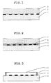
- FIG. 1 is an outlined sectional view of a photomask equipped with a dust-proofing device in Example 1.
- FIG. 2 is an outlined sectional view of a photomask equipped with a dust-proofing device in Example 2.
- FIG. 3 is an outlined view showing a conventional photomask equipped with a pellicle.
- FIG. 1 is a sectional view showing one example of a photomask equipped with a dust-proofing device according to the present invention.
- a photomask in which a light-shading film pattern 2 having a two-layer structure comprising a chromium thin film having 80 nm in thickness and a low reflective chromium thin film having 40 nm in thickness was formed on an optically poll shed synthetic quartz glass substrate 1 which was 6 in. by 6 in. square and had a thickness of 0.25 in. was washed and dried, followed by cleaning its surface.
- a synthetic quartz glass substrate 3 which had the same size as the photomask and a plainness of 2 ⁇ m, was optically polished, washed, and dried, was aligned with the side of the light-shading film pattern surface of the photomask and overlapped on the photomask without using an adhesive or the like.
- the substrate and the photomask were placed in vacuum equipment in an overlapped state, followed by evacuating under a vacuum of 133 ⁇ 10 -3 Pa (1 ⁇ 10 -3 Torr) for 10 minutes to bind both the substrates with each other firmly.
- These two substrates applied in this method were stuck to each other sufficiently and could be used as a photomask equipped with a dust-proofing device in exposure using a ArF excimer laser.
- FIG. 2 shows one example of the present invention.
- a photomask in which a light-shading film pattern 5 having a three-layer structure comprising a center chromium thin film having 60 nm in thickness and low reflective chromium thin films having 40 nm in thickness formed respectively on the upper and lower sides of the above center film was formed on an optically polished synthetic quartz glass substrate which was 6 in. by 6 in. square and had a thickness of 0.25 in. was washed.
- Aquglass 211S which was a commercially available coating glass (spin-on-glass; SOG) manufactured by Allied Signal was applied to the entire surface of the light-shading film pattern by a spin coating method and calcined at 300°C in a nitrogen atmosphere for one hour to obtain a SOG film having a film thickness of about 800 nm as the thickness of the film obtained after calcined.
- SOG was polished by a CMP apparatus SPP600S manufactured by Okamoto Machine Tool Works Ltd. to form a flat SOG film 6 having about 600 nm in thickness.
- the polishing condition was as follows : ILD1300 manufactured by Rodel Nitta Co., was used as the polishing slurry and IC1100 manufactured by Rodel Nitta Co., was used as the polishing cloth, applied load: 50 g/cm 2 , spindle speed: 30 rpm, and table speed: 30 rpm.
- an optically polished synthetic quartz glass substrate 7 which had the same size as the photomask was overlapped on the photomask on the side of the flatted SOG film surface and then placed in vacuum equipment, followed by evacuating at room temperature for 20 minutes to obtain a photomask equipped with a dust-proofing device which was firmly bound with the glass substrate.
- This photomask could be used in exposure using a KrF excimer laser.
- the photomask equipped with a dust-proofing device which was manufactured in Example 1 was placed statically in an exposure apparatus using a F 2 laser. After the atmosphere in the apparatus was evacuated to achieve the vacuum state, the transparent substrate was dismounted from the photomask equipped with a dust-proofing device in the exposure apparatus. Next, the photomask pattern was transferred to a resist on a semiconductor wafer by exposure using a F 2 laser. When the photomask was taken out of the exposure apparatus after the exposure was finished, the pressure in the apparatus was returned to the atmosphere after the transparent substrate was reset to the photomask and the both substrates were bound tightly, and then the photomask was again taken out of the exposure apparatus as a photomask equipped with a dust-proofing device.
Landscapes
- Physics & Mathematics (AREA)
- General Physics & Mathematics (AREA)
- Health & Medical Sciences (AREA)
- Engineering & Computer Science (AREA)
- Environmental & Geological Engineering (AREA)
- Epidemiology (AREA)
- Public Health (AREA)
- Exposure And Positioning Against Photoresist Photosensitive Materials (AREA)
- Preparing Plates And Mask In Photomechanical Process (AREA)
- Exposure Of Semiconductors, Excluding Electron Or Ion Beam Exposure (AREA)
Abstract
Description
Claims (4)
- A photomask equipped with a dust-proofing device, the photomask being produced by overlapping a ultraviolet ray-transmittable transparent substrate on the side of the light-shading film pattern surface of the photomask to apply the photomask to the transparent substrate tightly by exhausting and removing the air present between the light-shading film of the photomask and the transparent substrate.
- A photomask equipped with a dust-proofing device, the photomask being produced by forming a transparent film which transmits ultraviolet rays on the entire surface of the side of a light-shading film pattern surface of the photomask and then by overlapping a ultraviolet ray-transmittable transparent substrate on the transparent film to apply the photomask to the transparent substrate tightly by exhausting and removing the air present between the transparent film on the photomask and the transparent substrate.
- A photomask equipped with a dust-proofing device, the photomask being produced by forming a transparent film which transmits ultraviolet rays on the entire surface of the side of a light-shading film pattern surface of the photomask, then by flattening the transparent film, and then by overlapping a ultraviolet ray-transmittable transparent substrate on the transparent film to apply the photomask to the transparent substrate tightly by exhausting and removing the air present between the transparent film flatted on the photomask and the transparent substrate.
- An exposure method comprising using the photomask equipped with a dust-proofing device according to any one of claims 1 to 3, removing the transparent substrate from the photomask to carry out exposure in an exposure apparatus, resetting the transparent substrate to the photomask after the exposure is finished, and taking out the photomask equipped with a dust-proofing device from the exposure apparatus.
Applications Claiming Priority (2)
| Application Number | Priority Date | Filing Date | Title |
|---|---|---|---|
| JP2001343673 | 2001-11-08 | ||
| JP2001343673A JP3711063B2 (en) | 2001-11-08 | 2001-11-08 | Photomask with dustproof device and exposure method using the same |
Publications (3)
| Publication Number | Publication Date |
|---|---|
| EP1310827A2 true EP1310827A2 (en) | 2003-05-14 |
| EP1310827A3 EP1310827A3 (en) | 2004-07-28 |
| EP1310827B1 EP1310827B1 (en) | 2006-12-20 |
Family
ID=19157320
Family Applications (1)
| Application Number | Title | Priority Date | Filing Date |
|---|---|---|---|
| EP02257730A Expired - Lifetime EP1310827B1 (en) | 2001-11-08 | 2002-11-07 | Photomask with dust-proofing device and exposure method using the same |
Country Status (6)
| Country | Link |
|---|---|
| US (1) | US6933082B2 (en) |
| EP (1) | EP1310827B1 (en) |
| JP (1) | JP3711063B2 (en) |
| KR (1) | KR100875948B1 (en) |
| DE (1) | DE60216882T2 (en) |
| TW (1) | TW552484B (en) |
Families Citing this family (7)
| Publication number | Priority date | Publication date | Assignee | Title |
|---|---|---|---|---|
| US7110195B2 (en) * | 2004-04-28 | 2006-09-19 | International Business Machines Corporation | Monolithic hard pellicle |
| US20060243300A1 (en) * | 2005-04-27 | 2006-11-02 | Patrick Klingbeil | Method for cleaning lithographic apparatus |
| US20070128240A1 (en) * | 2005-12-06 | 2007-06-07 | Peter Krulevitch | Compliant biocompatible packaging scheme based on NiTi shape memory alloys for implantable biomedical microsystems |
| US20070264582A1 (en) * | 2006-05-09 | 2007-11-15 | Taiwan Semiconductor Manufacturing Co., Ltd. | Double-decker mask-pellicle assembly |
| US20080199783A1 (en) * | 2007-02-21 | 2008-08-21 | Taiwan Semiconductor Manufacturing Company, Ltd. | Double-Decker Pellicle-Mask Assembly |
| ES2473216B1 (en) * | 2014-02-20 | 2015-06-02 | Universitat De Barcelona | SURFACE WITH REDUCTION PROPERTIES OF DIFFUSE LIGHT BY WATER CONDENSATION AND PROCEDURE FOR OBTAINING THIS |
| US10983430B2 (en) * | 2018-02-22 | 2021-04-20 | Taiwan Semiconductor Manufacturing Company, Ltd. | Mask assembly and haze acceleration method |
Family Cites Families (12)
| Publication number | Priority date | Publication date | Assignee | Title |
|---|---|---|---|---|
| FR2439418A1 (en) | 1978-10-17 | 1980-05-16 | Censor Patent Versuch | MASK FOR PROJECTING AN IMAGE ON A SEMICONDUCTOR SUBSTRATE |
| JPS55121443A (en) | 1979-03-14 | 1980-09-18 | Mitsubishi Electric Corp | Photomask base plate |
| JPS5629238A (en) | 1979-08-15 | 1981-03-24 | Dainippon Printing Co Ltd | Photomask |
| US4833051A (en) | 1984-08-20 | 1989-05-23 | Nippon Kogaku K.K. | Protective device for photographic masks |
| JP3324005B2 (en) | 1993-03-29 | 2002-09-17 | 大日本印刷株式会社 | Phase shift photomask substrate and method of manufacturing the same |
| KR100311704B1 (en) * | 1993-08-17 | 2001-12-15 | 기타오카 다카시 | Halftone Phase Shift Photomask, Blanks for Halftone Phase Shift Photomask and Manufacturing Method of the Blanks |
| JP3484548B2 (en) | 1994-03-16 | 2004-01-06 | 大日本印刷株式会社 | Blanks for upper shifter type phase shift photomask, upper shifter type phase shift photomask, and methods of manufacturing the same |
| JP3467191B2 (en) * | 1998-08-19 | 2003-11-17 | 信越化学工業株式会社 | Pellicle manufacturing jig and pellicle manufacturing method using the same |
| JP2001083690A (en) | 1999-09-13 | 2001-03-30 | Asahi Glass Co Ltd | Pellicle |
| WO2001035125A1 (en) | 1999-11-05 | 2001-05-17 | Asahi Glass Company, Limited | Antireflection base for ultraviolet and vacuum ultraviolet regions |
| JP2001203145A (en) * | 2000-01-20 | 2001-07-27 | Nikon Corp | Exposure equipment |
| JP2001226872A (en) * | 2000-02-10 | 2001-08-21 | Fukushin Kogyo Kk | Method and system for converting polyester sea-island fiber into microfiber |
-
2001
- 2001-11-08 JP JP2001343673A patent/JP3711063B2/en not_active Expired - Fee Related
-
2002
- 2002-10-25 TW TW091125012A patent/TW552484B/en not_active IP Right Cessation
- 2002-10-29 KR KR1020020066174A patent/KR100875948B1/en not_active Expired - Fee Related
- 2002-11-06 US US10/288,936 patent/US6933082B2/en not_active Expired - Fee Related
- 2002-11-07 DE DE60216882T patent/DE60216882T2/en not_active Expired - Lifetime
- 2002-11-07 EP EP02257730A patent/EP1310827B1/en not_active Expired - Lifetime
Also Published As
| Publication number | Publication date |
|---|---|
| JP3711063B2 (en) | 2005-10-26 |
| US20030087165A1 (en) | 2003-05-08 |
| DE60216882T2 (en) | 2007-10-18 |
| EP1310827B1 (en) | 2006-12-20 |
| TW552484B (en) | 2003-09-11 |
| JP2003149792A (en) | 2003-05-21 |
| EP1310827A3 (en) | 2004-07-28 |
| DE60216882D1 (en) | 2007-02-01 |
| US6933082B2 (en) | 2005-08-23 |
| KR100875948B1 (en) | 2008-12-26 |
| KR20030038382A (en) | 2003-05-16 |
Similar Documents
| Publication | Publication Date | Title |
|---|---|---|
| JP7285682B2 (en) | Planarized extreme ultraviolet lithography blank and fabrication and lithography system therefor | |
| JP6889792B2 (en) | Glass ceramics for ultraviolet lithography and its manufacturing method | |
| KR101169827B1 (en) | Photomasks and Exposure Methods | |
| US6803160B2 (en) | Multi-tone photomask and method for manufacturing the same | |
| US5928817A (en) | Method of protecting an EUV mask from damage and contamination | |
| US20080264441A1 (en) | Method for removing residuals from photomask | |
| CN1695093A (en) | Damascene extreme ultraviolet lithography (euvl) photomask and method of making | |
| EP1421443A2 (en) | Damascene extreme ultraviolet lithography alternative phase shift photomask and method of making | |
| WO2011125407A1 (en) | Photomask unit and method of manufacturing same | |
| JP2008256925A (en) | Pellicle | |
| US6933082B2 (en) | Photomask with dust-proofing device and exposure method using the same | |
| JP3715189B2 (en) | Phase shift mask | |
| US20060134534A1 (en) | Photomask and method for maintaining optical properties of the same | |
| JP4529359B2 (en) | Ultraviolet exposure mask, blank and pattern transfer method | |
| TWM520723U (en) | EUV photomask protective film structure | |
| JPH07261369A (en) | Blanks for upper shifter type phase shift photomask, upper shifter type phase shift photomask and manufacturing methods thereof | |
| JP4202770B2 (en) | Photomask with dustproof device, exposure method, inspection method and correction method | |
| JP3324005B2 (en) | Phase shift photomask substrate and method of manufacturing the same | |
| CN114217503B (en) | Photomask with protection structure and preparation method thereof | |
| KR102067290B1 (en) | Manufacturing method of mask blank, manufacturing method of transfer mask, and manufacturing method of semiconductor device | |
| KR102807049B1 (en) | blank mask and method of fabricating the same | |
| KR20070039910A (en) | Mask blanks and method for manufacturing same and method for manufacturing transfer plate | |
| JP2004241740A (en) | Dustproof device, stencil mask with dustproof device, exposure method, inspection method, and defect correction method | |
| Wasson et al. | Integration of antireflection coatings on EUV absorber stacks | |
| KR200208744Y1 (en) | Reticle without Pellicle |
Legal Events
| Date | Code | Title | Description |
|---|---|---|---|
| PUAI | Public reference made under article 153(3) epc to a published international application that has entered the european phase |
Free format text: ORIGINAL CODE: 0009012 |
|
| AK | Designated contracting states |
Designated state(s): AT BE BG CH CY CZ DE DK EE ES FI FR GB GR IE IT LI LU MC NL PT SE SK TR |
|
| AX | Request for extension of the european patent |
Extension state: AL LT LV MK RO SI |
|
| PUAL | Search report despatched |
Free format text: ORIGINAL CODE: 0009013 |
|
| AK | Designated contracting states |
Kind code of ref document: A3 Designated state(s): AT BE BG CH CY CZ DE DK EE ES FI FR GB GR IE IT LI LU MC NL PT SE SK TR |
|
| AX | Request for extension of the european patent |
Extension state: AL LT LV MK RO SI |
|
| 17P | Request for examination filed |
Effective date: 20041207 |
|
| AKX | Designation fees paid |
Designated state(s): DE FR IT NL |
|
| 17Q | First examination report despatched |
Effective date: 20050701 |
|
| GRAP | Despatch of communication of intention to grant a patent |
Free format text: ORIGINAL CODE: EPIDOSNIGR1 |
|
| GRAS | Grant fee paid |
Free format text: ORIGINAL CODE: EPIDOSNIGR3 |
|
| GRAA | (expected) grant |
Free format text: ORIGINAL CODE: 0009210 |
|
| AK | Designated contracting states |
Kind code of ref document: B1 Designated state(s): DE FR IT NL |
|
| REF | Corresponds to: |
Ref document number: 60216882 Country of ref document: DE Date of ref document: 20070201 Kind code of ref document: P |
|
| ET | Fr: translation filed | ||
| PLBE | No opposition filed within time limit |
Free format text: ORIGINAL CODE: 0009261 |
|
| STAA | Information on the status of an ep patent application or granted ep patent |
Free format text: STATUS: NO OPPOSITION FILED WITHIN TIME LIMIT |
|
| 26N | No opposition filed |
Effective date: 20070921 |
|
| PGFP | Annual fee paid to national office [announced via postgrant information from national office to epo] |
Ref country code: IT Payment date: 20101020 Year of fee payment: 9 |
|
| PGFP | Annual fee paid to national office [announced via postgrant information from national office to epo] |
Ref country code: NL Payment date: 20111111 Year of fee payment: 10 |
|
| REG | Reference to a national code |
Ref country code: NL Ref legal event code: V1 Effective date: 20130601 |
|
| PG25 | Lapsed in a contracting state [announced via postgrant information from national office to epo] |
Ref country code: IT Free format text: LAPSE BECAUSE OF NON-PAYMENT OF DUE FEES Effective date: 20121107 Ref country code: NL Free format text: LAPSE BECAUSE OF NON-PAYMENT OF DUE FEES Effective date: 20130601 |
|
| PGFP | Annual fee paid to national office [announced via postgrant information from national office to epo] |
Ref country code: FR Payment date: 20131120 Year of fee payment: 12 Ref country code: DE Payment date: 20131121 Year of fee payment: 12 |
|
| REG | Reference to a national code |
Ref country code: DE Ref legal event code: R119 Ref document number: 60216882 Country of ref document: DE |
|
| REG | Reference to a national code |
Ref country code: FR Ref legal event code: ST Effective date: 20150731 |
|
| PG25 | Lapsed in a contracting state [announced via postgrant information from national office to epo] |
Ref country code: DE Free format text: LAPSE BECAUSE OF NON-PAYMENT OF DUE FEES Effective date: 20150602 |
|
| PG25 | Lapsed in a contracting state [announced via postgrant information from national office to epo] |
Ref country code: FR Free format text: LAPSE BECAUSE OF NON-PAYMENT OF DUE FEES Effective date: 20141201 |