EP1309176A2 - Systems and methods for sensing marking substrate area coverage using a spectrophotometer - Google Patents
Systems and methods for sensing marking substrate area coverage using a spectrophotometer Download PDFInfo
- Publication number
- EP1309176A2 EP1309176A2 EP02024290A EP02024290A EP1309176A2 EP 1309176 A2 EP1309176 A2 EP 1309176A2 EP 02024290 A EP02024290 A EP 02024290A EP 02024290 A EP02024290 A EP 02024290A EP 1309176 A2 EP1309176 A2 EP 1309176A2
- Authority
- EP
- European Patent Office
- Prior art keywords
- area coverage
- marking
- marking substrate
- reflectance
- substrate area
- Prior art date
- Legal status (The legal status is an assumption and is not a legal conclusion. Google has not performed a legal analysis and makes no representation as to the accuracy of the status listed.)
- Granted
Links
Images


Classifications
-
- H—ELECTRICITY
- H04—ELECTRIC COMMUNICATION TECHNIQUE
- H04N—PICTORIAL COMMUNICATION, e.g. TELEVISION
- H04N1/00—Scanning, transmission or reproduction of documents or the like, e.g. facsimile transmission; Details thereof
- H04N1/46—Colour picture communication systems
- H04N1/56—Processing of colour picture signals
- H04N1/60—Colour correction or control
- H04N1/603—Colour correction or control controlled by characteristics of the picture signal generator or the picture reproducer
- H04N1/6033—Colour correction or control controlled by characteristics of the picture signal generator or the picture reproducer using test pattern analysis
-
- G—PHYSICS
- G03—PHOTOGRAPHY; CINEMATOGRAPHY; ANALOGOUS TECHNIQUES USING WAVES OTHER THAN OPTICAL WAVES; ELECTROGRAPHY; HOLOGRAPHY
- G03G—ELECTROGRAPHY; ELECTROPHOTOGRAPHY; MAGNETOGRAPHY
- G03G2215/00—Apparatus for electrophotographic processes
- G03G2215/00025—Machine control, e.g. regulating different parts of the machine
- G03G2215/00029—Image density detection
- G03G2215/00033—Image density detection on recording member
- G03G2215/00037—Toner image detection
- G03G2215/00042—Optical detection
Definitions
- This invention relates to sensing area coverage of a marking substrate.
- printing systems contain complex control and calibration loops, including internal process control and external color control loops.
- printing systems disclosed in U.S. Patent No. 5,471,313 and U.S. Patent No. 6,236,474 contain levels 1, 2 and 3 control loops aimed at ultimately controlling the toner development process on the photoreceptor belt. These loops measure the state of the image on the photoreceptor by measuring the charge and developed mass per unit area for individual primaries, and actuate the charging and donor roll voltages to maintain the developability to some target set points.
- level 3 loops are designed to produce tone reproduction curves (TRCs) for each color separation (e.g., cyan, magenta, yellow and/or black) by measuring the developed toner mass on the photoreceptor belt.
- TRCs tone reproduction curves
- a sensor such as an ETACS (Enhanced Toner Area Coverage Sensor) sensor system is used in level 2 and 3 loops to measure toner mass on the belt.
- the ETAC sensing head utilizes illumination by a single LED, which is tuned at a specific wavelength and uses a PIN diode as the detector.
- printers use a similar multilevel control architecture with different kinds of sensor.
- the level 2 functionality is achieved using a single LED ADC (Automatic Density Sensor) sensor that measures the toner mass on the belt
- the level 3 functionality is achieved using a Color Patch-On-Paper (C-POP) sensor, which is a sensor that uses a single LED, that measures the toner density of paper-based individual primaries such as C, M, Y and K.
- ADC Automatic Density Sensor
- C-POP Color Patch-On-Paper
- marking substrate area coverage i.e., the mass or density of a marking substance such as toner or ink per unit area of a marking substrate, such as paper or other object to be marked
- marking substrate area coverage i.e., the mass or density of a marking substance such as toner or ink per unit area of a marking substrate, such as paper or other object to be marked
- Calibrating ETAC sensors to toner mass is a long and laborious process, which is almost always done offline and can lead to inaccuracies.
- C-POP sensors are colorblind, and hence cannot differentiate between densities of different color toners.
- a spectrophotometer with multiple illuminants, such as multiple LEDs, for automatic on-line color calibration in a printer or the like.
- a spectrophotometer may be mounted in the paper path of the moving copy sheets in the printer, preferably in the output path after fusing or drying, without having to otherwise modify the printer, or interfere with or interrupt normal printing, or the movement of the printed sheets in said paper path, and yet provide accurate color measurements of test color patches printed on the moving sheets as they pass the spectrophotometer. That enables a complete closed loop color control of a printer.
- marking substrate area coverage refers to the percentage of a given area of a marking substrate that is visibly altered by marking, expressed with respect to the total area. For example, when a yellow patch is created on a marking substrate by depositing dots of yellow toner or ink on the marking substrate, the dots may not completely cover the patch area; therefore, the marking substrate will be only partially covered by the dots. Thus, in this situation, the “marking substrate area coverage” refers to the ratio of the marking substrate within the area of the patch that is covered by the yellow dots to the total area of the patch.
- an on-line sensor is already used in the system for color calibration, this same sensor may also be used as the marking substrate area coverage sensor. Alternatively, a separate sensor may be used as the marking substrate area coverage sensor.
- the marking substrate area coverage sensor obtains reflectance measurements from patches of a marking substrate.
- the marked patches may be patches of a marking substance such as toner, ink or paint, or portions marked by etching or the like.
- a marked patch includes a patch of a marking substance
- the patch is a single-color patch. Coverage information is then extracted from these reflectance measurements.
- the reflectance measurements may be detected after the marking substance has been deposited on a marking substrate, such as a sheet of paper or the like.
- the reflectance measurements may be obtained when the marking substance is in an intermediate state, such as when toner is adhered to a photoreceptor drum or belt prior to being transferred and fused to a marking substrate.
- a Neugebauer model may be used to obtain the reflectance measurements.
- the Neugebauer model uses Neugebauer primaries, which include primary colors such as C, M, Y and K and also include combinations of the primary colors such as CM, CY, CK, MY, MK, etc.
- the weights of Neugebauer primaries represent the fractional area coverage of the primaries.
- This invention rather than using a mixed color model, utilizes the marking substrate area coverage sensor to estimate the fractional area coverage of the individual primaries using their respective reflectance measurements.
- a batch least squares algorithm may be used to estimate the appropriate parameters of the Neugebauer model. For improved accuracy, a recursive least squares algorithm may be used. The recursive least squares algorithm allows the marking substrate area coverage sensor to calibrate itself to changes in the sensing environment.
- the marked patch comprises a marking substance.
- the marking substance is one of ink, toner and paint.
- c is the actual marking substrate area coverage
- ⁇ 1 , ⁇ 2 , ... ⁇ N represent the wavelengths at which reflectance values are measured
- r 1 ( ⁇ ) is the spectral reflectance of the base color of the marking substrate
- r 2 ( ⁇ ) is the spectral reflectance of a marked patch of substantially 100% area coverage
- r( ⁇ ) is a predicted spectral reflectance corresponding to a marked patch under analysis
- n is a Yule-Nielsen correction factor
- N is a number of measured wavelengths of visible light.
- the least squares algorithm minimizes the square of errors between the reference reflectance and the target reflectance.
- This invention provides a marking substrate area coverage sensor with multiple illuminants, such as multiple LEDs.
- the marking substrate area coverage sensor may be the same sensor as a sensor that provides other information, such as color information, used for color calibration.
- a sensor according to this invention can provide information to level 2, 3 and 4 controllers when the level 3 and 4 controllers are implemented by sensing from the paper. Therefore, this invention has the beneficial effect of reducing the number of sensors required.
- Fig. 1 is a functional block diagram illustrating an exemplary embodiment of a marking system 100 according to this invention.
- the marking system 100 is connected to an input device 200 via a link 210.
- the input device 200 inputs various information needed to implement the operations of the marking system 100, as described in more detail below, and may include a mouse, a keyboard, a touch-screen input device, a voice recognition-based input device, and/or any other known or later developed device usable for inputting information.
- the marking system 100 is connected to an image data source 300 via a link 310.
- the image data source 300 can be a digital camera, a scanner, or a locally or remotely located computer, or any other known or later developed device that is capable of generating electronic image data.
- the image data source 300 can be any suitable device that stores and/or transmits electronic image data, such as a client or a server of a network.
- the image data source 300 can be integrated with the marking system 100, as in a digital copier having an integrated scanner.
- the image data source 300 can be connected to the marking system 100 over a connection device, such as a modem, a local area network, a wide area network, an intranet, the Internet, any other distributed processing network, or any other known or later developed connection device.
- the image data source 300 is thus any known or later developed device which is capable of supplying electronic image data over the link 310 to the marking system 100.
- the link 310 can thus be any known or later developed system or device for transmitting the electronic image data from the image data source 300 to the marking system 100.
- the links 210 and 310 can be a wired, wireless or optical link to a network (not shown).
- the network can be a local area network, a wide area network, an intranet, the Internet, or any other distributed processing and storage network.
- the marking system 100 includes a marking device 120, a sensor array 130, a color revision device 140, a memory 150, a controller 160 and a marking substrate area coverage determination system 170, which are interconnected by a data/control bus 190.
- the marking device 120 may be, for example, a print engine/printing head or marking engine/marking head that marks a substrate using any known or later developed marking process, including ink printing processes and xerographic printing processes.
- the sensor array 130 includes multiple illuminants, such as LEDs, lasers or the like, arranged around a central photodetector (not shown), or arranged in correspondence to a plurality of photodetectors or photosites as described in above-mentioned co-pending U.S. Application No. 09/862,247, U.S. Application No. 09/863,042, and/or U.S. Application No. 09/888,791.
- the illuminants will be referred to hereafter as LEDs for convenience.
- the number of LEDs is preferably any number greater than three, when a single photosensor is used, or may be as low as two when multiple photosites or photosensors are used.
- the number of LEDs is preferably from about 8 to about 16.
- the color revision device 140 calibrates the output of the marking device 120 in accordance with information obtained from the sensor array 130. This calibration may be performed as often as necessary or desired to maintain a desirable output of the marking device 120.
- the memory 150 may serve as a buffer for information coming into or going out of the marking system 100, may store any necessary programs and/or data for implementing the functions of the marking system 100, and/or may store data at various stages of processing. Furthermore, it should be appreciated that the memory 150, while depicted as a single entity, may actually be distributed. Alterable portions of the memory 150 are, in various exemplary embodiments, implemented using static or dynamic RAM. However, the memory 150 can also be implemented using a floppy disk and disk drive, a writeable optical disk and disk drive, a hard drive, flash memory or the like. The generally static portions of the memory 150 are, in various exemplary embodiments, implemented using ROM.
- static portions can also be implemented using other non-volatile memory, such as PROM, EPROM, EEPROM, an optical ROM disk, such as a CD-ROM or DVD-ROM, and disk drive, flash memory or other alterable memory, as indicated above, or the like.
- non-volatile memory such as PROM, EPROM, EEPROM, an optical ROM disk, such as a CD-ROM or DVD-ROM, and disk drive, flash memory or other alterable memory, as indicated above, or the like.
- the controller 160 controls the operation of other components of the marking system 100, performs any necessary calculations and executes any necessary programs for implementing the processes of the marking system 100 and its individual components, and controls the flow of data between other components of the marking system 100 as needed. It should be appreciated that the controller may actually include a plurality of discrete circuits, as in the case of the level 1-4 controllers in above-mentioned U.S. Patent No. 5,471,313 and U.S. Patent No. 6,236,474.
- the marking substrate area coverage determination system 170 determines the area coverage of the marking medium in a single-color patch, based on information obtained from the sensor array 130. Exemplary methods for performing this determination using a Neugebauer model are described in detail below. It should be appreciated that, while the same sensor array 130 is used for both color calibration and marking substrate area coverage determination in the embodiment shown in Fig. 1, it is also possible to provide separate sensors for these function. However, in terms of cost, it is advantageous to use one sensor array for both functions.
- each of the circuits shown in Fig. 1 can be implemented as portions of a suitably programmed general purpose computer.
- each of the circuits shown in Fig. 1 can be implemented as physically distinct hardware circuits within an ASIC, or using a FPGA, a PDL, a PLA or a PAL, or using discrete logic elements or discrete circuit elements.
- the particular form each of the circuits shown in Fig. 1 will take is a design choice and will be obvious and predictable to those skilled in the art.
- controller 160 for determining spectra based on the output of the sensor array 130 are described below.
- the reflectance of any halftoned patch is given by the weighted average of the reflectance of its primaries, as described, for example, by M. Xia et al. in "End-To-End Color Printer Calibration by Total Least Squares Regression", IEEE Transactions On Image Processing, Vol. 8 No. 5, May 1999 and/or by R. Balasubramanian in "A Printer Model For Dot-On-Dot Halftone Screens", Proc. SPIE: Color Hard Copy and Graphic Arts IV, vol. 2413, pp. 356-364, 1995, which are both incorporated herein by reference in their entirety.
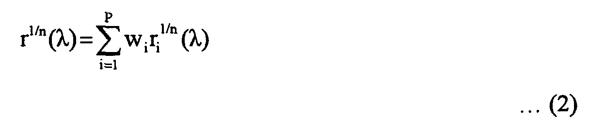
- the basic model shown in equation 1 includes an empirical correction factor n known as the Yule-Nielsen correction factor, and the reflectance of the marked patch under analysis is defined as
- An appropriate value for the Yule-Nielsen correction factor n can be obtained in accordance with a known method for Yule-Nielsen correction, such as that described in the above-mentioned publication by Xia et al.
- the dot area coverage is to be measured for the reproduction of individual separation colors, e.g., cyan or magenta
- the standard Demichel Equations described in the above-mentioned publication by Xia et al. can be used to represent w; in terms of the dot area coverage, c.
- the number of primaries is limited to those reproduced by the single separation color and the base color of the marking substrate, i.e., the color of the original marking substrate before being marked.
- i 2.
- the spectral model can be arranged to contain base color reflectance measurements, r 1 ( ⁇ ).
- r 2 ( ⁇ ) is the reflectance spectra of the primary color with 100% area coverage
- r 1 ( ⁇ ) is the reflectance spectra of the base color of the marking substrate.
- the base color is white.
- the fractional area coverage of the primary color will be measured by the sensor array 130.
- Equation 5 is a linear matrix equation that represents a model of an area coverage sensing system. The problem now becomes how to properly determine area coverage c in a real-world marking system. An exemplary method of estimating c is described below.
- the reflectance of each primary color is measured using a respective marked patch, e.g., color patch, at substantially complete coverage, i.e., about 100% area coverage.
- This reflectance is stored in the sensor database.
- the reflectance of a blank sheet of paper or other substrate is stored in the memory 150 as the base color reflectance. If multiple types of paper or other substrate are to be used, e.g., in multiple supply trays of a photocopier or the like, the reflectance of a blank sheet of each different type of paper or other substrate is measured and stored in the memory 150.
- the corresponding measurements are re-arranged and stored in a matrix A , as shown in equation 6 above, for each type of substrate.
- the Yule-Nielsen correction factor, n is set equal to 1.
- the sensor array 130 measures the reflectance of a marked patch under analysis, e.g., a target patch (preferably a single-color patch) of marking substance under analysis.
- the reflectance data is then re-arranged as shown in vector y above in Equation 6, using the reflectance values for marking substrate base color and r 1 ( ⁇ 1 ), r 1 ( ⁇ 2 ), ... r 1 ( ⁇ N ).
- the area coverage can be obtained by simply solving a least squares problem for a one-time patch measurement.
- Equation 9 can be utilized for extracting area coverage values. However, it is prone to errors due to non-ideal initial conditions, variations from ideal initial conditions, noise in the sensor hardware, variations in temperature, variations in humidity, etc. Hence a recursive adaptive algorithm is preferably used for estimating c. The recursive adaptive algorithm requires making multiple measurements.
- the factor ⁇ is a positive constant, which can be varied to adjust the convergence time (i.e., iteration steps).
- Appropriate values of the factor ⁇ are, for example, in a range from about 1.0 to about 50. Generally, the higher the value of ⁇ , the faster the convergence.
- the number of iterations of the algorithm depends on factors including the desired level of accuracy and the value of the factor ⁇ . Typically, with a factor ⁇ of about 1.5 or above, four, five or six iterations will suffice. A suitable number of iterations may be determined empirically from tests and then preset as the number of iterations to be performed. Alternatively, the process may, for example, determine a percentage change in c and at the end of each iteration, and stop when a desired percentage is reached. For example, the process may automatically stop after the current iteration if c and has not changed more than 1% compared to the previous iteration.
- the sensor array 130 is used for photoreceptor belt or drum area coverage measurements, its measurements are self-calibrating unless the 100% area coverage patch measurement varies with time (that is, when the reflectance spectra of the Neugebauer primary varies with time). If that happens, a one-time sensor calibration should be initiated by printing the Neugebauer primary color at 100% area coverage. This type of sensing does not require the need for a laborious calibration process as is done routinely on ETAC sensors.
- Fig. 2 is a flowchart illustrating an exemplary method of determining marking substrate area coverage according to this invention.
- step S1000 the process continues to step S1100 and obtains a base reflectance of a marking substrate, i.e., the reflectance of an unmarked portion of the substrate.
- step S1200 obtains a reference reflectance, e.g., the reflectance of a marked patch at 100% coverage.
- step S1300 the reflectance of a target marked patch.
- the process then continues to step S1400.
- step S1400 the process obtains an estimated area coverage using the base reflectance, the reference reflectance and the target reflectance.
- the area coverage may be obtained by a least squares equation.
- step S1500 an additional reflectance measurement is obtained from the target patch, and an improved estimate of the area coverage is obtained using an adaptive recursive equation.
- step S1600 the process obtains an estimated area coverage using the base reflectance, the reference reflectance and the target reflectance.
- step S1600 the process determines whether to perform additional iterations of the adaptive recursive equation. This determination may be made in various ways. As one example, a suitable number of iterations may be determined empirically from observation of various tests. For example, if it is known from observation that five iterations generally suffice to give the desired level of accuracy, the process may have five iterations set as a default. Thus, the determination of step S1600 would be based on whether the default number of iterations had been reached.
- the process may compare the new estimate with a previous estimate (e.g., the estimate obtained in step S1400 or in a previous iteration of step S1500), determine the percentage change, and be set to perform additional iterations only when the percentage change is greater than a predetermined amount. For example, when the percentage change from one iteration to the next is only 1% or less, the process may be set to not perform any more iterations.
- a previous estimate e.g., the estimate obtained in step S1400 or in a previous iteration of step S1500
- the process may be set to not perform any more iterations.
- Steps S1500-S1600 are repeated until it is determined in step S1600 to not perform any more iterations of the adaptive recursive equation.
- the process continues to step S1700 and saves the most recent estimate of the area coverage.
- the process then continues to step S1800 and determines whether there are any more marked patches to be measured. If there are any more marked patches to be measured, the process continues to step S1900, selects the next marked patch, and repeats steps S1300-S1800. Otherwise, the process jumps to step S1950 and ends.
- one or more portions of the process shown in Fig. 2 may be omitted.
- this estimate may be sufficiently accurate.
- steps S1500-S1600 may be unnecessary.
- the adaptive recursive equation when used in steps S1500-S1600, the initial estimate of the area coverage, which is used in the first iteration of the adaptive recursive equation, may be obtained by methods other than the method of claim 1400.
- an initial estimate of the area coverage may be input manually, based on the experience or "best guess" of the user, or set as a default.
- step S1400 may be unnecessary in some or all of the cycles of the process of Fig. 2.
- Fig. 3 is a flowchart illustrating an exemplary method of performing color calibration and area coverage calibration according to the invention. Beginning in step S2000, the process continues to step S2100 and obtains both color information and marking substrate area coverage information using a sensor. Next, in step S2200, a color control parameter is revised based on the color information and/or the marking substrate area coverage information obtained in step S2100. The process then continues to step S2300 and ends.
- the marking system 100 of Fig. 1 is preferably implemented either on a single program general purpose computer or separate programmed general purpose computer, with an associated sensor array 130 and marking device 120.
- the marking system 100 can also be implemented on a special purpose computer, a programmed micro-processor or micro-controller and peripheral integrated circuit element, an ASIC or other integrated circuit, a digital signal processor, a hard-wired electronic or logic circuit such as a discrete element circuit, a programmable logic device such as a PLD, PLA, FPGA, PAL, or the like.
- any device capable of implementing a finite state machine that is in turn capable of implementing the flowcharts shown in Fig. 2, or appropriate portions thereof, can be used to implement the marking device according to this invention.
- the disclosed methods may be.readily implemented in software using object or object-oriented software development environments that provide portable source code that can be used on a variety of computer or workstation hardware platforms.
- appropriate portions of the disclosed marking system 100 may be implemented partially or fully in hardware using standard logic circuits or a VLSI design. Whether software or hardware is used to implement the systems in accordance with this invention is dependent on the speed and/or efficiency requirements of the system, the particular function, and the particular software or hardware systems or microprocessor or microcomputer systems being utilized.
- the processing systems and methods described above, however, can be readily implemented in hardware or software using any known or later developed systems or structures, devices and/or software by those skilled in the applicable art without undue experimentation from the functional description provided herein together with a general knowledge of the computer arts.
- the disclosed methods may be readily implemented as software executed on a programmed general purpose computer, a special purpose computer, a micro-processor, or the like.
- the methods and systems of this invention can be implemented as a routine embedded on a personal computer or as a resource residing on a server or workstation, such as a routine embedded in a photocopier, a color photocopier, a printer driver, a scanner, or the like.
- the systems and methods can also be implemented by physical incorporation into a software and/or hardware system, such as the hardware and software system of a photocopier or a dedicated image processing system.
- the invention may apply to any form of marking, e.g., to any process whereby one or more portions of a base object have their appearance altered by another material, such as in painting processes, coil coating or the like, or by a process, such as etching or the like.
- the description above has included various references to color, such as cyan, magenta etc., it should be appreciated that, in embodiments, the invention may apply to single-color marking such as black printing, etching, single-color painting, etc.
Landscapes
- Engineering & Computer Science (AREA)
- Multimedia (AREA)
- Signal Processing (AREA)
- Spectrometry And Color Measurement (AREA)
- Investigating Or Analysing Materials By Optical Means (AREA)
- Facsimile Image Signal Circuits (AREA)
- Control Or Security For Electrophotography (AREA)
Abstract
Description
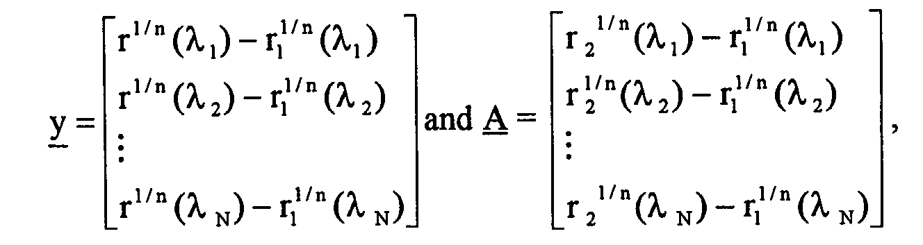
where λ1, λ2, ... λN represent the wavelengths at which reflectance values are measured, r1(λ) is the spectral reflectance of the base color of the marking substrate, r2(λ) is the spectral reflectance of a marked patch of substantially 100% area coverage, r(λ) is a predicted spectral reflectance corresponding to a marked patch under analysis, n is a Yule-Nielsen correction factor, and N is a number of measured wavelengths of visible light.

where λ1, λ2, ... λN represent the wavelengths at which reflectance values are measured, r1(λ) is the spectral reflectance of the base color of the marking substrate, r2(λ) is the spectral reflectance of a marked patch of substantially 100% area coverage, r(λ) is a predicted spectral reflectance corresponding to a marked patch under analysis, n is a Yule-Nielsen correction factor, and N is a number of measured wavelengths of visible light.
In a further embodiment the adaptive equation is defined by



Claims (10)
- A method for sensing marking substrate area coverage using a sensor that comprises a plurality of illuminants and at least one photodetector that receives illumination from the plurality of illuminants, comprising:obtaining marking substrate area coverage information based on information received from the at least one photodetector.
- A marking substrate area coverage sensor, comprising:a plurality of illuminants;at least one photodetector that receives illumination from the plurality of illuminants; anda controller that obtains marking substrate area coverage information based on information from the photodetector.
- A marking system incorporating the marking area coverage sensor of claim 2.
- A method for controlling parameters in a marking system that includes a sensor that outputs both color information and marking substrate area coverage information, comprising:obtaining the color information and the marking substrate area coverage information from the sensor; andrevising at least one color control parameter based on at least one of the color information and the marking substrate area coverage information.
- A marking system parameter control system, comprising:a sensor that outputs both color information and marking substrate area coverage information; andat least one controller that revises at least one color control parameter based on at least one of the color information and the marking substrate area coverage information.
- A marking system incorporating the marking system parameter control system of claim 5.
- A method of obtaining marking substrate area coverage information, comprising:obtaining a base reflectance of an unmarked portion of a marking substrate;obtaining a reference reflectance of a reference marked patch of the marking substrate at substantially complete coverage;obtaining a target reflectance of a target marked patch of the marking substrate; andobtaining an estimated marking substrate area coverage c and of the target marked patch by a least squares algorithm, based on the base reflectance, the reference reflectance and the target reflectance.
- A method of obtaining marking substrate area coverage information, comprising:obtaining a base reflectance of an unmarked portion of a marking substrate;obtaining a reference reflectance of a reference marked patch of the marking substrate at substantially complete coverage;obtaining an initial estimated marking substrate area coverage c and of the target marked patch;obtaining a target reflectance of a target marked patch of the marking substrate;obtaining a first improved estimated marking substrate area coverage c and by an adaptive equation, based on the initial estimated marking substrate area coverage c and, the base reflectance, the reference reflectance and the target reflectance.
- The method of claim 8, further comprising:repeating the obtaining a target reflectance of the target marked patch; andrepeating the obtaining a second improved estimated marking substrate area coverage c and, using the first improved estimated marking substrate area coverage c and as the initial estimated marking substrate area coverage c and, the second improved estimated marking substrate area coverage c and being closer than the first improved estimated marking substrate area coverage c and to actual marking substrate area coverage c.
- A marking system parameter control system, comprising a controller that:obtains a base reflectance of an unmarked portion of a marking substrate;obtains a reference reflectance of a reference marked patch of the marking substrate at substantially complete coverage;obtains an initial estimated marking substrate area coverage c and of the target marked patch;obtains a target reflectance of a target marked patch of the marking substrate;obtains a first improved estimated marking substrate area coverage c and by an adaptive equation, based on the initial estimated marking substrate area coverage c and, the base reflectance, the reference reflectance and the target reflectance.
Applications Claiming Priority (2)
| Application Number | Priority Date | Filing Date | Title |
|---|---|---|---|
| US985419 | 2001-11-02 | ||
| US09/985,419 US7110142B2 (en) | 2001-11-02 | 2001-11-02 | Systems and methods for sensing marking substrate area coverage using a spectrophotometer |
Publications (3)
| Publication Number | Publication Date |
|---|---|
| EP1309176A2 true EP1309176A2 (en) | 2003-05-07 |
| EP1309176A3 EP1309176A3 (en) | 2005-06-15 |
| EP1309176B1 EP1309176B1 (en) | 2008-07-23 |
Family
ID=25531478
Family Applications (1)
| Application Number | Title | Priority Date | Filing Date |
|---|---|---|---|
| EP02024290A Expired - Lifetime EP1309176B1 (en) | 2001-11-02 | 2002-10-31 | Systems and methods for sensing marking substrate area coverage using a spectrophotometer |
Country Status (5)
| Country | Link |
|---|---|
| US (1) | US7110142B2 (en) |
| EP (1) | EP1309176B1 (en) |
| JP (2) | JP2003222588A (en) |
| BR (1) | BR0204548A (en) |
| DE (1) | DE60227761D1 (en) |
Cited By (2)
| Publication number | Priority date | Publication date | Assignee | Title |
|---|---|---|---|---|
| WO2005103836A1 (en) * | 2004-03-25 | 2005-11-03 | Eastman Kodak Company | Densitometer for use in a printer |
| CN102883889A (en) * | 2010-04-07 | 2013-01-16 | 惠普发展公司,有限责任合伙企业 | Color printing system calibration |
Families Citing this family (25)
| Publication number | Priority date | Publication date | Assignee | Title |
|---|---|---|---|---|
| US20040068181A1 (en) * | 2002-09-24 | 2004-04-08 | Konica Corporation | Image forming apparatus, image forming method and image forming system |
| US7059701B2 (en) * | 2004-03-15 | 2006-06-13 | Lexmark International, Inc. | Method for calibrating production printing cartridges for use in an imaging system |
| EP1825419A4 (en) | 2004-11-09 | 2008-08-06 | Digimarc Corp | AUTHENTICATION OF IDENTIFICATION AND SECURITY DOCUMENTS |
| US8154777B2 (en) * | 2005-08-09 | 2012-04-10 | Xerox Corporation | Color compensation of images |
| US7777916B2 (en) * | 2006-04-13 | 2010-08-17 | E. I. Du Pont De Nemours And Company | Method for producing a table of predicted reflectances under target operating conditions and data structure and printing system incorporating the table |
| US7782489B2 (en) * | 2006-04-13 | 2010-08-24 | E.I. Du Pont De Nemours And Company | Method for selecting a sample set useful in relating color reflectances producible under reference and target operating conditions and the sample set producing thereby |
| US8270049B2 (en) * | 2006-08-01 | 2012-09-18 | Xerox Corporation | System and method for high resolution characterization of spatial variance of color separation misregistration |
| US8274717B2 (en) * | 2006-08-01 | 2012-09-25 | Xerox Corporation | System and method for characterizing color separation misregistration |
| US7684082B2 (en) * | 2007-04-19 | 2010-03-23 | Xerox Corporation | Method and system for compensating for thermochromaticity differences in inline spectrophotometers |
| US8228559B2 (en) * | 2007-05-21 | 2012-07-24 | Xerox Corporation | System and method for characterizing color separation misregistration utilizing a broadband multi-channel scanning module |
| US8072648B2 (en) | 2007-07-26 | 2011-12-06 | Xerox Corporation | Halftone independent correction of spatial non-uniformities |
| US8424486B2 (en) | 2008-07-10 | 2013-04-23 | Certusview Technologies, Llc | Marker detection mechanisms for use in marking devices and methods of using same |
| US20100149559A1 (en) * | 2008-12-15 | 2010-06-17 | Xerox Corporation. | Specialty media calibration enhancement method and system |
| CA2691780C (en) | 2009-02-11 | 2015-09-22 | Certusview Technologies, Llc | Management system, and associated methods and apparatus, for providing automatic assesment of a locate operation |
| US8213055B2 (en) * | 2009-02-20 | 2012-07-03 | Hewlett-Packard Development Company, L.P. | Color separation into Neugebauer primary area coverage vectors |
| US8270032B2 (en) * | 2009-10-26 | 2012-09-18 | Hewlett-Packard Development Company, L.P. | Generating color lookup table |
| US8619329B2 (en) | 2010-11-12 | 2013-12-31 | Xerox Corporation | Print smoothness on clear toner enabled systems |
| US8824029B2 (en) * | 2011-06-16 | 2014-09-02 | Cal-Comp Electronics & Communications Company Limited | Color calibration method and image processing device using the same |
| GB2527495A (en) * | 2014-05-20 | 2015-12-30 | Chesapeake Ltd | Ink set optimisation |
| WO2018140055A1 (en) * | 2017-01-30 | 2018-08-02 | Hewlett-Packard Development Company, L.P. | Color calibration |
| WO2018165667A1 (en) | 2017-03-10 | 2018-09-13 | Digimarc Corporation | Predicting detectability and grading prior to printing |
| US10986245B2 (en) | 2017-06-16 | 2021-04-20 | Digimarc Corporation | Encoded signal systems and methods to ensure minimal robustness |
| US10506128B1 (en) | 2017-06-16 | 2019-12-10 | Digimarc Corporation | Encoded signal systems and methods to ensure minimal robustness |
| US10880451B2 (en) | 2018-06-08 | 2020-12-29 | Digimarc Corporation | Aggregating detectability metrics to determine signal robustness |
| CN117214108B (en) * | 2023-11-06 | 2024-02-06 | 安徽猫头鹰科技有限公司 | Batch automatic calibration method based on spectrum detection equipment |
Family Cites Families (16)
| Publication number | Priority date | Publication date | Assignee | Title |
|---|---|---|---|---|
| US5204538A (en) * | 1992-05-18 | 1993-04-20 | Xerox Corporation | Densitometer for an electrophotographic printer using focused and unfocused reflecting beams |
| US5471313A (en) * | 1993-02-24 | 1995-11-28 | Xerox Corporation | Method and control system architecture for controlling tone reproduction in a printing device |
| US5508826A (en) | 1993-04-27 | 1996-04-16 | Lloyd; William J. | Method and apparatus for calibrated digital printing using a four by four transformation matrix |
| US5587728A (en) | 1994-04-29 | 1996-12-24 | International Business Machines Corporation | Optical feedback printer |
| US5519497A (en) * | 1994-11-25 | 1996-05-21 | Xerox Corporation | Control develop mass in a color system |
| US6134029A (en) | 1996-09-09 | 2000-10-17 | Light Source Acquisition Company | Scanner calibration technique |
| US5933578A (en) | 1997-04-08 | 1999-08-03 | Barco Graphics, N.V. | Method and device for determining the color appearance of color overprints |
| US6467867B1 (en) * | 1997-09-03 | 2002-10-22 | Macdermid Acumen, Inc. | Method and apparatus for registration and color fidelity control in a multihead digital color print engine |
| US6236474B1 (en) * | 1998-05-22 | 2001-05-22 | Xerox Corporation | Device independent color controller and method |
| US6650446B1 (en) * | 1999-06-29 | 2003-11-18 | Kodak Polychrome Graphics | Colorimetric characterization of scanned media using spectral scanner and media models |
| US6556932B1 (en) * | 2000-05-01 | 2003-04-29 | Xerox Corporation | System and method for reconstruction of spectral curves using measurements from a color sensor and a spectral measurement system model |
| US6449045B1 (en) * | 2000-05-01 | 2002-09-10 | Xerox Corporation | System and method from reconstruction of spectral curves using measurements for a color sensor and statistical techniques |
| US6628426B2 (en) * | 2001-05-22 | 2003-09-30 | Lexmark International, Inc. | Method of halftone screen linearization via continuous gradient patches |
| US6584435B2 (en) * | 2001-08-30 | 2003-06-24 | Xerox Corporation | Systems and methods for determining spectra using dynamic karhunen-loeve algorithms with measurements from led color sensor |
| US6587793B2 (en) * | 2001-09-17 | 2003-07-01 | Xerox Corporation | Systems and methods for determining spectra using fuzzy inference algorithms with measurements from LED color sensor |
| US7006250B2 (en) * | 2001-09-27 | 2006-02-28 | Lexmark International, Inc. | Method of setting laser power and developer bias in an electrophotographic machine based on an estimated intermediate belt reflectivity |
-
2001
- 2001-11-02 US US09/985,419 patent/US7110142B2/en not_active Expired - Fee Related
-
2002
- 2002-10-30 BR BR0204548-6A patent/BR0204548A/en not_active Application Discontinuation
- 2002-10-30 JP JP2002315279A patent/JP2003222588A/en active Pending
- 2002-10-31 EP EP02024290A patent/EP1309176B1/en not_active Expired - Lifetime
- 2002-10-31 DE DE60227761T patent/DE60227761D1/en not_active Expired - Lifetime
-
2008
- 2008-06-30 JP JP2008170552A patent/JP4799591B2/en not_active Expired - Fee Related
Cited By (4)
| Publication number | Priority date | Publication date | Assignee | Title |
|---|---|---|---|---|
| WO2005103836A1 (en) * | 2004-03-25 | 2005-11-03 | Eastman Kodak Company | Densitometer for use in a printer |
| CN102883889A (en) * | 2010-04-07 | 2013-01-16 | 惠普发展公司,有限责任合伙企业 | Color printing system calibration |
| EP2528738A4 (en) * | 2010-04-07 | 2013-11-20 | Hewlett Packard Development Co | Color printing system calibration |
| CN102883889B (en) * | 2010-04-07 | 2015-04-08 | 惠普发展公司,有限责任合伙企业 | Color printing system calibration |
Also Published As
| Publication number | Publication date |
|---|---|
| JP2008298787A (en) | 2008-12-11 |
| US20030086103A1 (en) | 2003-05-08 |
| EP1309176A3 (en) | 2005-06-15 |
| US7110142B2 (en) | 2006-09-19 |
| JP2003222588A (en) | 2003-08-08 |
| BR0204548A (en) | 2004-06-08 |
| EP1309176B1 (en) | 2008-07-23 |
| DE60227761D1 (en) | 2008-09-04 |
| JP4799591B2 (en) | 2011-10-26 |
Similar Documents
| Publication | Publication Date | Title |
|---|---|---|
| US7110142B2 (en) | Systems and methods for sensing marking substrate area coverage using a spectrophotometer | |
| US7839498B2 (en) | Reference database and method for determining spectra using measurements from an LED color sensor, and method of generating a reference database | |
| US7069164B2 (en) | Method for calibrating a marking system to maintain color output consistency across multiple printers | |
| EP1288640B1 (en) | Systems and methods for determining spectra using dynamic least squares algorithms with measurements from LED color sensor | |
| US6853815B2 (en) | Image forming apparatus and adjustment method of the same | |
| US6584435B2 (en) | Systems and methods for determining spectra using dynamic karhunen-loeve algorithms with measurements from led color sensor | |
| US7295340B2 (en) | Systems and methods for obtaining a spatial color profile, and calibrating a marking system | |
| JP5268542B2 (en) | Image processing apparatus and color processing method | |
| US7271910B2 (en) | Systems and methods for compensating for temperature induced spectral emission variations in LED based color parameter measuring devices | |
| CN107395911B (en) | Image forming apparatus and colour switching control method | |
| US20040131371A1 (en) | Image processing method, image processing apparatus, storage medium, and program | |
| CN101387844A (en) | Color image forming apparatus and color adjustment method | |
| US20130021631A1 (en) | Color printing system calibration | |
| US20050248789A1 (en) | Color image forming apparatus and control method therefor | |
| JP6257148B2 (en) | Image forming apparatus | |
| JP4557944B2 (en) | On-line gray balance calibration with dynamic highlight and shadow control | |
| US7471385B2 (en) | Systems and methods for selecting a reference database for determining a spectrum of an object based on fluorescence of the object | |
| US8514470B2 (en) | Digital printing control using a spectrophotometer | |
| US8351081B2 (en) | Digital printing control using a spectrophotometer | |
| JP2003228201A (en) | Image processing control method and image forming apparatus | |
| JP2001086297A (en) | Luminous quantity measurement device and color image forming apparatus | |
| JP6450444B2 (en) | Measuring apparatus and image forming apparatus | |
| JP2003195583A (en) | Image forming device | |
| JP2005027276A (en) | Image forming method and apparatus |
Legal Events
| Date | Code | Title | Description |
|---|---|---|---|
| PUAI | Public reference made under article 153(3) epc to a published international application that has entered the european phase |
Free format text: ORIGINAL CODE: 0009012 |
|
| AK | Designated contracting states |
Designated state(s): AT BE BG CH CY CZ DE DK EE ES FI FR GB GR IE IT LI LU MC NL PT SE SK TR |
|
| AX | Request for extension of the european patent |
Extension state: AL LT LV MK RO SI |
|
| PUAL | Search report despatched |
Free format text: ORIGINAL CODE: 0009013 |
|
| AK | Designated contracting states |
Kind code of ref document: A3 Designated state(s): AT BE BG CH CY CZ DE DK EE ES FI FR GB GR IE IT LI LU MC NL PT SE SK TR |
|
| AX | Request for extension of the european patent |
Extension state: AL LT LV MK RO SI |
|
| 17P | Request for examination filed |
Effective date: 20051215 |
|
| AKX | Designation fees paid |
Designated state(s): DE FR GB |
|
| 17Q | First examination report despatched |
Effective date: 20061122 |
|
| GRAP | Despatch of communication of intention to grant a patent |
Free format text: ORIGINAL CODE: EPIDOSNIGR1 |
|
| GRAS | Grant fee paid |
Free format text: ORIGINAL CODE: EPIDOSNIGR3 |
|
| GRAA | (expected) grant |
Free format text: ORIGINAL CODE: 0009210 |
|
| AK | Designated contracting states |
Kind code of ref document: B1 Designated state(s): DE FR GB |
|
| REG | Reference to a national code |
Ref country code: GB Ref legal event code: FG4D |
|
| REF | Corresponds to: |
Ref document number: 60227761 Country of ref document: DE Date of ref document: 20080904 Kind code of ref document: P |
|
| PLBE | No opposition filed within time limit |
Free format text: ORIGINAL CODE: 0009261 |
|
| STAA | Information on the status of an ep patent application or granted ep patent |
Free format text: STATUS: NO OPPOSITION FILED WITHIN TIME LIMIT |
|
| 26N | No opposition filed |
Effective date: 20090424 |
|
| REG | Reference to a national code |
Ref country code: FR Ref legal event code: PLFP Year of fee payment: 15 |
|
| PGFP | Annual fee paid to national office [announced via postgrant information from national office to epo] |
Ref country code: GB Payment date: 20160928 Year of fee payment: 15 |
|
| PGFP | Annual fee paid to national office [announced via postgrant information from national office to epo] |
Ref country code: FR Payment date: 20160921 Year of fee payment: 15 |
|
| PGFP | Annual fee paid to national office [announced via postgrant information from national office to epo] |
Ref country code: DE Payment date: 20160922 Year of fee payment: 15 |
|
| REG | Reference to a national code |
Ref country code: DE Ref legal event code: R119 Ref document number: 60227761 Country of ref document: DE |
|
| GBPC | Gb: european patent ceased through non-payment of renewal fee |
Effective date: 20171031 |
|
| REG | Reference to a national code |
Ref country code: FR Ref legal event code: ST Effective date: 20180629 |
|
| PG25 | Lapsed in a contracting state [announced via postgrant information from national office to epo] |
Ref country code: GB Free format text: LAPSE BECAUSE OF NON-PAYMENT OF DUE FEES Effective date: 20171031 Ref country code: DE Free format text: LAPSE BECAUSE OF NON-PAYMENT OF DUE FEES Effective date: 20180501 |
|
| PG25 | Lapsed in a contracting state [announced via postgrant information from national office to epo] |
Ref country code: FR Free format text: LAPSE BECAUSE OF NON-PAYMENT OF DUE FEES Effective date: 20171031 |