EP1309173A2 - Image data processing device processing plurality of series of data items simultaneously in parallel - Google Patents
Image data processing device processing plurality of series of data items simultaneously in parallel Download PDFInfo
- Publication number
- EP1309173A2 EP1309173A2 EP02257566A EP02257566A EP1309173A2 EP 1309173 A2 EP1309173 A2 EP 1309173A2 EP 02257566 A EP02257566 A EP 02257566A EP 02257566 A EP02257566 A EP 02257566A EP 1309173 A2 EP1309173 A2 EP 1309173A2
- Authority
- EP
- European Patent Office
- Prior art keywords
- image
- data
- image data
- series
- memory
- Prior art date
- Legal status (The legal status is an assumption and is not a legal conclusion. Google has not performed a legal analysis and makes no representation as to the accuracy of the status listed.)
- Granted
Links
- 238000012545 processing Methods 0.000 title claims description 191
- 230000015654 memory Effects 0.000 claims abstract description 389
- 238000006243 chemical reaction Methods 0.000 claims abstract description 315
- 238000000034 method Methods 0.000 claims abstract description 271
- 230000008569 process Effects 0.000 claims abstract description 262
- 239000000872 buffer Substances 0.000 claims abstract description 108
- 239000011159 matrix material Substances 0.000 claims description 92
- 238000012546 transfer Methods 0.000 claims description 76
- 238000004364 calculation method Methods 0.000 claims description 64
- 238000012937 correction Methods 0.000 claims description 64
- 238000003860 storage Methods 0.000 claims description 38
- 230000006870 function Effects 0.000 claims description 23
- 238000007639 printing Methods 0.000 claims description 19
- 230000014509 gene expression Effects 0.000 claims description 16
- 238000013500 data storage Methods 0.000 claims description 8
- 230000002093 peripheral effect Effects 0.000 claims description 6
- 230000000717 retained effect Effects 0.000 claims description 5
- 238000003672 processing method Methods 0.000 claims description 4
- 230000002194 synthesizing effect Effects 0.000 claims description 4
- 238000004590 computer program Methods 0.000 claims 1
- 238000001514 detection method Methods 0.000 description 71
- 238000000926 separation method Methods 0.000 description 53
- 101100278839 Drosophila melanogaster sw gene Proteins 0.000 description 48
- 238000010586 diagram Methods 0.000 description 22
- 102100021935 C-C motif chemokine 26 Human genes 0.000 description 16
- 101000897493 Homo sapiens C-C motif chemokine 26 Proteins 0.000 description 16
- 239000003086 colorant Substances 0.000 description 16
- 230000006835 compression Effects 0.000 description 15
- 238000007906 compression Methods 0.000 description 15
- 238000009826 distribution Methods 0.000 description 12
- 238000001914 filtration Methods 0.000 description 12
- 230000004044 response Effects 0.000 description 12
- 238000003705 background correction Methods 0.000 description 9
- 238000004042 decolorization Methods 0.000 description 9
- 238000003379 elimination reaction Methods 0.000 description 8
- 230000001965 increasing effect Effects 0.000 description 8
- 101000860173 Myxococcus xanthus C-factor Proteins 0.000 description 6
- 238000004891 communication Methods 0.000 description 6
- 230000015572 biosynthetic process Effects 0.000 description 5
- 230000008030 elimination Effects 0.000 description 5
- 230000005540 biological transmission Effects 0.000 description 4
- 230000000903 blocking effect Effects 0.000 description 4
- 230000007423 decrease Effects 0.000 description 4
- 230000003247 decreasing effect Effects 0.000 description 4
- 238000009499 grossing Methods 0.000 description 4
- 230000003287 optical effect Effects 0.000 description 4
- 230000007704 transition Effects 0.000 description 4
- 230000008859 change Effects 0.000 description 3
- 230000006866 deterioration Effects 0.000 description 3
- 230000000873 masking effect Effects 0.000 description 3
- 241000519995 Stachys sylvatica Species 0.000 description 2
- 238000004458 analytical method Methods 0.000 description 2
- 238000003708 edge detection Methods 0.000 description 2
- 238000005516 engineering process Methods 0.000 description 2
- 238000000605 extraction Methods 0.000 description 2
- 239000000314 lubricant Substances 0.000 description 2
- 239000000463 material Substances 0.000 description 2
- 230000007246 mechanism Effects 0.000 description 2
- 230000010355 oscillation Effects 0.000 description 2
- 239000000843 powder Substances 0.000 description 2
- 230000009467 reduction Effects 0.000 description 2
- 230000004304 visual acuity Effects 0.000 description 2
- 229920002799 BoPET Polymers 0.000 description 1
- 235000006679 Mentha X verticillata Nutrition 0.000 description 1
- 235000002899 Mentha suaveolens Nutrition 0.000 description 1
- 235000001636 Mentha x rotundifolia Nutrition 0.000 description 1
- 239000005041 Mylar™ Substances 0.000 description 1
- 239000002033 PVDF binder Substances 0.000 description 1
- 238000013019 agitation Methods 0.000 description 1
- 238000004140 cleaning Methods 0.000 description 1
- 239000004020 conductor Substances 0.000 description 1
- 125000004122 cyclic group Chemical group 0.000 description 1
- 230000005684 electric field Effects 0.000 description 1
- 230000002708 enhancing effect Effects 0.000 description 1
- 238000005286 illumination Methods 0.000 description 1
- 238000003780 insertion Methods 0.000 description 1
- 230000037431 insertion Effects 0.000 description 1
- 239000010410 layer Substances 0.000 description 1
- 238000012986 modification Methods 0.000 description 1
- 230000004048 modification Effects 0.000 description 1
- 230000000644 propagated effect Effects 0.000 description 1
- 238000013139 quantization Methods 0.000 description 1
- 230000002829 reductive effect Effects 0.000 description 1
- 230000002441 reversible effect Effects 0.000 description 1
- 230000000630 rising effect Effects 0.000 description 1
- 102220032891 rs367543178 Human genes 0.000 description 1
- 239000002356 single layer Substances 0.000 description 1
- 239000000126 substance Substances 0.000 description 1
- 238000003786 synthesis reaction Methods 0.000 description 1
- 238000005494 tarnishing Methods 0.000 description 1
- 230000001960 triggered effect Effects 0.000 description 1
- 238000011144 upstream manufacturing Methods 0.000 description 1
- 239000002699 waste material Substances 0.000 description 1
- 238000005303 weighing Methods 0.000 description 1
Images

















Classifications
-
- H—ELECTRICITY
- H04—ELECTRIC COMMUNICATION TECHNIQUE
- H04N—PICTORIAL COMMUNICATION, e.g. TELEVISION
- H04N1/00—Scanning, transmission or reproduction of documents or the like, e.g. facsimile transmission; Details thereof
- H04N1/32—Circuits or arrangements for control or supervision between transmitter and receiver or between image input and image output device, e.g. between a still-image camera and its memory or between a still-image camera and a printer device
- H04N1/32561—Circuits or arrangements for control or supervision between transmitter and receiver or between image input and image output device, e.g. between a still-image camera and its memory or between a still-image camera and a printer device using a programmed control device, e.g. a microprocessor
-
- H—ELECTRICITY
- H04—ELECTRIC COMMUNICATION TECHNIQUE
- H04N—PICTORIAL COMMUNICATION, e.g. TELEVISION
- H04N1/00—Scanning, transmission or reproduction of documents or the like, e.g. facsimile transmission; Details thereof
- H04N1/32—Circuits or arrangements for control or supervision between transmitter and receiver or between image input and image output device, e.g. between a still-image camera and its memory or between a still-image camera and a printer device
- H04N1/32561—Circuits or arrangements for control or supervision between transmitter and receiver or between image input and image output device, e.g. between a still-image camera and its memory or between a still-image camera and a printer device using a programmed control device, e.g. a microprocessor
- H04N1/32571—Details of system components
- H04N1/32587—Controller
-
- H—ELECTRICITY
- H04—ELECTRIC COMMUNICATION TECHNIQUE
- H04N—PICTORIAL COMMUNICATION, e.g. TELEVISION
- H04N1/00—Scanning, transmission or reproduction of documents or the like, e.g. facsimile transmission; Details thereof
- H04N1/32—Circuits or arrangements for control or supervision between transmitter and receiver or between image input and image output device, e.g. between a still-image camera and its memory or between a still-image camera and a printer device
- H04N1/32561—Circuits or arrangements for control or supervision between transmitter and receiver or between image input and image output device, e.g. between a still-image camera and its memory or between a still-image camera and a printer device using a programmed control device, e.g. a microprocessor
- H04N1/32593—Using a plurality of controllers, e.g. for controlling different interfaces
-
- H—ELECTRICITY
- H04—ELECTRIC COMMUNICATION TECHNIQUE
- H04N—PICTORIAL COMMUNICATION, e.g. TELEVISION
- H04N1/00—Scanning, transmission or reproduction of documents or the like, e.g. facsimile transmission; Details thereof
- H04N1/32—Circuits or arrangements for control or supervision between transmitter and receiver or between image input and image output device, e.g. between a still-image camera and its memory or between a still-image camera and a printer device
- H04N1/32561—Circuits or arrangements for control or supervision between transmitter and receiver or between image input and image output device, e.g. between a still-image camera and its memory or between a still-image camera and a printer device using a programmed control device, e.g. a microprocessor
- H04N1/32598—Bus based systems
- H04N1/32603—Multi-bus systems
-
- H—ELECTRICITY
- H04—ELECTRIC COMMUNICATION TECHNIQUE
- H04N—PICTORIAL COMMUNICATION, e.g. TELEVISION
- H04N1/00—Scanning, transmission or reproduction of documents or the like, e.g. facsimile transmission; Details thereof
- H04N1/40—Picture signal circuits
- H04N1/407—Control or modification of tonal gradation or of extreme levels, e.g. background level
-
- H—ELECTRICITY
- H04—ELECTRIC COMMUNICATION TECHNIQUE
- H04N—PICTORIAL COMMUNICATION, e.g. TELEVISION
- H04N2201/00—Indexing scheme relating to scanning, transmission or reproduction of documents or the like, and to details thereof
- H04N2201/0077—Types of the still picture apparatus
- H04N2201/0094—Multifunctional device, i.e. a device capable of all of reading, reproducing, copying, facsimile transception, file transception
Definitions
- the present invention generally relates to a data conversion device, an image data processing device, a data conversion method, a pattern matching method, and an image data processing method, and more particularly, to an image processing device using the data conversion device, and an image processing device using the image data processing device.
- a data processing amount by a computer has been increased, more often involving data conversions or corrections.
- image data processes such as: reading corrections (a CCD inter-line correction, a main-scanning resist adjustment, a shading correction, a dot correction, a vertical stripe correction, a ⁇ conversion, etc.) for compensating or correcting reading distortions of RGB image data read by a document scanner; an image area separation of judging whether a read image is an edge (a character edge) or an inside (within a line width: a character inside) of a part having a binary shade (hereinafter simply referred to as character ), such as a character or a line, whether a halftone (dot) image, such as a photograph (hereinafter simply referred to as photograph), or further whether chromatic or achromatic; intermediate processes (a filtering process, a ground-color removal, a color conversion,
- a buffer memory device is used in an image data process.
- Japanese Laid-Open Patent Application No. 8-305329 discloses a signal processing device in which: an input data selector 6, an input data latch 10, one memory unit 1, an output data latch 11, and an output data selector 9 are connected in this order along the course of data; further, a writing address selector 7, a reading address selector 8, and a CPU 12 controlling each of the selectors are provided; in this structure, the memory unit 1 is used selectively as a line memory for a TV received image signal or as a lookup table for a nonlinear calculation, according to a setting of the selector by the CPU 12. Data of the lookup table is produced by the CPU 12, and is written to the memory unit 1.
- Color image process and adjustment includes a variety of data conversions or data corrections, as mentioned above, which involves problems such as taking a lot of time for processing image data, and requiring a large memory for processing data. For example, supposing that a variety of image processes are performed by a processor provided exclusively for image processes in an image processing device, such as a digital copying machine or a multifunctional machine, increases of processes and data typical of color devices decrease the processing rate.
- a processing amount in a color ⁇ conversion becomes a serious problem.
- a ⁇ conversion of read RGB image data requires at least three LUTs for respective R, G and B data
- a ⁇ conversion of YMCK image data for printing requires at least four LUTs for respective Y, M, C and K data. Accordingly, the color ⁇ conversions using these LUTs consume a lot of time.
- Each of processes such as image reading, storage, and printing, includes a process of black-and-white image data, i.e., a monochrome-image mode process, regarding monochrome reading and monochrome recording, and a process of RGB image data or YMCK image data, i.e., a color-image mode process.
- Requests for the monochrome-image mode are often made even to a color processing machine; thus the color processing machine is, in general, capable of operating selectively in the monochrome-image mode.
- monochrome image data is processed.
- respective R (red), G (green) and B (blue) image data i.e., image data of three colors
- respective Y (yellow), M (magenta), C (cyan) and K (black) image data i.e., image data of four colors
- an image data transfer system of the monochrome-image mode is used in the color-image mode
- an image data transfer of one line in the color-image mode takes a transfer time three or four times as much as in the monochrome-image mode.
- an image data process of one line in the color-image mode takes a processing time three or four times as much as in the monochrome-image mode.
- the color processing machine is preferred to use an image processor capable of inputting/outputting a plurality of items of image data simultaneously in parallel, and capable of applying data processes, such as correction and conversion, to a plurality of items of image data.
- an image processor capable of inputting/outputting a plurality of items of image data simultaneously in parallel, and capable of applying data processes, such as correction and conversion, to a plurality of items of image data.
- the color processing machine using the above-mentioned image processor transfers and processes monochrome image data in the monochrome-image mode as performed in a conventional monochrome processing machine
- the monochrome image data is processed series by series despite the image processor capable of processing two series or more of image data simultaneously; thus, the above-mentioned image processor cannot be fully utilized in the monochrome-image mode.
- Data processes of the signal processing device disclosed in Japanese Laid-Open Patent Application No. 8-305329 are an insertion of "0" into line data by a switching control of the output data selector 9 by the CPU 12 in the line-memory mode, and a data conversion by the lookup table in the lookup-table mode.
- the signal processing device is not suitable for accelerating data conversion as above.
- a pattern matching is frequently performed in various processing stages. For example, upon converting RGB image data into YMCK image data for recording, supplying the YMCK image data to a printer, and printing the YMCK image data on a sheet by the printer, it is preferable that a binary image, such as a character or a line, is binarized so as to record sharply.
- a middle-tone image such as a photograph
- an application of a dot recording or a degree of a dot gradation is determined by converting image data into binary data or multivalued data (representing a small number of values); and by a gradation process (e.g., a dither process)) that realizes an area gradation (a middle tone) according to how many recording dots are distributed in a predetermined size, a smooth density transition is expressed.
- a binary image such as a character or a line
- a bitmap image a middle-tone image
- Japanese Laid-Open Patent Application No. 5-48892 discloses a major example of the above-mentioned process switching technology, which is a digital color copying machine.
- This digital color copying machine comprises a means for judging a color from a color document, and a means for judging a character so as to divide the document into three area of a black character area, a color character area and a picture (photograph) area. Then, digital color copying machine performs processes suitable for the respective areas. Processes to be switched are as follows:
- Japanese Laid-Open Patent Application No. 7-162687 discloses a technology for preventing this image deterioration.
- the filtering process is not switched between two processes of a character process and a photograph process, but degrees of edge emphasis are switched variously according to a detected edge amount.
- the gradation process (for a character area ⁇ for a photograph area) is not switched between two processes of a character process and a photograph process, but dither patterns used in a dither process in the photograph process are switched variously according to a detected edge amount.
- an image-area separation is performed to RGB color image data, and when a character areas represented by the resulting image-area separation signals are distributed within predetermined intervals, the image-area separation signals corresponding to the intervals are corrected to represent character areas.
- the image-area separation signal of a present pixel is corrected so as to be continuous to the image-area separation signal of a preceding pixel.
- image-area separation it is judged whether image data of a present pixel (being processed) is chromatic or achromatic, and whether the present pixel exists in a picture area, a character-inside area (within a line width), or a character-edge area, so as to generate image-area data.
- a pattern comparison is performed in which it is checked which of image distribution matrixes (reference matrixes or patterns) for an edge area, a dot area or a white background-area, matches pixel information data of a pixel matrix (a matrix or a pattern to be judged) consisting of the present pixel and its peripheral pixels. Then, the judgment result is provided for the present pixel in the matrix to be judged.
- this pattern comparison is performed to each of the pixels composing the pixel matrix one by one; therefore, the matching for the entire pixel matrix takes a long time. This is one of factors prolonging a data processing time of a color image process. Thus, it is preferred that the processing rate of the image-area separation is increased.
- RGB image data and YMCK image data converted therefrom are multi-bit multivalued data which include many data bits, but also, three sets of read R, G and B image data and four sets of output Y, M, C and K image data have to be processed respectively. Therefore, the digital full-color copying machine involves data amounts and image processes several times as many as a monochrome copying, which largely increases a data processing time. Therefore, it is preferred that the processing rate of image data processes is further increased.
- an image-area judgment is corrected or smoothed so that the areas stably become continuous.
- the image-area judgment result of a preceding pixel is referred to in the image-area judgment of a present pixel.
- an image processor retains the image-area judgment result of a preceding pixel.
- the image processor combines the image-area judgment result of the preceding pixel with image data of the matrix to be judged including the present pixel, and provides an LUT (Look Up Table) with judgment results corresponding to the combinations, and reads judgment result data from the LUT.
- LUT Look Up Table
- image data which is read by a CCD and converted by an A/D conversion into digital data, is subjected to a shading correction.
- a reference white plate is read by a scanner for one line; maximum and minimum values of image data for the one line are detected; further one line without illumination (reading light) is read, and maximum and minimum values thereof are detected; and, according to the image data of the reference white plate for the one line and the detected maximum and minimum values, correction coefficients (coefficients for correcting reading distortions in a main-scanning line) for respective pixels on one line are calculated, and are written in a shading correction memory.
- coefficients corresponding to the same pixel positions with read image data are read from the shading correction memory so as to multiply the read image data therewith.
- the detection of the above-mentioned maximum and minimum values decreases processing rates of the image processor for performing processes other than the above-described process of processing the data read by the CCD.
- the detection of the maximum and minimum values of image data for the entire one line or for each division in the one line is often necessary in other image processes than the setting of the shading correction data. It is preferable that the detection of these maximum and minimum values is prevented from decreasing the processing rates of the image processor.
- a more specific object of the present invention is to provide a data conversion device which can perform a data conversion of input data by a conversion table at high speed with a small amount of data and memory capacity prepared for the data conversion, and a high-speed color image processing device using the data conversion device.
- Another specific object of the present invention is to provide an image data processing device and a pattern matching method which can perform a pattern matching in an image-area separation at high speed and can make a stable image-area judgment by the image-area separation.
- Still another specific object of the present invention is to provide an image data processing device which can include an input-output interface enabling a high-speed processing using a same image processor both in a color image mode and a monochrome-image mode, and a multifunctional color image forming device having a high image-processing rate.
- a data conversion device comprising a storage for storing conversion data including at least one of a conversion table and interpolative calculation data, a buffer memory device capable of storing data input successively, and outputting a predetermined items of the stored data to a data processor simultaneously, and capable of temporarily storing the predetermined items of the processed data processed by the data processor, and outputting the predetermined items of the processed data, and a data processor receiving and processing simultaneously in parallel the predetermined items of the stored data output from the buffer memory device, outputting the predetermined items of the processed data simultaneously in parallel, and forming a plurality of identical conversion tables in the buffer memory device according to the conversion data stored in the storage, wherein the buffer memory device includes a memory controller being capable of allocating at least a part of a memory thereof for the conversion tables, and relating a plurality of series of data to be converted to the respective conversion tables formed in the memory so as to read converted data corresponding to the series of the data to
- a plurality of identical conversion tables are formed in the buffer memory device according to the conversion data for generating one conversion table.
- the memory controller relates a plurality of series of data to be converted to the respective conversion tables formed in the buffer memory device so as to read converted data corresponding to the series of the data to be converted from the respective conversion tables simultaneously in parallel. Therefore, a conversion rate (a data conversion amount/time) is increased.
- an image data processing device comprising an image processor including a reference data storage storing reference data prepared in integral bytes in a one-dimensional serial arrangement converted from a two-dimensional matrix data set composed of binary pixel information data items, and a predetermined number of processor elements processing a predetermined number of integral-byte data sets simultaneously in parallel, each of the processor elements processing a one-byte data set, and a buffer memory device supplying the image processor with a plurality of subject data sets arranged in integral bytes in a one-dimensional serial arrangement converted from two-dimensional matrix data sets each composed of binary pixel information data items, wherein the processor elements judges whether or not the respective subject data sets match the reference data.
- the image processor is supplied with a plurality of the subject data sets arranged in integral bytes in a one-dimensional serial arrangement converted from the two-dimensional matrix data sets each composed of one-bit binary pixel information data items each corresponding to one pixel, wherein the processor elements of the image processor judges whether or not the respective subject data sets match the reference data; accordingly, judgements as to a plurality of two-dimensional matrix data sets can be obtained at one time. Additionally, the judgment is performed by a byte-data comparison of comparing each of the subject data sets having integral bytes with he reference data having the same integral bytes; therefore, the judgment can be performed at high speed.
- an image data processing device comprising an image processor capable of inputting/outputting and processing a predetermined number n of multi-bit image data items simultaneously in parallel, where n is a number larger than one, an image port inputting/outputting at least one series of image data items arranged serially in time series, and a buffer memory device including at least one memory usable as a line memory for image data so as to store the series of the image data items, wherein the buffer memory device includes a memory controller capable of dividing each of the image data items of the series successively in time series into n series of image data items, and capable of extracting each of the image data items successively from the n series of the image data items so as to synthesize the n series of the image data items into the series of the image data items.
- one series (e.g., one line) of monochrome image data can be divided into n series (e.g., two series of a string of image data items of odd-numbered pixels and a string of image data items of even-numbered pixels), and the image data items of the respective series can be supplied to the image processor simultaneously in parallel, and be processed by the image processor simultaneously in parallel. Therefore, the monochrome image data can be processed at high speed.
- the synthesizing function of the memory controller the processed image data items of the n series can be synthesized into one line of the processed image data items so as to be output. Therefore, the processed image data items can be transferred through a data transfer line of a monochrome image processing system.
- These functions can be used also for image data of one color for one line in a color image mode that the image data can be processed at high speed.
- image data items of a plurality of colors (e.g., two colors) of RGB image data or YMCK image data of one line can be supplied to the image processor simultaneously in parallel, and be processed by the image processor simultaneously in parallel.
- the processed image data items of the n series can be synthesized into one series of the processed image data items so as to be output. Therefore, the color image data can be processed at high speed. Further, the processed image data items can be transferred through one data transfer line similar to the data transfer line of the monochrome image processing system.
- FIG.1 is an illustration of a multifunctional full-color digital copying machine according to a first embodiment of the present invention.
- This full-color copying machine mainly comprises an automatic document feeder ADF, an operation board OPB, a color scanner (an image reader) SCR, and a color printer (an image former) PTR.
- a color image data processing device ACP shown in FIG.3 provided in the machine is connected to a LAN (Local Area Network) that is connected to a personal computer PC, and an exchanger PBX that is connected to a phone network PN (a facsimile communication network).
- the exchanger PBX is connected to a facsimile control unit FCU (shown in FIG.3) of a facsimile board.
- a printed sheet is delivered from the printer PTR onto a delivery tray 8.
- FIG.2 shows a mechanism of the color printer PTR.
- the color printer PTR according to the present embodiment is a laser printer.
- This laser printer PTR comprises four toner-image forming units for forming images of colors magenta (M), cyan (C), yellow (Y) and black (K), respectively, the four toner-image forming units being arranged in this order along a transferring direction (from bottom right to top left in FIG.2) of a transfer sheet. That is, the laser printer PTR is a full-color image forming device of a four-serial drum type.
- Each of these toner-image forming units of magenta (M), cyan (C), yellow (Y) and black (K) comprises a photosensitive unit 10M, 10C, 10Y or 10K including a photosensitive drum 11M, 11C, 11Y or 11K, and a developing unit 20M, 20C, 20Y or 20K.
- the toner-image forming units are arranged at a predetermined interval in the transferring direction (on a line rising toward top-left at 45° with respect to y-axis on y-z plane) of a transfer sheet, with respective rotary axles of the photosensitive drums 11M, 11C, 11Y and 11K being positioned in parallel with a horizontal x-axis.
- a photosensitive drum 30-mm in diameter which has an organic photo conductor on the surface thereof is used as the photosensitive drum 11M, 11C, 11Y or 11K of the photosensitive unit 10M, 10C, 10Y or 10K.
- the laser printer PTR comprises an optical writing unit 2 using laser-scanning, feeding cassettes 3 and 4, a pair of resist rollers 5, a transfer belt unit 6 including a transfer-conveyance belt 60 bearing a transfer sheet and conveying the transfer sheet through transferring positions of the toner-image forming units, a fixing unit 7 of a belt fixation type, the delivery tray 8, and so forth. Additionally, the laser printer PTR comprises a manual-feeding tray, a toner replenishment container, a waste toner bottle, a double-side/reverse unit, a power source unit, and so forth, which are not shown in the figure.
- the optical writing unit 2 comprises a light source, a polygon mirror, a f- ⁇ lens, a reflective mirror, and so forth. According to image data, the optical writing unit 2 projects a laser light on the surface of the photosensitive drums 11M, 11C, 11Y and 11K while oscillating the laser light in direction x. Besides, in FIG.2, a single-dashed chain line indicates a conveyance path for conveying the transfer sheet. The transfer sheet fed from the feeding cassette 3 or 4 is conveyed to the pair of the resist rollers 5 by conveying rollers while being guided by conveyance guides not shown in the figure.
- the transfer sheet which is sent to the transfer-conveyance belt 60 according to a predetermined timing by the pair of the resist rollers 5, is borne on the transfer-conveyance belt 60, and is conveyed through the transferring positions of the toner-image forming units.
- Toner images formed on the photosensitive drums 11M, 11C, 11Y and 11K of the respective toner-image forming units are transferred to the transfer sheet borne and conveyed by the transfer-conveyance belt 60 so that the toner images of the respective colors are laid over one another so as to form a color image on the transfer sheet, which is sent to the fixing unit 7.
- the toner images are fixed on the transfer sheet upon passing the fixing unit 7.
- the transfer sheet bearing the fixed toner images is delivered on the delivery tray 8.
- the toner images are directly transferred to the transfer sheet by a direct transferring method.
- the toner-image forming unit of yellow (Y) comprises the photosensitive unit 10Y and the developing unit 20Y.
- the photosensitive unit 10Y comprises a brush roller applying a lubricant on the surface of the of the photosensitive drum, a blade capable of oscillating so as to clean the surface of the of the photosensitive drum, a static-elimination lamp projecting a light on the surface of the of the photosensitive drum, a noncontact charging roller uniformly charging the surface of the of the photosensitive drum, and so forth.
- a laser light L modulated according to print data and deflected by the polygon mirror is projected, while being oscillated, by the optical writing unit 2 on the surface of the photosensitive drum 11Y uniformly charged by the charging roller applied with an alternating-current voltage; thereby, an electrostatic latent image is formed on the surface of the photosensitive, drum 11Y.
- the electrostatic latent image formed on the photosensitive drum 11Y is developed by the developing unit 20Y, and becomes the toner image of yellow (Y).
- the toner image on the photosensitive drum 11Y is transferred to the transfer sheet.
- the surface of the photosensitive drum 11Y is applied with a predetermined amount of lubricant by the brush roller, and thereafter, is cleaned by the blade, and undergoes a static-elimination by the light projected by the static-elimination lamp so as to be ready for a formation of a next electrostatic latent image.
- the developing unit 20Y contains a two-component developer including a magnetic carrier and a negatively charged toner. Additionally, the developing unit 20Y comprises a developing roller, a conveyance screw, a doctor blade, a toner density sensor, a powder pump, and so forth. The developing roller is so provided as to be partially exposed from an opening at a photosensitive-drum side of a developing case 1Y. The developer contained in the developing case undergoes a loss-frame agitation conveyance by the conveyance screw so as to be friction-charged. Then, a part of the developer is borne on the surface of the developing roller.
- the doctor blade regulates a thickness of a layer of the developer on the surface of the developing roller, and the toner included in the developer borne on the surface of the developing roller transfers to the photosensitive drum; thereby, the toner image corresponding to the electrostatic latent image emerges on the photosensitive drum 11Y.
- the toner density of the developer contained in the developing case is sensed by the toner density sensor. When the density is insufficient, the powder pump is driven so as to replenish the toner.
- the transfer-conveyance belt 60 of the transfer belt unit 6 is a highly resistive single-layer non-edge belt having a volume resistivity of 10 9 -10 11 ⁇ cm, and is composed of PVDF (polyvinylidene fluoride).
- This transfer-conveyance belt 60 is wound around four grounded stretching rollers so that the transfer-conveyance belt 60 passes the transferring positions facing and contacting the photosensitive drums 11M, 11C, 11Y and 11K of the respective toner-image forming units.
- an entrance roller positioned upstream in the transferring direction of the transfer sheet which is indicated by a double dashed chain line, is opposed by an electrostatic suction roller applied with a predetermined voltage from the power source.
- the transfer sheet passes between these two rollers, and is sucked electrostatically on the transfer-conveyance belt 60.
- an exit roller positioned downstream in the transferring direction of the transfer sheet is a driving roller friction-driving the transfer-conveyance belt, and is connected to a driving source not shown in the figure.
- a bias roller is provided in contact with an outer surface of the transfer-conveyance belt 60. The bias roller is applied with a predetermined cleaning voltage from the power source. This bias roller removes extraneous substances, such as the toner, adhering on the transfer-conveyance belt 60.
- transfer-bias applying members are provided in contact with a back surface of the transfer-conveyance belt 60 forming facing-and-contacting parts facing and contacting the photosensitive drums 11M, 11C, 11Y and 11K.
- These transfer-bias applying members are stationary brushes made of mylar, and are applied with transfer biases from respective transfer bias power sources.
- the transfer biases applied by the transfer-bias applying members provide the transfer-conveyance belt 60 with transfer charges so that a transfer electric field having a predetermined intensity is formed between the transfer-conveyance belt 60 and the surface of the photosensitive drums at the respective transferring positions.
- FIG.3 shows main parts of an electric system of the copying machine shown in.FIG.1.
- the color document scanner SCR which optically reads a document, condenses a reflected light of a lamp projection onto the document on a photoreceptive element through mirrors and lenses by a reading unit 21.
- the photoreceptive element (a CCD in the present embodiment) is provided in a sensor board unit (hereinafter referred to as SBU) of the reading unit 21.
- SBU sensor board unit
- An RGB image signal converted into an electric signal in the CCD is converted into respective 8-bit multivalued R, G and B image data on the SBU, and thereafter, is supplied from the SBU to a first image processing unit IPU1 (hereinafter referred to as IPU1; IPU1 composing a data conversion device).
- IPU1 first image processing unit
- the IPU1 applies reading corrections (a CCD inter-line correction, a main-scanning resist adjustment, a shading correction, a dot correction, a vertical stripe correction, and a scanner ⁇ conversion) to each input RGB image data (the R, G, B image data), and also performs an image area separation of judging whether an image represented by the RGB image data is an edge (a character edge) or an inside (within a line width: a character inside) of a part having a binary shade (hereinafter simply referred to as character ), such as a character or a line, whether a halftone (dot) image, such as a photograph (hereinafter simply referred to as photograph), or further whether chromatic or achromatic. Additionally, the IPU1 performs a judgment of whether the RGB image data represents copy-prohibited materials, such as bills or securities, which are prohibited from being copied (hereinafter simply referred to as bill recognition).
- a CCD inter-line correction a main-scanning resist adjustment,
- the IPU1 adds image-area data Fd representing results of the image area separation, i.e., judgment results, to the respective 8-bit multivalued R, G and B image data subjected to the reading corrections, and outputs these data to a compression/expansion and color data interface controller CDIC (hereinafter simply referred to as CDIC).
- CDIC compression/expansion and color data interface controller
- the IPU1 informs a system controller 106 (composing a data conversion device) thereof.
- the system controller 106 refers to image processing conditions (e.g., whether or not a full-color reading upon a copy instruction) attached to the document image reading by the color document scanner SCR.
- image processing conditions e.g., whether or not a full-color reading upon a copy instruction
- the system controller 106 provides the IPU1 with a scanner ⁇ conversion for tarnishing an image which differentiates colors of the duplication image.
- the CDIC conducts a data transfer among the IPU1, a parallel bus Pb, and a second image processing unit IPU2 (hereinafter simply referred to as IPU2) for intermediate processes, and also conducts an image data transfer and a communication concerning other controls between the system controller 106 controlling the digital copying machine shown in FIG.1 as a whole, and a process controller 101 mainly controlling operations of the reading unit 21 and image forming processes of the color printer PTR.
- the system controller 106 and the process controller 101 intercommunicate via the parallel bus Pb, the CDIC, and a serial bus Sb.
- the CDIC performs therein a data format conversion for a data interface between the parallel bus Pb and the serial bus Sb.
- the RGB image data attached with the image-area data Fd (hereinafter also referred to simply as RGB image data) from the IPU1 of the color document scanner SCR is transferred or transmitted to the IPU2 or the parallel bus Pb via the CDIC.
- the RGB image data transmitted to the parallel bus Pb is written in an image memory MEM by an image memory access controller IMAC (hereinafter simply referred to as IMAC).
- IMAC image memory access controller
- the RGB image data read out from the image memory MEM to the parallel bus Pb is output to the FCU upon a facsimile transmission, or to the IPU2 otherwise.
- the IPU2 converts the RGB image data into the respective 8-bit multivalued YMCK image data, and also applies other several image processes before and after the conversion.
- the YMCK image data is transmitted to the parallel bus Pb via the CDIC, and is stored in the image memory MEM by the IMAC; or the Y, M, C and K image data are output directly to third image processing units IPU3y, IPU3m, IPU3c and IPU3k (hereinafter simply referred to as IPU3y, IPU3m, IPU3c and IPU3k; composing a data conversion device), respectively.
- the IPU3y, IPU3m, IPU3c and IPU3k apply respective-color printer ⁇ conversions to the respective Y, M, C and K image data, and thereafter converts the Y, M, C and K image data into Y, M, C and K binary image data for printing, by a gradation process, and outputs the Y, M, C and K binary image data to an image forming unit 105 of the color printer PTR.
- the CDIC has a job of storing the RGB image data or the YMCK image data in the image memory MEM and reusing the image data, and a job of converting the RGB image data into the YMCK image data by the IPU2, outputting the YMCK image data to the IPU3y, IPU3m, IPU3c and IPU3k, and printing YMCK image. data, without storing the RGB image data in the image memory MEM.
- the reading unit 21 is operated only once, and the RGB image data of the IPU1 or the YMCK image data converted therefrom by the IPU2 is stored in the image memory MEM so that the stored data is read a plurality of times.
- the RGB image data of the IPU1 is output to the IPU2 as it is, and the YMCK image data thereof is processed by the IPU3y, IPU3m, IPU3c and IPU3k for a printer output, wherein the image data needs not to be stored in the memory MEM.
- the image data transferred from the IPU1 to the CDIC is transmitted from the CDIC to the IPU2.
- the IPU2 applies the intermediate processes (a filtering process, a ground-color removal, a color conversion, i.e., a conversion to the YMCK image data, an under-color removal, a main-scanning magnification variation, a main-scan shift, a main-scan mirroring, a sub-scan culling, a masking process, and a binarization upon outputting a monochromatic character) to the RGB image data.
- the intermediate processes a filtering process, a ground-color removal, a color conversion, i.e., a conversion to the YMCK image data, an under-color removal, a main-scanning magnification variation, a main-scan shift, a main-scan mirroring, a sub-scan culling, a masking process, and a binarization upon outputting a monochromatic character
- the IPU3y, IPU3m, IPU3c and IPU3k apply respective output corrections (printer ⁇ conversion and the gradation process) to the Y, M, C and K image data.
- the Y, M, C and K image data made binary by the gradation process are supplied to respective laser modulators of Y, M, C and K image forming units in the image forming unit 105 of the color printer PTR, and binary electrostatic latent images for forming images of the respective colors are formed on the photosensitive drums 11M, 11C, 11Y and 11K.
- the gradation process includes a density conversion, a dither process, a random dither process, and so forth, a main process of which is an area approximation of gradation information.
- the data transferred from the IPU1 to the CDIC is subjected to a primary compression for a bus transfer by the CDIC, and is transmitted to the IMAC via the parallel bus Pb.
- a primary compression for a bus transfer by the CDIC and is transmitted to the IMAC via the parallel bus Pb.
- an access control over the image data and the image memory MEM, a loading (a conversion of character code to character bits) of print data of the external personal computer PC (hereinafter simply referred to as PC), a secondary compression for an effective use of the memory, are performed under the control of the system controller 106.
- the data subjected to the secondary compression in the IMAC is stored in the image memory MEM, and the stored data is read out when necessary.
- the read data is subjected to a secondary expansion (an expansion corresponding to the secondary compression) in the IMAC so as to be returned to the primary compression data, and is returned to the CDIC via the parallel bus Pb.
- the primary compression data is subjected to a primary expansion (an expansion corresponding to the primary compression) so as to be returned to the image data, and is transmitted to the IPU2.
- the image data is the RGB image data
- the image data is converted therein into the YMCK image data, and is compressed as described above so as to be written in the image memory MEM; or, the YMCK image data of the IPU2 are sent directly to the IPU3y, IPU3m, IPU3c and IPU3k so that images are formed by the image forming unit 105.
- the read/write control of the image data from/to the image memory MEM and the parallel bus Pb conducted by the IMAC, and the bus control between the IPU1/IPU2 and the parallel bus Pb conducted by the CDIC realize multi-functions of the digital copying machine.
- the RGB image data produced by the reading unit 21 of the color document scanner SCR is subjected to the reading corrections in the IPU1, and further converted into the YMCK image data in the IPU2 when necessary, and is transferred to the FCU via the CDIC and the parallel bus Pb.
- the image data is converted into data for the public line communication network PN (hereinafter simply referred to as PN), and is transmitted to the PN as FAX data.
- PN public line communication network
- the line data from the PN is converted into the image data in the FCU, and is transferred to the IPU2 via the parallel bus Pb and the CDIC.
- the received data is RGB image data
- the data is converted into the YMCK image data in the IPU2;
- the received data is YMCK image data
- the received data is transmitted to the IPU3y, IPU3m, IPU3c and IPU3k without special intermediate processes being applied, and images are formed by the image forming unit 105.
- the system controller 106 and the process controller 101 control the allocation of the rights, among the jobs, to use the color document scanner SCR, the color printer PTR, the parallel bus Pb and the IPU2.
- the process controller 101 controls the course of the image data.
- the system controller 106 controls the system as a whole, and manages the start of each resource.
- the selection is input by using the operation board OPB, and processing details for the selected function, such as the copying function or the FAX function, are also set.
- Processing details for the printing function responding to a print command of the personal computer PC are set by the print command of the personal computer PC.
- the RGB image data undergoing the reading corrections and output by the color document scanner SCR is temporarily stored in the memory MEM; accordingly, various reproduced images can be ascertained by varying the processes applied by the IPU3y, IPU3m, IPU3c and IPU3k, and when necessary, by the IPU2. For example, varying ⁇ conversion properties, fluctuating the density of the reproduced image, or changing the number of lines in a dither matrix can change an atmosphere of the reproduced image. In this course, the image needs not to be reread by the color document scanner SCR each time the processes are varied; instead, different processes can be performed to the same data any number of times by reading the image stored in the memory MEM.
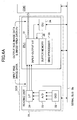
- FIG.4A shows an image data processing system of the color document scanner SCR.
- R, G and B image signals produced by a CCD 22 are converted into 8-bit multivalued R, G and B image data by an A/D converter 23, and are supplied to the IPU1 via an interface (hereinafter referred to as I/F) 24.
- I/F interface
- a main part of the IPU1 is a color image processing unit formed by combining an input-output I/F 31, a buffer memory 32, and an SIMD (Single Instruction Multiple Data) processor (a data processor) 33.
- SIMD Single Instruction Multiple Data
- FIG.5 shows a configuration of the elements of the color image processing unit (31+32+33) of the IPU1.
- the input-output I/F 31 includes image ports 0 to 4 inputting and outputting the image data, a mode setter (a mode designation decoder) exchanging control data, control signals or synchronizing signals, an SCI (Serial Communication Interface), an interruption controller, a JTAG (a job designation decoder/encoder), a host I/F, a clock generator, and a timer.
- the image ports 0 and 1 are used exclusively for inputting the image data.
- the image port 2 is used for inputting and outputting the image data.
- the image ports 3 and 4 are used exclusively for outputting the image data.
- the image ports are capable of inputting and/or outputting 2-byte data simultaneously in parallel, i.e., capable of inputting and/or outputting two series of image data simultaneously in parallel.
- the RGB and YMCK color image data (having multivalued gradation) are 8-bit; also, read data and/or printout data (having multivalued gradation) upon designating a monochrome (black-and-white image) reading and/or a monochrome (black-and-white) printing (upon designating a monochrome-processing/image mode), i.e., black-and-white image data, are 8-bit.
- two items of image data i.e., two-pixel image data
- two items of one-pixel RGB image data can be simultaneously input and/or output in parallel.
- Each of RAMs 8K (8K byte) of the buffer memory 32 has a capacity capable of storing one line of multivalued image data of 600 dpi parallel with a shorter side of an A3 sheet (8-bit: a kind of R, G, B, Y, M, C, K image data), and is used as a line buffer for inputting and/or outputting image data, or is used as an LUT.
- the RAMs 8K total 16, each of which can select reading/writing of two bytes at one time, or reading/writing of one byte at one time.
- Two RAMs 2K are used as a cyclic shift register cyclically shifting the image data so as to absorb a difference in rates of serial data transfer between a source of the image data transfer and a destination of the image data transfer.
- RAMs are connected to one of memory switches SW1 to SW3.
- Memory controllers MECs
- the memory controllers determine ON/OFF of switches inside the memory switches SW1 to SW3 according to an input/output mode designation provided by the SIMD processor 33. That is, upon an image-port/memory-controller/RAM using mode, the memory controllers arrange connections of the memory-switches, the RAMs to be used, and the SIMD-processor 33. Then, the memory controllers perform inputting/outputting (parallel, serial conversions and transfer) of the image data according to the designated mode.
- the memory controller When the designated mode is a writing to the LUT (conversion table), the memory controller writes ⁇ conversion data provided by the SIMD processor 33 at an address designated by the SIMD processor 33 in the RAM 8K (LUT RAM) designated by the SIMD processor 33.
- the memory controller When the designated mode is a reading of input color image data, the memory controller writes color image data supplied via the image port in the RAM 8K (input line buffer) designated by the SIMD processor 33.
- the memory controller When the designated mode is a conversion (e.g., ⁇ conversion) of gradation properties of color image data by using the LUT, the memory controller reads ⁇ conversion data corresponding to input image data by accessing the RAM 8K (LUT RAM) having the LUT, and writes the input image data of the image port or the RAM 8K (input line buffer) designated by the SIMD processor 33 in the SIMD processor 33 or the RAM 8K (output line buffer) designated by the SIMD processor 33.
- the designated mode is a transmitting of color image data
- the memory controller transmits color image data output by the SIMD processor 33 or color image data of the RAM 8K (output line buffer) designated by the SIMD processor 33, to the image port.
- Other designated modes include a mode of writing color image data to the RAM 8K (input line buffer) that performs a parallel/serial conversion or a serial/parallel conversion, and a mode of reading color image data from the RAM 8K (output line buffer).
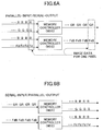
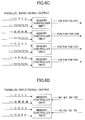
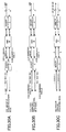
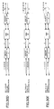
- FIG.6A to FIG.6E show a variety of parallel/serial conversions or serial/parallel conversions of image data performed by the memory controller.
- FIG.6A shows a manner of performing a parallel/serial conversion in which respective R, G and B image data (three series: one series includes one line of image data of one color) and image-area data Fd (one series: one line of image-area data) supplied from the image port, the RAM or the SIMD processor 33 are converted into a total of two series, wherein each of the memory controllers compiles two series into one series.
- the R image data and the G image data input in parallel in two series are converted into one series by an alternate pickup compilation
- the B image data and the image-area data Fd input in parallel in two series are converted into one series by an alternate pickup compilation.
- FIG.6B shows a serial/parallel conversion in which the two series of serial data serial-converted in FIG.6A are returned to the original four series of parallel data.
- FIG.6C shows a parallel/serial conversion performed in a similar buffer memory of the IPU2 upon outputting YMCK image data to the IPU3y, IPU3m, IPU3c and IPU3k, though not performed in the buffer memory 32 of the IPU1.
- five series of parallel data i.e., respective Y, M, C and K image data (four series) and image-area data Fd (one series) are converted into four series of serial data.
- Each of the four series of serial data is transferred to the IPU3y, IPU3m, IPU3c or IPU3k, respectively.
- Each of the IPU3y, IPU3m, IPU3c and IPU3k performs an inverse conversion, i.e., a serial/parallel conversion, so as to divide the one series of serial data into two series of the Y, M, C or K image data and the image-area data Fd.
- an inverse conversion i.e., a serial/parallel conversion
- FIG.6D shows a parallel/serial conversion performed in the similar buffer memory of the IPU2 upon serially outputting parallel YMCK image data generated by an SIMD processor of the IPU2 to the parallel bus Pb, though not performed in the buffer memory 32 of the IPU1.
- four series of the parallel data i.e., respective Y, M, C and K image data (four series) are converted into two series of serial data.
- the IPU2 Upon receiving these two series of serial data, the IPU2 performs an inverse conversion, i.e., a serial/parallel conversion, so as to divide the two series of serial data into the original four series of the Y, M, C and K image data.
- one line of image data is divided into two series, i.e., one series of odd-numbered pixels and the other series of even-numbered pixels (indicated by solid-lined arrows); or, conversely, two series, i.e., image data string of odd-numbered pixels and image data string of even-numbered pixels are compiled into a series of one line (indicated by broken-lined arrows).
- FIG.6E shows the division/compilation of monochrome image data Bk output by the reading unit 21 in a monochrome mode, and the same division/compilation applies to color image data of one color (e.g., R image data; R in place of Bk).
- the SIMD processor 33 includes an input-output port capable of inputting/outputting 2-byte data simultaneously in parallel from/to outside (the memory controllers), which not only can input/output two bytes simultaneously, but also can input/output each of the two bytes individually. Any of the two-byte input/output and the byte-byte input/output can be selected.
- the SIMD processor 33 may include a plurality of input-output ports, each of which can be selectively used for inputting/outputting.
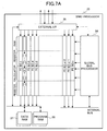
- FIG.7A illustrates an internal structure of the SIMD processor 33 shown in FIG.5.
- FIG.7B illustrates a structure of a part of one of processor elements PE shown in FIG.7A.
- This SIMD processor 33 has local memory RAMs divided according to the processor elements PE, and controls memory areas and data paths, which are to be used, by a data bus control provided in a global bus processor 38. Input data and data to be output are stored in each of the local memory RAMs assigned as buffer memories, and are output to the outside by an external I/F 39.
- the global bus processor 38 provides same operation commands simultaneously to the 320 processor elements PE including the local memory RAMs and applying same image processes to 8-bit-or-more multivalued image data in parallel. An operation result of the processor element PE is stored again in the local memory RAM, and then is output to the memory controller via the external I/F 39.
- a processing procedure for the processor element PE, parameters for the processing and so forth are exchanged between a program RAM 36 and a data RAM 37.
- Programs and data stored in a HDD (which is a storage, e.g., a nonvolatile memory, composing the data conversion device) is downloaded to the program RAM 36 and the data RAM 37 via the IMAC, the parallel bus Pb, the CDIC and the serial bus Sb, according to a command from the system controller 106.
- a DMAC Direct Memory Access Controller
- the process controller 101 controls the course of the data according to a request from the DMAC.
- the selection by the system controller 106 as to the data set transferred from the HDD to the program RAM 36 and the data RAM 37 is changed by instructions from the operation board OPB or the PC.
- the data set of the HDD to be transferred to the program RAM 36 and the data RAM 37 may be changed therefor.
- an image processing function of the color image processing unit (31+32+33) of the IPU1 is determined according to a reading process program written in the program RAM 36 provided in the SIMD processor 33.
- the reading process program applies the CCD inter-line correction, the main-scanning resist adjustment, the shading correction, the dot correction, the vertical stripe correction, and the scanner ⁇ conversion to the input RGB image data in this order. Further, the reading process program performs the image area separation based on the RGB image data having undergone the vertical stripe correction so as to generate the image-area data Fd, and adds the image-area data Fd to the output RGB image data having undergone the reading process correspondingly at a same position on the image, and outputs the data to the CDIC. Also, the reading process program supplies the RGB image data having undergone the vertical stripe correction to an exterior bill recognition unit 34.
- the scanner ⁇ conversion provides RGB image data as a reading address to six of the RAMs 8K of the buffer memory 32 (shown in FIG.5) in which ⁇ conversion LUTs (conversion tables) for the R, G and B image data are formed respectively so as to read ⁇ conversion data corresponding to the provided image data, and supplies the ⁇ conversion data to the SIMD processor 33.
- ⁇ conversion LUTs conversion tables
- ⁇ conversion tables ( ⁇ LUT-Rs) for R image data are written to two of the RAMs 8K; then, the ⁇ LUT-Rs of the RAMs 8K are simultaneously in parallel supplied with odd-numbered R image data and even-numbered R image data provided simultaneously in parallel in two series of R image data string of odd-numbered pixels and R image data string of even-numbered pixels so as to read ⁇ conversion data corresponding to the respective image data, and outputs the ⁇ conversion data simultaneously in parallel to the SIMD processor 33.
- ⁇ conversion tables ( ⁇ LUT-Gs) for G image data are written to other two of the RAMs 8K, and identical ⁇ conversion tables ( ⁇ LUT-Bs) for B image data are written to the other two of the RAMs 8K; then, ⁇ conversions of the G image data and the B image data are performed in the same manner as the ⁇ conversion of the R image data so as to output the ⁇ conversion data to the SIMD processor 33.
- the SIMD processor 33 can accept only 2-byte data ( ⁇ conversion data of two pixels including an even-numbered pixel and an odd-numbered pixel of a same color) simultaneously, the ⁇ conversions of the G image data, the B image data and the R image data are performed according to different timings.
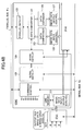
- FIG.4B show a configuration of the CDIC.
- the IPU2 performs the serial/parallel conversion shown in FIG.6B by a memory controller thereof so as to divide the RGB image data (including the image-area data Fd) into the respective R, G and B image data and the image-area data Fd.
- the IPU2 applies the intermediate processes to the RGB image data so as to produce 8-bit multivalued YMCK image data of the respective YMCK recording colors.
- the IPU2 When an output to the parallel bus Pb is designated, the IPU2 performs the parallel/serial conversion shown in FIG.6D, or in hereinafter-described manners (Ef, Ff) shown in FIG.30E and FIG.30F, so as to output the YMCK image data to an image data input control 122 of the CDIC.
- the image data received by the image data input control 122 is subjected to the primary compression by a data compressor 123 so as to enhance a transfer efficiency in the parallel bus Pb.
- the compressed image data is converted into parallel data by a data converter 124, and is transmitted to the parallel bus Pb via a parallel data I/F 125.
- Image data supplied from the parallel bus Pb via the parallel data I/F 125 is converted into serial data by the data converter 124.
- This data which has been subjected to the primary compression for a bus transfer, is expanded by a data expander 126.
- the expanded image data is two series of serial data output from memory controllers shown in FIG.6D, and is transferred to the IPU2 by an image data output control 127.
- the IPU2 performs a serial/parallel conversion so as to divide the two series of serial data into the Y, M, C and K image data.
- the CDIC has functions of converting parallel data transferred by the parallel bus Pb and serial data transferred by the serial bus Sb.
- the system controller 106 transfers data to the parallel bus Pb, and the process controller 101 transfers data to the serial bus Sb.
- the data converter 124 and a serial data I/F 129 convert parallel/serial data conversion for communications on the parallel bus Pb and the serial bus Sb.
- a serial data I/F 128 is an I/F for the IPU2, and transfers serial data to the IPU2.
- FIG.8A shows a configuration of the IPU2.
- the IPU2 is a color image processing unit formed by combining an input-output I/F 41, a buffer memory 42, and an SIMD processor 43.
- This color image processing unit has a similar configuration as the color image processing unit (31+32+33) of the IPU1 shown in FIG.5; however, data and programs stored in a program RAM and a data RAM of the SIMD processor 43 of the IPU2 apply the intermediate processes (a filtering process, a ground-color removal, a color conversion, i.e., a conversion to the YMCK image data, an under-color removal, a main-scanning magnification variation, a main-scan shift, a main-scan mirroring, a sub-scan culling, a masking process, and a binarization upon outputting a monochromatic character) to the RGB image data.
- the intermediate processes a filtering process, a ground-color removal, a color conversion, i.
- FIG.8B shows a configuration of the IMAC.
- a parallel data I/F 141 manages input/output of image data form/to the parallel bus Pb, and controls storing/reading of the image data to/from the MEM, and controls a conversion of code data, which is input mainly from the external personal computer PC, to image data.
- the code data input from the external personal computer PC is stored in a line buffer 142. That is, data is stored in a local area.
- the code data stored in the line buffer 142 is converted into image data in a video control 143 according to a conversion process command supplied from the system controller 106 via a system controller I/F 144.
- the converted image data or the image data supplied from the parallel bus Pb via the parallel data I/F 141 is stored in the MEM.
- a data converter 145 selects image data to be stored;
- a data compressor 146 performs the secondary compression so as to enhance efficiency in using memories;
- a memory access controller 147 stores the compressed data in the MEM while managing addresses in the MEM.
- the memory access controller 147 controls the reading address, and the read image data is expanded in a data expander 148.
- the expanded image data is data of the primary compression performed for being transferred in the parallel bus Pb, and is transmitted via the parallel data I/F 141 to the parallel bus Pb.
- the facsimile control unit FCU shown in FIG.3 which performs FAX transmission/reception, converts image data into a communication format, and transmits the data to the external line PN; conversely, the FCU converts data supplied from the external line PN into image data, and records (outputs) the image data in the image forming unit 105 via an external I/F and the parallel bus Pb.
- the FCU comprises a FAX image process, an image memory, a memory controller, a facsimile controller, an image compression/expansion, a modem, and a network control device.
- An output buffer function of image data is partially aided by the IMAC and the MEM.
- the facsimile controller upon starting to transmit image information, orders the memory controller to read stored image information from the image memory successively.
- the read image information is decoded into the original signal by the FAX image process, and also is subjected to a density conversion process and a magnification varying process, and then is supplied to the facsimile controller.
- the image signal supplied to the facsimile controller is subjected to an encoding compression by the image compression/expansion unit, and is modulated by the modem, and thereafter is transmitted to a destination via the network control device. Then, the transmitted image information is deleted from the image memory.
- a received image is temporarily stored in the image memory in the FCU, and if the received image can be output (recorded) at this point, the received image is output (recorded) upon completion of the reception of images corresponding to one page.
- FIG.9 shows a configuration of the IPU3y, IPU3m, IPU3c and IPU3k.
- the IPU3y, IPU3m, IPU3c and IPU3k have the same configuration, and perform substantially similar output corrections (a printer ⁇ conversion and a gradation process).
- the IPU3y will be described.
- the IPU3y is a color image processing unit formed by combining an input-output I/F 51y, a buffer memory 52y, and an SIMD processor (a data processor) 53y.
- This color image processing unit has a similar configuration as the color image processing unit (31+32+33) of the IPU1 shown in FIG.5; however, data and programs stored in a program RAM and a data RAM of the SIMD processor 53y of the IPU3y apply the printer ⁇ conversion for Y to the Y image data, and further convert the data into binary data for printing, by the gradation process.
- the gradation process includes a density gradation process, a dither process, a random dither binarization, one of which is performed according to an image process mode designation or the image-area data Fd.
- the SIMD processor 53y is connected to a random dither binarization unit 35 shown in FIG.5. In FIG.9, this random dither binarization unit 35 is not shown.
- the IPU3y, IPU3m, IPU3c and IPU3k Upon receiving serial data including image-area data Fd output from memory controllers shown in FIG.6C, the IPU3y, IPU3m, IPU3c and IPU3k perform an inverse conversion of the parallel/ serial conversion shown in FIG.6C, i.e., a serial/parallel conversion shown in FIG.30D (Dr), so as to divide the Y, M, C or K image data and the image-area data Fd.
- the IPU3y parallel-converts one series of serial data including the Y image data and the image-area data Fd alternately into one series of the Y image data and one series of the image-area data Fd.
- the two series of the two-pixel image data are supplied simultaneously to the IPU3y, IPU3m, IPU3c and IPU3k, and are processed simultaneously in parallel therein.
- the two series of the data string of the odd-numbered pixels and the data string of the even-numbered pixels, which are generated by the IPU3y, IPU3m, IPU3c and IPU3k for outputting to the image forming unit 105, are output to the image forming unit 105 after the data of the odd-numbered pixels and the data of the even-numbered pixels are compiled into a image data string of serial data in one series for printing out one line, as indicated by the broken-lined arrows in FIG.6E (or as indicated by direction Bf in FIG.30B).
- FIG.6E shows a case of Bk image data processed by the IPU3k, the same applies to Y, M and C image data processed by the IPU3y, IPU3m and IPU3c.
- the CDIC which is an image data controller
- the IMAC which is an image memory controller
- the SCR, the IPU2, and the PTR which are independent from one another, are not directly connected to the parallel bus Pb but to the CDIC or the IMAC, only the CDIC and the IMAC controls the use of the parallel bus Pb. Therefore, it is easy to control a mediation and a transfer with respect to the parallel bus Pb efficiently.
- FIG.10A and FIG.10B are flowcharts of a process of storing an image in the image memory MEM and an image data process of reading an image from the image memory MEM.
- FIG.10A shows a process of writing RGB image data produced by the SCR, or YMCK image data converted by the IPU2, in the MEM, i.e., transfer processes Ip1 to Ip14.
- FIG.10B shows an image data process of reading image data from the MEM and outputting to the image forming unit 105 of the PTR, or reading RGB image data, converting the RGB image data into YMCK image data by the IPU2, and rewriting the YMCK image data in the MEM, i.e., transfer processes Op1 to Op13.
- the CDIC controls the data flow as above between busses and units.
- the CDIC Upon writing RGB image data produced by the SCR in the MEM, the CDIC selects a route (C) from step Ip4 to step Ip6. Upon printing YMCK image data converted by the IPU2 from RGB image data produced by the SCR, the CDIC selects a route (A) from step Ip4 to step Ip5.
- the CDIC Upon reading from the MEM, the CDIC selects a route (D) from step Op8 to step Op10 when read data is YMCK image data; the CDIC selects a route (E) from step Op8 via Ip5-Ip8 to step Op10 when reading RGB image data, converting the RGB image data into YMCK image data, and rewriting the YMCK image data in the MEM; the CDIC selects a route (F) from step Op8 to step Op9 when reading RGB image data, converting the RGB image data into YMCK image data, and printing the YMCK image data.
- a route (D) from step Op8 to step Op10 when read data is YMCK image data
- the CDIC selects a route (E) from step Op8 via Ip5-Ip8 to step Op10 when reading RGB image data, converting the RGB image data into YMCK image data, and rewriting the YMCK image data in the MEM
- the CDIC selects a route (
- Each of the reading corrections of RGB image data by the IPU1, the intermediate processes including the conversion to YMCK image data by the IPU2, and the output corrections for printing by the IPU3k applies substantially similar image processes to each image data corresponding to each pixel on one line. Specifically, there are processes switching contents of the processes according to differences as to image-area data Fd; even in this case, the processes of the same contents are applied if the image-area data Fd are identical.
- the IPU1 to IPU3 use the SIMD processors 33, 43, 53y, 53m, 53c and 53k to apply same image processes simultaneously in parallel to each of a number of multivalued gradation color image data by a number of the processor elements PE so as to enhance a color image processing rate for the above-mentioned reading corrections, the intermediate processes and the output corrections.
- each of the SIMD processors 33, 43, 53y, 53m, 53c and 53k comprises the 320 processor elements PE each processing 8-bit-or-more multivalued image data so as to process 320 items (320 pixels) of image data simultaneously.
- Matrixes used in the dither process may have sizes of 4 ⁇ 4, 8 ⁇ 8 and 16 ⁇ 16.
- the processor elements PE needs to be provided in number corresponding to integral multiples of 96 (6 ⁇ 16) which is the least common multiple of 6 and 16 because 4 and 8 are divisors of 16.
- a filtering process an MTF correction
- an edge emphasis or a smoothing process to image data of the present pixel
- 16 processor elements need to be allocated as offsets on each side of the 96 ⁇ 3 processor elements PE (effective elements) actually calculate and output operation data; and the respective 16 processor elements need to be supplied with image data of neighboring pixels on both sides of the 96 ⁇ 3 pixels, and need to perform a sum-of-product calculation or a pattern comparison so as to supply the results to the effective elements.
- more than 96 ⁇ 3 processor elements are used in the simultaneous and parallel image processes.
- the number of multivalued gradation data exceeds 312, such as 512, 1024 or 2048, in cases the multivalued gradation data are of 9, 10, 11 or 12 bits, for example, when the number of multivalued gradation data is 512, first multivalued gradation data 0-319 are subjected to interpolative calculations at one time, and calculated ⁇ conversion data are written to LUT RAMs; and next, the remaining multivalued gradation data 320-511 are subjected to interpolative calculations at one time, and calculated ⁇ conversion data are written to LUT RAMs.
- ⁇ conversions by interpolative calculations may be performed separately at a plurality of times.
- the hard disk HDD (shown in FIG.3) includes image processing programs and data to be loaded to the respective program RAMs and the data RAMs (36 and 37 shown in FIG.7) of the SIMD processors 33, 43, 53y, 53m, 53c and 53k.
- the system controller 106 When the system controller 106 performs initial settings for the system in response to a reset signal produced according to the power on, and a reset instruction from the operation board OPB or the host PC, the programs and the data stored in the hard disk HDD for the SIMD processors 33, 43, 53y, 53m, 53c and 53k are loaded to the respective program RAMs and the data RAMs of the SIMD processors 33, 43, 53y, 53m, 53c and 53k by utilizing the above-described data transfer using the IMAC, the parallel bus Pb, the CDIC, the serial bus Sb and the process controller 101.
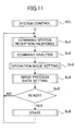
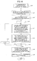
- FIG.11 is a flowchart of system settings of the system controller 106 in response to an image process instruction from the operation board OPB or the host PC.
- the system controller 106 exchanges commands, responses and status information between the OPB, the PC, the FCU, the SCR and the PTR.
- the system controller 106 receives an image processing command (instruction) from the OPB, the PC or the FCU (step Sc1), the system controller 106 analyses the command, i.e., decodes the command data (step Sc2).
- the system controller 106 determines an operation mode of each of the system elements shown in FIG.3 according to the command analysis result (Sc3), and transfers image process data corresponding to the operation mode (Sc4).
- Each of the system elements sets therein the received operation mode and the image process data, and communicates "ready" to the system controller 106 when the execution thereof is possible.
- the system controller 106 orders each of the system elements to commence the image process (Sc6).
- FIG.12 is a flowchart of initial settings of the SIMD processor 33 of the IPU1 in response to an initial-setting instruction of the system controller 106.
- the system controller 106 supplies the SIMD processor 33 with an initial-setting command that includes a transfer source address and a download instruction of the programs and the image process data stored in the hard disk HDD for the SIMD processor 33.
- the DMAC of the external I/F 39 responses to this command, and writes program data at the designated address in the program RAM 36, and writes the image process data (reference data) in the data RAM 37 (step Sd1).
- the SIMD processor 33 Upon completion of this data transfer, in response to a "ready" notice of the DMAC, the SIMD processor 33 performs a setting of the buffer memory 32 (Sd2), a generation of shading correction LUTs (Sd3), a generation of dot correction LUTs (Sd4), a generation of LUTs for R, G and B ⁇ conversions (Sd5), a generation of LUTs for IDU ⁇ conversions (Sd6), and a generation of various LUTs for image-area separation (Sd7), according to an initial-setting program of the program RAM 36. Upon completion of these processes, the SIMD processor 33 provides a "ready" notice.
- the usage allocation of the 16 RAMs 8K and the 2 RAMs shown in FIG.5 is performed according to memory allocations in the initial-setting program.
- Types of the usage include an input line buffer temporarily storing input image data, an output line buffer temporarily storing image data to be output, an intermediate line buffer temporarily storing, image data being processed, an LUT, and a delay memory for data delay or synchronization.
- These settings are realized by the SIMD processor 33 supplying each of the 16 memory controllers shown in FIG.5 with corresponding memory-controller setting information written in a memory-controller setting register provided in the SIMD processor 33.
- An initial information of the memory-controller setting information is read from the data RAM 37 by the SIMD processor 33 according to the initial-setting program, and is written in the memory-controller setting register. Thereafter, when the image process starts, the memory-controller setting information is rewritten as the process proceeds.
- FIG.13A shows segments of the memory-controller setting information on the memory-controller setting register.
- FIG.13B shows main items of the memory-controller setting information.
- the setting information supplied to a memory controller 1 controlling reading/writing of data from/to RAM 8K No.1 designates "line buffer” and "write", as shown in FIG.13C.
- a writing-designated area ranges from a start address to an end address.
- the setting information shown in FIG.13E indicates that one area of RAM 8K No.15 is used as a line buffer for inputting and outputting image data, and another area of the RAM 8K No.15 is used as an LUT.
- each of the RAMs 8K shown in FIG.5 can be not only used as a line buffer or an LUT, but also can be used as a line buffer and an LUT at the same time.
- the line buffer and the LUT are accessed in time division, i.e., are accessed according to different timings.
- FIG.14A to FIG.14F show a variety of manners of using each of the RAMs 8K.
- FIG.14A shows a data reading/writing area of the RAM 8K upon using the RAM 8K as a line buffer memory (an input buffer, an intermediate buffer or an output buffer) for one line of image data parallel with a shorter side of an A3 sheet.
- FIG.14B shows a manner of using the RAM 8K as a line' buffer memory for two lines of image data parallel with a shorter side of an A4 sheet.
- FIG.14C shows a manner of using the RAM 8K as a line buffer memory for one line of the A3 sheet and one LUT.
- FIG.14D shows a manner of using the RAM 8K as one LUT.
- FIG.14E shows a manner of using the RAM 8K as seven LUTs.
- the manner shown in FIG.14E is preferable in a case where seven types of LUTs each for a monochromatic component are prepared, and one is selectively used real-time according to an image-area separation result, or according to a property designation from the OPB or the PC.
- FIG.14F shows a manner of using some of the RAMs 8K as memories for temporarily storing an LUT read from the HDD or an LUT generated by the SIMD processor 33.
- an LUT10, an LUT11 and an LUT12 for RGB ⁇ conversions, respectively are generated by the SIMD processor 33 and stored; when the ⁇ conversions for RGB image data is performed, the LUT10 for R image data is written in other two RAMs 8K, which are used to apply the ⁇ conversions to one series of R image data of odd-numbered pixels and one series of R image data of even-numbered pixels simultaneously in parallel.
- G image data and B image data are used to apply the ⁇ conversions to one series of R image data of odd-numbered pixels and one series of R image data of even-numbered pixels simultaneously in parallel.
- an access mode of "(1/2) odd-number synchronism detection / (1/2) even-number synchronism detection” designates parallel/serial conversions shown in FIG.6A, FIG.6C, FIG.6D, FIG.30A to FIG.30G and so forth, or designates a compilation into one series indicated by the broken-lined arrows in FIG.6E and FIG.30A to FIG.30G.
- a reading-correction program stored in the hard disk drive HDD for the IPU1 includes storage addresses (for example, S1R, S1G and S1B in a first group shown in FIG.15) of scanner ⁇ conversion programs inserted at a location of ⁇ conversion.
- storage addresses for example, S1R, S1G and S1B in a first group shown in FIG.15
- R, G and B scanner ⁇ conversion programs at the storage addresses are replaced with the storage addresses so as to be transferred.
- the programs in the program RAM 36 can be rewritten to programs of other groups shown in FIG.15 (for example, programs at S3R, S3G and S3B) by providing a rewrite command to the system controller 106 by a changing operation (an rewrite order input) from the OPB or the host PC.
- Y, M, C and K output-correction programs stored in the hard disk drive HDD for the IPU3y, IPU3m, IPU3c and IPU3k, respectively, include storage addresses (for example, P1Y, P1M, P1C and P1K in a first group shown in FIG.15) of Y, M, C and K printer ⁇ conversion programs inserted at a location of ⁇ conversion.
- Each gradation data representing 0-255 is subjected to a ⁇ conversion by an interpolative calculation of a linear approximation using numerical expressions representing the resulting lines. The following is the sections to which these interpolative calculation expressions are applied.
- the boundary value is xi (x1-x8), and the interpolative calculation parameters are inclination ai (a1-a8) and y-intercept (offset) bi (b1-b8).
- Each of conversion programs listed in FIG.15 calculates ⁇ -converted output gradation data y corresponding to input gradation data x according to these calculation expressions.
- the numerous conversion programs listed in FIG.15 are different from one another with respect to (parameters governing) linear equations or (boundary values governing) sections, i.e., different with respect to ⁇ conversion properties (gradation conversion properties).
- the gradation data is 8-bit multivalued gradation data.
- the global bus processor (38) writes the data (AD0 to ADn: the calculated Y) stored in the output resisters of the processor elements PE0 to PEn to output data areas of the respective RAMs of the processor elements, and orders the memory controller (shown in FIG.5) designated as conducting reading/writing of ⁇ conversion LUTs by the memory-controller setting register shown in FIG.13A to read the data from the output data areas.
- the memory controller writes the ⁇ conversion data ( ⁇ conversion table) correspondingly to the gradation data representing 0-255, in a designated area in the RAM 8K designated as an LUT by the setting information ( ⁇ p9).
- the processor elements perform only one calculation; thus, a conversion rate is high.
- the image processor (33) has a small number of data processing steps, when a total of 256 items of gradation data representing 0-255 are ⁇ -converted simultaneously by using the 256 processor elements among the 320 processor elements (PE). Compared to a conventional case where the ⁇ conversion of gradation data is repeated 256 times, the number of steps is largely reduced, and a generation rate of ⁇ conversion LUTs is high.
- the above-described ⁇ conversion can be changed by rewriting the scanner ⁇ conversion programs in the reading-correction program written in the program RAM (36) of the SIMD processor 33 of the IPU1, or the printer ⁇ conversion programs in the output-correction programs written in the program RAMs of the SIMD processors of the IPU3y, IPU3m, IPU3c and IPU3k, with other programs stored in the HDD which have different ⁇ conversion properties.
- ⁇ conversion table written in the RAM 8K in step ⁇ p9 in FIG.16 when the ⁇ conversion is performed, one conversion table ( ⁇ LUT-R) is written in the two RAMs 8K, as shown in FIG.18, one of which is allocated for the ⁇ conversion of image data of odd-numbered pixels and the other is allocated for the ⁇ conversion of image data of even-numbered pixels.
- FIG.18 shows the course of data upon the ⁇ conversion of R image data. The same applies to the ⁇ conversions of G image data and B image data.
- one series of R image data of odd-numbered pixels and one series of R image data of even-numbered pixels on the same line, each odd-numbered pixel and each even-numbered pixel being adjacent on an image are supplied to a memory controller via one image port simultaneously in parallel.
- the memory controller provides the first RAM 8K storing the first ⁇ LUT-R with an LUT access address including R image data of the odd-numbered pixel plus a write-start address of the first ⁇ LUT-R as a reading address, and simultaneously in parallel provides the second RAM 8K storing the second ⁇ LUT-R with an LUT access address including R image data of the even-numbered pixel plus a write-start address of the second ⁇ LUT-R as a reading address.
- first ⁇ conversion data data in the first ⁇ LUT-R
- second ⁇ conversion data data in the second ⁇ LUT-R
- the input image data may be stored temporarily in a RAM 8K, and then be supplied to the memory controller.
- the ⁇ conversion data may be stored temporarily in a RAM 8K, and then be output to the SIMD processor 33.
- Hardware according to a second embodiment is the same as in the foregoing first embodiment; however, the second embodiment has different data processes in an interpolative calculation of the ⁇ conversion for generating LUTs.
- FIG.19 is a flowchart of the ⁇ conversion for generating LUTs (a generation of LUTs for a scanner ⁇ conversion in the IPU1, and a generation of LUTs for printer ⁇ conversions in the IPU3y, the IPU3m, the IPU3c and the IPU3k) performed by the IPU1, the IPU3y, the IPU3m, the IPU3c and the IPU3k of the second embodiment.
- the global bus processor (38) provides the boundary value xi of the section i to all of the processor elements PE0 to PEn, and orders a comparison.
- the processor element which sets its flag at "1" (i.e., from “0” to "1") for the first time, writes the calculated value Aj (either of A0 to An) in an output register ADj (step a ⁇ p5).
- the processor element which does not change its flag from "0" to "1", does not perform this writing.
- the global bus processor (38) writes the data (AD0 to ADn) stored in the output resisters of the processor elements PE0 to PEn to the output data areas of the respective RAMs of the processor elements, and orders the memory controller (shown in FIG.5) designated as conducting reading/writing of ⁇ conversion LUTs by the memory-controller setting register shown in FIG.13A to read the data from the output data areas.
- the memory controller writes the ⁇ conversion data correspondingly to the gradation data representing 0-255, in an area designated for LUT formation in the RAM 8K designated as an LUT by the setting information (a ⁇ p8).
- each of the processor elements calculates ⁇ conversion data by performing an interpolative calculation of the same section at the same time.
- gradation data provided for each of the processor elements is not necessarily the same, and is not necessarily in the section i corresponding to the interpolative calculation.
- a calculation output of the processor element provided with gradation data out of the section i is an error, and a calculation output of the processor element provided with gradation data within the section i is correct.
- Hardware according to a third embodiment is the same as in the foregoing first embodiment; however, in the third embodiment, an interpolative calculation program used in a generation of LUTs for ⁇ conversions has a different configuration.
- a description will be given of ⁇ conversions (a generation of LUTs for a scanner ⁇ conversion in the IPU1, and a generation of LUTs for printer ⁇ conversions in the IPU3y, the IPU3m, the IPU3c and the IPU3k) performed by the IPU1, the IPU3y, the IPU3m, the IPU3c and the IPU3k of the third embodiment.
- a reading-correction program for the IPU1 includes a storage address S00 of a scanner ⁇ conversion program inserted at a location of the generation of ⁇ conversion LUTs, as shown in FIG.20.
- the scanner ⁇ conversion program at the storage address S00 is replaced with the storage address so as to be transferred.
- a set of "boundary values, parameters" for R, G and B ⁇ conversions e.g., data at addresses S1R, S1G and S1B shown in FIG.20, is transferred and written to a ⁇ -conversion data storage area of the data RAM 37 of the SIMD processor 33.
- FIG.21 shows information divisions of a group of parameters on the data RAM 37.
- the set in the data RAM 37 can be rewritten to other sets shown in FIG.20 (for example, a set at S3R, S3G and S3B) by a changing operation from the OPB or the host PC.
- each of Y, M, C and K output-correction programs for the IPU3y, IPU3m, IPU3c and IPU3k, respectively, includes a storage address P00 of a ⁇ conversion program inserted at a location of ⁇ conversion, as shown in FIG.20.
- the printer ⁇ conversion programs at the storage address P00 are replaced with the storage address so as to be transferred.
- a set of "boundary values, parameters" for respective Y, M, C and K ⁇ conversions e.g., data at addresses P1Y, P1M, P1C and P1K shown in FIG.20, are transferred and written to ⁇ -conversion data storage areas of the respective data RAMs of the SIMD processors 53y, 53m, 53c and 53k. Even after writing the set to the data RAMs, the set can be rewritten to other sets shown in FIG.20 (for example, a set at P1Y, P1M, P1C and P1K) by a changing operation from the OPB or the host PC.
- a process flow of ⁇ conversion according to the third embodiment is similar to the process flow according to the first embodiment shown in FIG.16.
- the boundary value xi and the parameters a1 and b1 are read from the data RAM (37) of the SIMD processor (33), and are provided to the processor elements PE.
- a small number of parameters can generate a property curve having a predetermined shape.
- Hardware according to a fourth embodiment is the same as in the foregoing first embodiment; however, in the fourth embodiment, ⁇ conversion tables are not generation by an interpolative calculation, but original conversion tables are stored in the HDD.
- a reading-correction program for the IPU1 includes a storage address S00 (FIG.22) of a scanner ⁇ conversion program inserted at a location of the generation of ⁇ conversion LUTs.
- S00 FIG.22
- the scanner ⁇ conversion program at the storage address S00 is replaced with the storage address so as to be transferred.
- a set of R, G and B ⁇ conversion tables e.g., conversion tables at addresses S1R, S1G and S1B (FIG.22), is transferred and written to a ⁇ -conversion table storage area of the data RAM 37 of the SIMD processor 33.
- the SIMD processor 33 Upon ⁇ -converting RGB image data, the SIMD processor 33 reads the ⁇ conversion tables from the data RAM 37, and writes one conversion table in the two RAMs 8K, as shown in FIG.18, so as to ⁇ -convert image data of odd-numbered pixels and image data of even-numbered pixels on one line simultaneously in parallel.
- the set in the data RAM 37 can be rewritten to other sets shown in FIG.22 (for example, a set at S3R, S3G and S3B) by a changing operation from the OPB or the host PC.
- each of Y, M, C and K output-correction programs for the IPU3y, IPU3m, IPU3c and IPU3k, respectively, includes a storage address P00 (FIG.22) of a ⁇ conversion program inserted at a location of ⁇ conversion.
- P00 FIG.22
- the printer ⁇ conversion programs at the storage address P00 are replaced with the storage address so as to be transferred.
- a set of Y, M, C and K ⁇ conversion tables e.g., data at addresses P1Y, P1M, P1C and P1K (FIG.22) are transferred and written to ⁇ -conversion data storage areas of the respective data RAMs of the SIMD processors 53y, 53m, 53c and 53k. Even after writing the set to the data RAMs, the set can be rewritten to other sets shown in FIG.22 (for example, a set at P1Y, P1M, P1C and P1K) by a changing operation from the OPB or the host PC.
- YMCK image data are processed simultaneously in parallel by the four respective SIMD processors 53y, 53m, 53c and 53k.
- printer ⁇ conversions or outputting processes of YMCK image data can be performed as a whole by one SIMD processor successively for each color.
- This adapts to a one-drum type color printer forming images of respective colors successively by one photosensitive unit.
- using the four SIMD processors 53y, 53m, 53c and 53k for YMCK image data, respectively, is preferable for a high-speed printing because the outputting processes of YMCK image data as a whole become fast.
- the image-area separation described herein is based on RGB image data, and judges whether an image represented by the RGB image data is a character area (an area of a character or a line), or a picture area (an area of a photograph or a picture, and a non-character area), and produces a C/P signal and a B/C signal.
- the C/P signal represent a character-edge area, a character-inside area, or a picture area.
- the B/C signal represents a chromatic (color) area or an achromatic (blank) area.
- the "character-inside" means within the character edges, i.e., within a width of a character line.
- a combination of 3-bit signals of the C/P signal and the B/C signal is the image-area data Fd.
- the C/P signal is a 2-bit signal: two bits of "11” meaning “3" represents the character-edge area; two bits of "01” meaning “1” represents the character-inside area; and two bits of "00” meaning "0" represents the picture area.
- the B/C signal is a 1-bit signal: H ("1") represents the achromatic (blank) area; and L (“0") represents the chromatic (color) area.
- the image-area separation mainly comprises an MTF correction 321, an edge separation 322, a white-background separation 323, a dot separation 324, a hue separation 325a, a color judgment 325b, and a comprehensive judgment 326.
- a reading density by the reading unit 21 of the scanner SCR is approximately 600 dpi, for example.
- the MTF correction 321 corrects G image data produced by the reading unit 21 mainly for extracting an edge of a character. At this point, since data read by the reading unit 21 is sometimes blurred depending on a capability of the lenses, the data is subjected to an edge emphasizing filter.
- a pixel matrix of the MTF correction 321 contains seven pixels in a main scanning direction x times five pixels in a sub scanning direction y.
- the data RAM 37 (a reference data storage) includes a coefficient group (a coefficient matrix) A and B containing weighing coefficients a1 to a7, b1 to b7, c1 to c7, d1 to d7 and e1 to e7 corresponding to the respective pixels.
- a coefficient of a pixel at the center of a third transverse row in the coefficient matrix, i.e., of a present pixel (a subject pixel), is c4.
- a total sum (a sum of products) (7 times 5 totaling 35 products) obtained by multiplying the coefficients in the coefficient matrix by respective values represented by the image data of respective pixels corresponding to the coefficients is supplied to the edge separation 322, the white-background separation 323, and the dot separation 324, as a image data value processed in the MTF correction 321.
- the present pixel means a pixel being processed at present, which is updated to another pixel successively in the direction x and the direction y.
- a character area includes a multitude of pixels of a high-level density and pixels of a low-level density (hereinafter referred to as black pixels and white pixels, respectively). Additionally, in an edge part of the character area, the black pixels and the white pixels are continuous.
- the edge separation 322 detects a character edge according to continuity of the black pixels and the white pixels.
- the image data subjected to the MTF correction is converted into a ternary value by using two threshold values TH1 and TH2.
- the input data When input data ⁇ TH1, the input data is converted into 2-bit ternary data representing a pixel corresponding to the input data as a white pixel.
- the input data When TH1 ⁇ input data ⁇ TH2, the input data is converted into the 2-bit ternary data representing the pixel corresponding to the input 'data as a middle-tone pixel.
- the input data When TH2 ⁇ input data, the input data is converted into the 2-bit ternary data representing the pixel corresponding to the input data as a black pixel.
- the ternary data is made binary so as to obtain pixel information data representing the presence/absence of an image component ("1" indicating an image component present; "0" indicating an image component absent). Based on this binary data, a part where the black pixels are continuous, and a part where the white pixels are continuous are detected, respectively, by respective pattern matching judgments.
- Examples representing reference patterns used in the black-pixel continuity detection are 3 ⁇ 3 pixel matrixes BPa to BPd shown in FIG.25A.
- 3 ⁇ 3 pixel matrixes BPa to BPd In each of the 3 ⁇ 3 pixel matrixes BPa to BPd, three pixels aligned vertically (y), horizontally (x) and obliquely including at least a present pixel (a central pixel) have pixel information data of "1".
- all of other patterns satisfying this condition are reference patterns used in the black-pixel continuity detection.
- these reference patterns are referred to as black-pixel continuity detection reference patterns.
- Examples representing reference patterns used in the white-pixel continuity detection are 3 ⁇ 3 pixel matrixes WPa to WPd shown in FIG.25A.
- 3 ⁇ 3 pixel matrixes WPa to WPd In each of the 3 ⁇ 3 pixel matrixes WPa to WPd, three pixels aligned vertically (y), horizontally (x) and obliquely including at least a present pixel have pixel information data of "0".
- all of other patterns satisfying this condition are reference patterns used in the white-pixel continuity detection.
- these reference patterns are referred to as white-pixel continuity detection reference patterns.
- a black circle in a pixel indicates that the pixel information data of the pixel is "1" (an image component present), and a white circle in a pixel indicates that the pixel information data of the pixel is "0" (an image component absent).
- the central pixel in each of the 3 ⁇ 3 pixel matrixes is the present pixel.
- the black-pixel continuity and the white-pixel continuity contradict. Therefore, first, in the black-pixel continuity detection, it is checked whether or not pixel information data of pixels in a 3 ⁇ 3 pixel matrix (a-i in FIG.25B) with a present pixel being at the center thereof matches either of the black-pixel continuity detection reference patterns while switching the reference patterns.
- the present pixel is provided with judgment data indicating that the present pixel is a pixel of "black-pixel continuity" ("11": black-continuity pixel).
- the present pixel is provided with judgment data indicating that the present pixel is a pixel of "white-pixel continuity" ("01": white-continuity pixel).
- the present pixel is provided with judgment data ("00") indicating that the present pixel is a pixel of neither "black-pixel continuity” nor "white-pixel continuity".
- the data RAM 37 contains groups of reference data of the black-pixel continuity detection reference patterns and the white-pixel continuity detection reference patterns.
- One reference data includes two groups of reference-pattern pixel-information (9-bit) data arranged serially so as to form 2-byte data, as shown in FIG.25C, for example, in which pixel information data a-i is of a reference pattern (e.g., Bpa).
- the pixel information data items a-i of the present (subject) 3 ⁇ 3 pixel matrix shown in FIG.25B are converted into 2-byte subject data, in which the eight pixel information data items a-h form a first byte, and the remaining pixel information data item i forms a first bit of a second byte, with remaining seven bits of the second byte provided with "0" indicating no image component, as shown in FIG.25C.
- the nine pixel information data items of the 3 ⁇ 3 pixel reference matrix (pattern) are prepared as 2-byte data. In this case, it is judged whether or not the first byte of the subject data matches the first byte of the reference data.
- pixel information data items a-y thereof are converted into 4-byte subject data, in which the 24 pixel information data items a-x form first to third bytes, and the remaining pixel information data item y forms a first bit of a fourth byte, with remaining seven bits of the fourth byte provided with "0" indicating no image component,' as shown in FIG.25E.
- reference data is prepared as similar 4-byte data.
- FIG.24 is a flowchart of a judgment, i.e., a pattern matching PMP, performed by the SIMD processor 33, of whether or not a pixel matrix with each pixel on one line being at the center thereof matches a reference matrix.
- a judgment i.e., a pattern matching PMP
- the SIMD processor 33 provides the buffer memory 32 with input line buffers for storing ternary data of three lines or more, and also provides the buffer memory 32 'with judgment-result line buffers for storing the above-mentioned judgment data ("11": black-continuity pixel / "01”: white-continuity pixel / "00": unmatched) corresponding to each pixel in the center line of the three lines.
- the SIMD processor 33 orders the memory controllers of the buffer memory 32 to transfer the number (A) of items of the data (pm2).
- the memory controller converts pixel information data of each pixel matrix centered around each of present pixels (A in number) aligned in series on the center line (the present line) stored in the input line buffer into a-byte data in the manner shown in FIG.25C on an individual matrix basis, and transfers the a-byte data to the SIMD processor 33.
- the global bus processor 38 of the SIMD processor 33 writes the first a-byte data to the last a-byte data in order in the RAMs of the processor elements (A in number) (pm3).
- the memory controller of the buffer memory 32 writes the pixel information data binarized from the foregoing ternary data in three RAMs 8K allocated as line buffer memories. Then, the memory controller reads pixel information data corresponding to the 3 ⁇ 3 pixel matrix consisting of pixels a-i in which the present pixel e is surrounded by one pixel each in two-dimensional direction (x, y), as shown in FIG.25B. Then, the memory controller converts the pixel information data into 2-byte data in one line as shown in FIG.25C, and supplies the 2-byte data to the SIMD processor 33. Subsequently, the memory controller repeats this process A times, with shifting the present pixel one by one on the same line.
- the global bus processor 38 of the SIMD processor 33 writes each 2-byte data in the RAMs of the processor elements (pm3).
- each of the processor elements writes "00: unmatched” in its output register (pm4).
- the processor element checks whether or not reference data of type i (No. i) stored in the RAM matches the 2-byte data byte by byte (pm5, pm6). When the reference data matches the 2-byte data, the processor element overwrites "11" (for the black-pixel continuity detection reference patterns) or "01" (for the white-pixel continuity detection reference patterns) in the output register (pm7). When the reference data does not match the 2-byte data, the processor element writes nothing. This match/non-match judgment is repeated with switching the reference data groups (the reference patterns) (pm8, pm9). Upon finishing comparisons of all of the groups of the reference data contained in the data RAM 37 with the foregoing 2-byte data, the comparison operation SIMDop is completed.
- the data in the output register represents whether or not a pixel matrix image represented by the foregoing 2-byte data stored in the RAM of the processor element matches the reference patterns (the black-pixel continuity detection reference patterns or the white-pixel continuity detection reference patterns) represented by the reference data.
- the global bus processor 38 of the SIMD processor 33 transfers the data in the output registers of the processor elements (A in number) to the judgment-result line buffers via the memory controllers (pm10). Then, it is checked whether or not the above-described pattern matching is completed to all of the pixels on one line (pm11). When the pattern matching is not completed, next present pixels on the same line are designated as pixels to be subjected to the pattern comparison, and the pattern matching of the foregoing steps starting from pm3 is performed similarly.
- C represents the number of pixels in one matrix in the main scanning direction x
- D represents the number of pixels in one matrix in the sub scanning direction y
- FIG.26 is a flowchart of a data process FED of an edge/non-edge area judgment performed by the memory controller.
- FIG.27A shows an internal feedback loop in the memory controller upon this edge/non-edge area judgment.
- the global bus processor 38 of the SIMD processor 33 reads an edge/non-edge area judgment LUT from the data RAM, and transfers the LUT to the RAM 8K via the memory controller.
- This RAM 8K is referred to as an edge/non-edge judgment RAM 8K (LUT).
- the memory controller receives an LUT address Lad (input data to be converted) from the SIMD processor 33 in an input register 75, and supplies the LUT address Lad to an address line of the RAM 8K (LUT) via a multiplexer 76, an output register 72, and a memory switch SW.
- the memory controller receives an LUT storage data (output converted data) from the SIMD processor 33 in an input-output register 74, and supplies the LUT storage data to an data line of the RAM 8K (LUT) via an input-output register 73 and the memory switch SW, i.e., writes the LUT storage data in the RAM 8K (LUT).
- the global bus processor 38 examines, by using this RAM 8K (LUT) and the memory controller, whether or not a black-continuity pixel or a white-continuity pixel exists in the vicinity of a present pixel so as to judge which of an edge area or a non-edge area the present pixel exists in.
- the block when one or more black-continuity pixel and one or more white-continuity pixel exist within a block consisting of a 5 ⁇ 5 pixel matrix, the block is judged to be an edge area, and a present pixel that is a center pixel of the matrix is provided with information indicating "edge area"; otherwise, the block is judged to be a non-edge area, and the present pixel is provided with information' indicating "non-edge area".
- the memory controller defines an LUT (RAM 8K (LUT)) and line memories (RAMs 8K (LINE)) for five lines or more in the buffer memory 32 as shown in FIG.27A (fe1).
- the memory controller stores detection results of the above-described black-pixel continuity detection and the white-pixel continuity detection for five lines or more in the line memories (RAMs 8K (LINE)), and regards the third (middle) line of the five lines as a present line, and regards each pixel on the present line as a present pixel successively (fe2).
- the memory controller retrieves the foregoing detection results as to each of 5-pixel rows of a 5 ⁇ 5 pixel matrix having a present pixel at the center thereof via an input-output register 71 by supplying a reading address Pad to an address line of the RAMs 8K (LINE) via a multiplexer 77, the output register 72, and the memory switch SW.
- the memory controller judges the present pixel to be an edge area, and generates edge/non-edge information eds (fe3-fe6).
- the memory controller (an image-area judgment unit) supplies this edge/non-edge information eds of the present pixel, decided edge/non-edge information Edp (data in the input-output register 74) of a preceding pixel preceding the present pixel by one pixel in the main scanning direction x, and a detection result Tpd of the above-described black-pixel continuity detection and the white-pixel continuity detection, which is image process data of the present pixel, to the RAM 8K (LUT) as an LUT access address via the input register 75 the multiplexer 76, and the output register 72 (fe7) so as to read decided edge/non-edge information Eds corresponding to a combination of the eds, the Edp and the Tpd from the edge/non-edge judgment RAM 8K (LUT) (fe8).
- the memory controller writes the decided edge/non-edge information Eds in the input-output register 74, and supplies the decided edge/non-edge information Eds (the overwritten decided edge/non-edge information Edp) to the SIMD processor 33 (fe9, fe10). Then, the memory controller checks whether or not the above-described edge/non-edge judgment is completed to all of the pixels on one line (fe11). When the edge/non-edge judgment is not completed, a next pixel on the same line is regarded as a present pixel, and the process of the foregoing steps starting from fe3 is performed similarly.
- the decided edge/non-edge information Edp of the preceding pixel is feedback information.
- the edge/non-edge judgment of the RAM 8K (LUT) is as follows. When the edge/non-edge information eds of the present pixel indicates "edge" (one or more black-continuity pixel and one or more white-continuity pixel exist within the 5 ⁇ 5 pixel matrix), the decided edge/non-edge information Eds is caused to indicate "edge".
- the decided edge/non-edge information Eds is caused to indicate “edge” if the decided edge/non-edge information Edp of the preceding pixel indicates “edge” and the detection result Tpd of the above-described black-pixel continuity detection and the white-pixel continuity detection as to the present pixel indicates "black-pixel continuity” or "white-pixel continuity”.
- the decided edge/non-edge information Eds is caused to indicate "non-edge” if the Edp indicates "edge” and the detection result Tpd indicates "black-pixel continuity" nor "white-pixel continuity”.
- the decided edge/non-edge information Eds is caused to indicate “edge” if the Edp indicates “non-edge” and the detection result Tpd as to the present pixel indicates only "black-pixel continuity”. Otherwise, the decided edge/non-edge information Eds is caused to indicate "non-edge”.
- edge/non-edge judgment LUT prevents an edge/non-edge oscillation from occurring frequently at short intervals so that the edge/non-edge detection is performed more reliably.
- the feedback LUT process using the input register 75 and the multiplexer 76 is not necessarily performed by retrieving data from several RAMs 8K (LINE) to the memory controller, generating an LUT access data (input data) and accessing the LUTs, as shown in FIG.27A, but also performed in a manner of providing the memory controller with one or more sets of data from the SIMD processor 33 and generating the LUT access data.
- FIG.27B shows an internal feedback loop in the memory controller, in which this manner is applied to the above-described edge/non-edge area judgment.
- another memory controller supplies detection results of the black-pixel continuity detection and the white-pixel continuity detection as to the 5 ⁇ 5 pixel matrix from five RAMs 8K (LINE) not shown in FIG.27B to the SIMD processor 33.
- the SIMD processor 33 judges the present pixel to be an edge area, and supplies this edge/non-edge information eds of the present pixel and the detection result Tpd of the black-pixel continuity detection and the white-pixel continuity detection as to the present pixel to the memory controller shown in FIG.27B.
- This memory controller writes these eds and Tpd together with the decided edge/non-edge information Edp of the preceding pixel in the output register 72 via the multiplexer 76, and outputs the eds, the Tpd and the Edp to the RAM 8K (LUT).
- This feedback LUT process improves a state transition processing ability of the SIMD processor.
- an isolated-point elimination corrects an isolated edge to a non-edge area. Then, a pixel judged to be an edge area is provided with edge information valued "1" (indicating an edge area), and a pixel judged to be a non-edge area is provided with edge information valued "0" (indicating a non-edge area).
- an RGB white extraction, a white judgment, a white pattern matching, a black judgment, a black pattern matching, a white correction, and so forth are performed.
- the above-described pattern-matrix data is arranged in a row by the memory controller, and is compared with reference-pattern serial data by a plurality of the processor elements PE so as to perform a matching (a judgment of whether or not the patterns coincide) for one matrix at a time.
- a white-ground area is detected by using image data of R, G and B so as to activate an operation of a white background separation, i.e., to start a process of a white background separation.
- a present pixel a central pixel in the 3 ⁇ 3 pixel matrix
- a white area so as to activate the white pattern matching.
- a virtual white pixel is determined.
- B image data equal to or smaller than a threshold value thwc exists in a 5 ⁇ 5 pixel matrix having a present pixel at the center thereof the present pixel is judged to be a virtual white pixel. Since the hereinafter-described white judgment is based only on G image data, yellow (Y), which cannot be detected according to the G image data, is detected according to the B image data.
- a valley-like white pixel in a small white area which cannot be detected in the above-described RGB white ground detection is detected according to 5 ⁇ 5 pixel matrix distributions RDPa and RDPb of G image data shown in FIG.28B. Specifically, That a minimum density miny among pixels marked with black circles in the 5 ⁇ 5 pixel matrix distribution RDPa is extracted. Then, a maximum density maxy among pixels marked with white circles in the 5 ⁇ 5 pixel matrix distribution RDPa is extracted. Then, a minimum density mint among pixels marked with black circles in the other 5 ⁇ 5 pixel matrix distribution RDPb shown is extracted.
- a maximum density maxt among pixels marked with white circles in the 5 ⁇ 5 pixel matrix distribution RDPb is extracted.
- either of (miny-maxy) and (mint-maxt) that is a positive value larger than the other is determined to be a valley. detection value OUT.
- this valley detection value OUT is equal to or larger than a predetermined threshold value, a present pixel (a central pixel of the 5 ⁇ 5 pixel matrix distribution RDPa or RDPb) is detected as a valley-like white pixel.
- a valley-like state of an image is detected so as to compensate for a white area that cannot be easily detected in the RGB white ground detection.
- State variables MS and SS[I] used in a white judgment are generated and updated.
- the state variable MS is associated with a pixel in a present line (a line being processed).
- the state variable SS[I] is associated with a pixel in a preceding line (a processed line) preceding the present line by one line.
- Each of the state variables MS and SS[I] is 4-bit white-ground information representing a degree of white of a white ground.
- a maximum value assumed by each of the state variables MS and SS[I] is determined at 15, which means a whitest degree.
- a minimum value of each of the state variables MS and SS[I] is 0.
- each of the state variables MS and SS[I] is data representing a degree of white; as each of the state variables MS and SS[I] assumes a larger value, the value means a more intense white.
- both the state variables MS and SS[I] are initialized to 0.
- the white-ground information SS of pixels before the main scanning position of the present pixel in the line one line before the present pixel are updated to values obtained by reducing the white-ground information MS of the present pixel by a reduction rate decreasing by 1 for each one pixel shifted in the main scanning direction x so that the white-ground information MS of the present pixel is propagated at the above-mentioned reduction rate toward a direction opposite the main scanning direction x in the line one line before the present pixel (a white propagation process).
- this white propagation process applies to a case where the white-ground information SS one line before the present pixel is smaller than the white-ground information MS of the present pixel. For example, when a pixel one line before the present pixel is detected as a white ground (a white area) in the RGB white ground detection, the white-ground information of the pixel one line before the present pixel is the maximum value of 15, thus is not updated.
- the white-ground information SS one line before is retained in the RAM 8K, and the internal feedback loop is formed in the memory controller as shown in FIG.27B.
- Either of data (Edp) read from the RAM 8K (the RAM 8K (LUT) shown in FIG.27B) and white propagation process data calculated by the SIMD processor 33 and supplied to the memory controller is selected by the multiplexers 76 and 77 according to a select designation of the SIMD processor 33, and is re-written in the address of the read data (Edp) in the. above-mentioned RAM 8K.
- the white-ground information MS corresponding to the present pixel is increased by 1.
- the white-ground information MS is updated to a value one degree larger in white intensity.
- the maximum value (max) of the white-ground information MS is determined as 15; accordingly, when the white-ground information MS would become larger than 15, the white-ground information MS is caused to stay 15. In this course, the foregoing white propagation process is also performed.
- the white-ground information MS of the present pixel is smaller than the threshold value thw1 (13) and is equal to or larger than a threshold value thw2 (1), and the present pixel is a valley-like white pixel, the state variable MS is maintained at the current value. In this course, the foregoing white propagation process is also performed.
- the white-ground information MS of the present pixel is decreased by 1.
- the white-ground information MS is updated to white-ground information one degree smaller in white intensity.
- the minimum value (MIN) of the white-ground information MS is 0; accordingly, when the white-ground information MS would become smaller than 0, the white-ground information MS is caused to stay 0. In this course, the foregoing white propagation process is also performed.
- a pixel (referred to as a dot-peak pixel) composing a part of halftone dots from pixel density information within a two-dimensional local area having a predetermined size.
- a central pixel within the area is detected as the dot-peak pixel.
- the central pixel has a maximum (mountain-peak) density level or a minimum (valley-peak) density level within the local area.
- Condition 2 An absolute value of a difference between an average of density levels of each pair of pixels symmetric with respect to the central pixel and the density level of the central pixel is equal to or larger than a threshold value Th.
- Mountain/valley-dot-peak pixels are counted on the basis of an individual two-dimensional small area having a predetermined size, and a total of the mountain/valley-dot-peak pixels is determined as a discrete value P of the individual small area.
- this discrete value P is larger than a threshold value Pth, all pixels in the small area (or only the central pixel in the small area, in a process on an individual pixel basis) are judged to be as a dot area.
- Input data of R, G and B are converted into signals of c, m, y, and color-judgment w (white).
- An example of a hue separation is as follows: boundaries of the respective colors are obtained; an RGB difference is defined as a difference between a maximum value and a minimum value of image data of R, G and B in one pixel; a hue dimension is divided into seven areas; and it is judged which of the seven areas the input data belongs to.
- Output signals are 3-bit data comprising one bit for each of c, m and y, and 1-bit data for w of a color pixel detection for a color judgment.
- Threshold values are varied according to the hues so as to select a threshold value corresponding to each of the hue areas when the hue areas have different chromatic ranges.
- This hue separation is an example; thus, whatever operational expressions may be used.
- the outputs c, m, y and w of the hue separation 325a are stored in the buffer memory 32 for five lines, and are used for a color-pixel judgment.
- This correction enlarges a white level of a 5 ⁇ 5 pixel matrix including the present pixel as a central pixel thereof.
- a pattern matching using colored-fine-line patterns of 5 ⁇ 5 pixel matrixes it is detected whether or not the present pixel is a color-line pixel surrounded by white.
- a pattern matching using white-area patterns of 5 ⁇ 5 pixel matrixes it is detected whether or not the present pixel is a white-area pixel. Based on the above-obtained pattern matching results, a color pixel surrounded by a white area is considered to be a color-pixel candidate; when a white area exists otherwise, the present pixel is not considered to be a color pixel.
- the pixel matrix matches color-pixel patterns including no white area the present pixel becomes a color-pixel candidate.
- the numbers of c, m and y being 1 are counted with respect to each of the pixels in the pixel matrix.
- a difference between a maximum value and a minimum value of a counted value with respect to each of c, m and y is equal to or larger than a threshold value thcnt, and the minimum value is smaller than a threshold value thmin, the present pixel is considered to be a color-pixel candidate 1.
- the threshold values thcnt and thmin are determined prior to a copying (process). By performing a plane expansion to y, m and c, and counting the numbers on an individual plane basis in an N ⁇ N matrix, a minimum value is assumed to be black.
- a black pixel fails to be read, a correction thereof becomes possible. Additionally, a chromatic pixel is judged from the difference between the maximum value and the minimum value. Accordingly, a pixel failed to be read as a black pixel can be corrected, and a chromatic pixel is extracted.
- predetermined chromatic pixels exist in the 5 ⁇ 5 pixel matrix including the present pixel at the center, the present pixel is considered to be a chromatic pixel.
- the present pixel is considered to be the color-pixel candidate 1 and the color-pixel candidate 2
- the present pixel is judged to be a color pixel 1.
- the numbers of c, m and y being 1 are counted with respect to each of the pixels in the pixel matrix; whether a color pixel 2 or a color pixel 3 is detected according to a difference between a maximum value and a minimum value of a counted value; and other processes including a blocking process and an isolated-block elimination are performed. Further, it is judged by a pattern matching whether the present pixel is a black-pixel candidate 1 and/or a black-pixel candidate 2. When the present pixel is the black-pixel candidate 1 and the black-pixel candidate 2, the present pixel is judged to be a black pixel.
- the 4 ⁇ 4 pixel matrix as a whole is blocked into a black-pixel block.
- data is output in units of blocks, in which the 4 ⁇ 4 pixels form one block.
- the present block is the black-pixel block, and when peripheral pixels thereof are non-black pixels, the present block is judged to be a non-black-pixel block.
- the present block is judged to be the color pixel 2 by the color-pixel judgment, and is not judged to be the black pixel by the achromatic judgment, the present block is judged to be a color block. Also, when the present block is judged to be a color pixel 3 by the color-pixel judgment, the present block is judged to be color a color block. For the purpose of considering small characters as being continuous with respect to the block judged to be color by the comprehensive color-pixel judgment, when at least one color block exists in a matrix of 9 ⁇ 9 blocks including the present block at the center thereof, the present block is considered to be the color block. This expansion is performed so as to fill up a gap between characters.
- the document is a color document or whether the document is a monochrome document by checking a continuity in a color-pixel block. Specifically, by counting a number of continuous color pixels in the output data (the color-pixel block) of the foregoing expansion, it is judged whether or not the document is a color document.
- the present pixel exists in the color-pixel block, numbers of continuous color pixels with respect to upper-left, upper, upper-right and left pixels of the present pixel are referred to so as to calculate the number of continuous color pixels with respect to the present pixel.
- the present pixel is, for example, a pixel c3 in a 5 ⁇ 5 pixel distribution pattern MPp shown in FIG.28B
- those upper-left, upper, upper-right and left pixels are pixels b2, b3, b4 and c2, respectively.
- the present pixel does not exist in the color-pixel block, the number of continuous color pixels with respect to the present pixel is valued 0.
- an LUT containing correspondences between the number of continuous color pixels of the present pixel (c3) and the numbers of continuous color pixels of the upper-left, upper, upper-right and left pixels b2, b3, b4 and c2 is read from the data RAM 37 of the SIMD processor 33, is written to the RAM 8K (LUT) shown in FIG.28A.
- a feedback loop is formed in a memory controller as shown in FIG.28A.
- Data c2 (the number of continuous color pixels of the left pixel c2) read from the RAM 8K (LUT) and the numbers of continuous color pixels of the upper-left, upper and upper-right pixels b2, b3 and b4 (data b2, b3 and b4) read from the RAM 8K (LINE) storing numbers of continuous color pixels of pixels in a preceding line are combined by the multiplexers 76 and 77 and the output register 72, and are supplied as an LUT access address to the address line of the RAM 8K (LUT) via the memory switch SW so as to read data c3 from the LUT and determine the data c3 to be the number of continuous color pixels of the present pixel (c3).
- the number of continuous color pixels with respect to the present pixel is valued 0.
- a number of continuous color pixels with respect to the upper pixel (b3) of the present pixel (c3) is checked.
- a reference value A is provided with a number of continuous color pixels with respect to the upper-right pixel (b4) plus 1.
- the reference value A is provided with the number of continuous color pixels with respect to the upper-right pixel (b4).
- a reference value B is provided with a number of continuous color pixels with respect to the upper-left pixel (b2) plus 1
- a reference value C is provided with the number of continuous color pixels with respect to the upper pixel (b3) plus 1
- a reference value D is provided with a number of continuous color pixels with respect to the left pixel (c2) plus 1.
- a maximum value among the reference values A, B, C and D is determined to be the number of continuous color pixels with respect to the present pixel (c3).
- the number of continuous color pixels with respect to the upper pixel (b3) is not 0, the number of continuous color pixels with respect to the upper pixel (b3) is provided for the present pixel (c3).
- the document After the number of continuous color pixels with respect to the present pixel (c3) is determined as described above, it is checked whether or not this number of continuous color pixels is equal to or larger than a predetermined value THACS. When this number is equal to or larger than the predetermined value THACS, the document is determined to be a color document, and the process of the continuity counting ends. When the number of continuous color pixels is smaller than the predetermined value THACS, the present pixel is updated to a next pixel in the scanning directions x and y, and the heretofore-described process is repeated. Upon completing the above-described process for all pixels throughout the document, and still, when the number of continuous color pixels is smaller than the predetermined value THACS, the document is determined to be a monochrome image.
- the above-mentioned number of continuous color pixels is substantially a sum of a number of longitudinal colored line segments and a number of transverse colored line segments.
- the number of continuous color pixels with respect to the upper-right pixel is treated differently so as to prevent a duplicate count.
- the comprehensive judgment 326 comprises a character judgment, an expansion process, and a character-inside judgment.
- the present area is judged to be a character edge; otherwise, the present area is judged to be a non-character-edge (a picture or a character-inside).
- the expansion process conducts an expansion to four blocks by performing an OR process of 8 ⁇ 8 blocks, and thereafter performing an AND process of 3 ⁇ 3 blocks, with respect to the result of the character judgment. Specifically, when either of the 8 ⁇ 8 blocks including the present block at the center thereof is a character edge, the present block is also assumed to be a character-edge block. Then, when all of the 3 ⁇ 3 blocks including the present block at the center thereof are character edges, the present block is determined to be a character-edge, and further a total of four blocks including the present block and adjacent three blocks thereof are determined to be character edges.
- the AND process is performed after the OR process because of the following reason.
- the results of the edge separation 322, the white-background separation 323, the dot separation 324, the color judgment 325b, and the character judgment are used so as to generate a character-inside signal representing either of a character-inside area (within a line width).
- Processes and signals used for generating the character-inside signal are as follows.
- Character-inside character signal an OR process of 5 ⁇ 5 blocks is performed for an output signal representing a character-edge/non-character-edge result of the character judgment.
- the output of this OR process is referred to as a character-inside character signal.
- White-block black character signal A when the character-inside character signal is active (a character edge), the output of the white correction of the white-background separation 323 indicates "white correction data present", the result of the color judgment 325b is non-active (achromatic: black-pixel block), the white-block black character signal A is made active (indicating a white-block black character).
- a black character surrounded by white grounds is highly likely to be a character.
- High-density black-area signal B when an OR of 3 ⁇ 3 blocks in a black blocking process of the white-background separation 323 is active (black), the result of the color judgment 325b is non-active (achromatic), the result of the dot separation 324 is non-active (non-dot), and further, the character-inside character signal is non-active (non-character edge), the high-density black-area signal B is made active (indicating a high-density black area). Inside a black character, the character-inside judgment is performed in combination of other conditions because a density therein is high.
- Black-character signal C when the character-inside character signal is active (a character edge), and the result of the color judgment 325b is non-active (achromatic), the black-character signal C becomes active (indicating a black character).
- This active black-character part is likely to be a character edge, in the vicinity of which a character-inside is likely to exist.
- a first digit "2" of a two-digit number of each symbol represents a present line y2, and a first digit "1" thereof represents a preceding line y1 one line before the present line y2.
- a second digit of the two-digit number of each symbol represents a pixel position x on each line.
- the present pixel is judged (determined) to be a character-inside candidate. That is, the character-inside judgment is triggered by the condition that the white-block black character signals A (active) continuously exist.
- a black character surrounded by white grounds (the white-block black character signal A being active) is highly likely to be a character.
- the white-block black character signals A (active) continuously exist because substantially all of the pixels are characters.
- the black-character signal C indicates a high likelihood of a character edge, in the vicinity of which a "character-inside" is likely to exist. Therefore, the character-inside candidate (Q24: active) is judged as described above.
- the character-inside signal is generated from the character-inside candidate (signal Q: active).
- the character-inside signal is judged to be "character-inside signal present" (character-inside signal: active) when a character-edge signal is not present and a character-inside candidate is present.
- the C/P signal is output as follows.
- C/P signal Character-edge signal Character-inside candidate Area judgment 0 Absent Absent Picture area 1 Absent Present Character-inside area 2 - - - 3 Present ⁇ Character-edge area
- 3-bit signals including this 2-bit C/P signal plus the 1-bit B/C signal is the image-area data Fd.
- the image-area data Fd is referred to in the filtering process and the under-color removal performed in the IPU2, and is referred to in the ⁇ conversion and the gradation process performed in the IPU3y, IPU3m, IPU3c and IPU3k.
- the filtering process performed in the IPU2 is a filtering process for applying an MTF correction to RGB data.
- a weighted average value is obtained by multiplying each of the' coefficients by each image data.
- the weighted average value is derived by using a matrix of coefficients suited for sharpening when the C/P signal indicates "3" (a character edge area), or by using a matrix of coefficients suited for smoothing when the C/P signal indicates "0" or "1" (a picture area or a character-inside area).
- the under-color removal is performed for the purpose of increasing a color reproduction of image data.
- a UCR (under-color removal) process is applied to a common portion of Y, M and C data generated by color conversion so as to generate K data and thus generate Y, M, C and K data.
- the C/P signal is not "3" (not a character edge area; i.e., a picture area or a character-inside area)
- a skeleton black process is performed.
- the C/P signal is "3" (a character edge area)
- a full black process is performed.
- the C/P signal is "3" (a character edge area)
- the B/C signal is "H" (an achromatic area)
- the C, M and Y data is erased so as to express a black character with only a black component.
- the ⁇ conversion is and processed in the IPU3y, IPU3m, IPU3c and IPU3k, with changing ⁇ conversion properties ( ⁇ curves) according to a frequency characteristic of the image forming unit 105 of the color printer PTR, and the C/P signal.
- ⁇ conversion properties ⁇ curves
- the C/P signal is "0" (a picture area) or "1" (a character-inside area)
- a ⁇ curve reproducing an image faithfully is used.
- the C/P signal is "3" (a character edge area)
- the ⁇ curve is raised so as to emphasize a contrast.
- a quantization such as a dither process and a random dither process, is performed according to the frequency characteristic of the image forming unit 105 of the color printer PTR and the C/P signal.
- a process emphasizing a gradation is performed; when the C/P signal is not "0" (not a picture area), a process emphasizing a resolving power is performed.
- Hardware according to a six embodiment is substantially the same as in the foregoing first embodiment; however, in the sixth embodiment, the SIMD processor 33 of the IPU1 according to the sixth embodiment performs a different pattern comparison (a pattern matching) according to a pattern comparison program in an image-area separation program in the reading correction program stored in the program RAM 36.
- a pattern comparison a pattern matching
- FIG.29 is a flowchart of a pattern comparison PMPa according to the present sixth embodiment.
- This pattern comparison PMPa shown in FIG.29 can replace the pattern matching PMP shown in FIG.24. A description will be given of the pattern comparison PMPa shown in FIG.29.
- the SIMD processor 33 provides the buffer memory 32 with input line buffers for storing ternary data of three lines or more, and also provides the buffer memory 32 with judgment-result line buffers for storing the heretofore-mentioned judgment data ("11": black-continuity pixel / "01”: white-continuity pixel / "00": unmatched) corresponding to each pixel in the center line of the three lines.
- the SIMD processor 33 orders the memory controllers of the buffer memory 32 to transfer the number (A) of items of the data (pm2).
- the memory controller converts pixel information data of each pixel matrix centered around each of present pixels (A in number) aligned in series on the center line (the present line) stored in the input line buffer into a-byte data in the manner shown in FIG.25C on an individual matrix basis, and serially transfers the a-byte data to the SIMD processor 33.
- the global bus processor 38 of the SIMD processor 33 writes the first a-byte data to the last a-byte data in order in the RAMs of the processor elements (A in number) (pm3).
- the global bus processor 38 of the SIMD processor 33 writes each a-byte data in the RAMs of the processor elements (pm3).
- the global bus processor 38 checks whether or not the a-byte data is stored to reach a predetermined upper limit near the limit of the storage capacity of the RAMs of the processor elements, or checks whether or not the above-described generation of the a-byte data and the transfer of the a-byte data to the SIMD processor 33 are completed with respect to all of the pixels on one line (pm13, pm11). When neither of the checking steps indicates a negative result, next present pixels on the same line are designated as pixels to be subjected to the pattern comparison, and the above-described generation of the a-byte data and the transfer of the a-byte data to the SIMD processor 33 in pm3 are performed.
- the global bus processor 38 of the SIMD processor 33 writes each a-byte data in the RAMs of the processor elements (pm13-pm11-pm12-pm3).
- the global bus processor 38 designates the first a-byte data in the RAMs of the processor elements as subject data to be subjected to the pattern matching (pm14), and orders each of the processor elements to perform the comparison operation SIMDop.
- This comparison operation SIMDop is the same as the comparison operation SIMDop shown in FIG.24.
- the comparison operation SIMDop is repeated a number of times, the number corresponding to the number of the a-byte data written in the RAMs of the processor elements (pm14-SIMDop-pm10-pm15-pm16-SIMDop).
- the comparison operation SIMDop is repeated the number of times, it is checked whether or not the pattern matching is completed to all of the pixels on one line (pm17).
- next present pixels on the same line are designated as pixels to be subjected to the pattern comparison, and the above-described generation of the a-byte data and the transfer of the a-byte data to the SIMD processor 33 in pm3 are performed.
- each of the processor elements repeatedly performs the pattern comparison a number of times so that the pattern matching processes are performed for a multitude of pixels on one line all together.
- the pattern matching judgment rate is further increased.
- FIG.30A to FIG.30G show examples A to G of parallel/serial conversions or serial/parallel conversions of image data performed by the memory controller, and data input-output modes performed by the IPU1, the IPU2, the IPU3y, the IPU3m, the IPU3c and the IPU3k.
- a flow of image data in direction Af is as follows.
- one line of image data (monochrome image data in a monochrome image mode or image data of one color among RGB image data in a color image mode) provided by the reading unit 21 is supplied to a memory controller A.
- image data items on one line are divided alternately into two series, i.e., a string of image data items of odd-numbered pixels and a string of image data items of even-numbered pixels.
- the image data items of odd-numbered pixels and the image data items of even-numbered pixels are supplied to the SIMD processor 33 simultaneously in parallel.
- data processes are applied to the image data items of odd-numbered pixels and the image data items of even-numbered pixels simultaneously in parallel, and are output to a memory controller B.
- the image data items are extracted alternately from the string of the image data items of odd-numbered pixels and the string of the image data items of even-numbered pixels so as to be synthesized into one line, and are transmitted to the CDIC. This is an example of a "one-line input division processing mode".
- the line buffer memories (RAMs 8K) or the LUTs (RAMs 8K) are inserted on the input side and/or the output side of the memory controllers A and B.
- the memory controllers A to C may be realized by one memory controller, or by separate memory controllers. The same applies to the following modes.
- a flow of image data in direction Ar is as follows.
- the IPU2 or in the IPU3y, the IPU3m, the IPU3c and the IPU3k, for example, one line of image data provided by the CDIC or the IPU2 is supplied to the memory controller B.
- image data items on one line are divided into two series, i.e., a string of image data items of odd-numbered pixels and a string of image data items of even-numbered pixels.
- the image data items of odd-numbered pixels and the image data items of even-numbered pixels are processed simultaneously in parallel in the SIMD processor 33, and are output to the memory controller A simultaneously in parallel.
- the image data items are synthesized into one line, and are transmitted to the IPU3y, the IPU3m, the IPU3c and the IPU3k, or to the image forming unit 105.
- This is another example of the "one-line input division processing mode".
- a flow of image data in direction. Bf (indicated by solid-line arrows) is as follows.
- IPU1 for example, two series of a string of image data items of odd-numbered pixels and a string of image data items of even-numbered pixels on one line (monochrome image data in the monochrome image mode or image data of one color among RGB image data in the color image mode) provided by the reading unit 21 are supplied via the memory controller A to the SIMD processor 33 simultaneously in parallel.
- processes are applied to the image data items of odd-numbered pixels and the image data items of even-numbered pixels simultaneously in parallel, and are output to the memory controller B simultaneously in parallel.
- the string of the image data items of odd-numbered pixels and the string of the processed image data items of even-numbered pixels are synthesized into one line, and are transmitted to the CDIC. This is an example of an "odd/even-numbered-pixel divisional input mode".
- a flow of image data in direction Br is as follows.
- the IPU2 or in the IPU3y, the IPU3m, the IPU3c and the IPU3k, for example, one line of image data provided by the CDIC or the IPU2 is supplied to the memory controller B.
- image data items on one line are divided into two series, i.e., a string of image data items of odd-numbered pixels and a string of image data items of even-numbered pixels.
- the image data items of odd-numbered pixels and the image data items of even-numbered pixels are processed simultaneously in parallel in the SIMD processor 33, and are output to the memory controller A simultaneously in parallel.
- the image data items in two series are transmitted simultaneously in parallel from the memory controller A to the IPU3y, the IPU3m, the IPU3c and the IPU3k, or to the image forming unit 105.
- This is an example of an "odd/even-numbered-pixel divisional output mode".
- a flow of image data in direction Cf is as follows.
- two series i.e., a string of R image data items and a string of G image data items, of RGB image data of one line provided by the reading unit 21 are supplied via the memory controller A to the SIMD processor 33 simultaneously in parallel.
- processes are applied to the R image data items and the G image data items simultaneously in parallel, and are output to the memory controller B simultaneously in parallel.
- the string of the processed R image data items and the string of the processed G image data items are synthesized into one series, and are transmitted to the CDIC. This is an example of a "multicolor parallel processing mode".
- a flow of image data in direction Cr is as follows.
- the IPU2 one series alternately including R image data items and G image data items provided by the CDIC is supplied to the memory controller B.
- the one series alternately including the R image data items and the G image data items is divided into two series, i.e., a string of the R image data items and a string of the G image data items.
- the R image data items and the G image data items are processed simultaneously in parallel in the SIMD processor 33, and are output to the memory controller A simultaneously in parallel.
- the image data items in two series are transmitted simultaneously in parallel from the memory controller A to the CDIC. This is an example of a "multicolor divisional output mode".
- FIG.30D flows of image data in direction Df (indicated by solid-line arrows) and in direction Dr (indicated by broken-line arrows) are similar to the flows of image data in direction Cf and in direction Cr shown in FIG.30C, respectively.
- RGB image data are in three series (three colors)
- another string of data X is provided in FIG.30D. This data X may be dummy data, or may be the image-area data Fd.
- a flow of image data in direction Ef is as follows.
- two series i.e., a string of Y image data items and a string of M image data items, of YMCK image data are supplied via the memory controller A to the SIMD processor 33 simultaneously in parallel.
- processes are applied to the Y image data items and the M image data items simultaneously in parallel, and are output to the memory controller B simultaneously in parallel.
- the two series i.e., the string of the processed Y image data items and the string of the processed M image data items, are synthesized into one series, and are transmitted to the CDIC. This is another example of a "multicolor parallel processing mode".
- a flow of image data in direction Er is as follows.
- the IPU2 one series alternately including Y image data items and M image data items provided by the CDIC is supplied to the memory controller B.
- the one series alternately including the Y image data items and the M image data items is divided into two series (two colors), i.e., a string of the Y image data items and a string of the M image data items.
- the Y image data items and the M image data items are processed simultaneously in parallel in the SIMD processor 33, and are output to the memory controller A simultaneously in parallel.
- the image data items in two series are transmitted simultaneously in parallel from the memory controller A to the IPU3y and the IPU3m. This is another example of a "multicolor divisional output mode".
- a flow of image data in direction Ff is as follows.
- two series i.e., a string of C image data items and a string of K image data items, of YMCK image data are supplied via the memory controller A to the SIMD processor 33 simultaneously in parallel.
- processes are applied to the C image data items and the K image data items simultaneously in parallel, and are output to the memory controller B simultaneously in parallel.
- the two series i.e., the string of the processed C image data items and the string of the processed K image data items, are synthesized into one series, and are transmitted to the CDIC. This is another example of a "multicolor parallel processing mode".
- a flow of image data in direction Fr is as follows.
- the IPU2 one series alternately including C image data items and K image data items provided by the CDIC is supplied to the memory controller B.
- the one series alternately including the C image data items and the K image data items is divided into two series (two colors), i.e., a string of the C image data items and a string of the K image data items.
- the C image data items and the K image data items are processed simultaneously in parallel in the SIMD processor 33, and are output to the memory controller A simultaneously in parallel.
- the image data items in two series are transmitted simultaneously in parallel from the memory controller A to the IPU3c and the IPU3k. This is another example of a "multicolor divisional output mode".
- a flow of image data in direction Gf is as follows.
- the IPU1 for example, two lines of monochrome image data items provided by the reading unit 21 in the monochrome image mode are supplied via the memory controller A to the SIMD processor 33 simultaneously in parallel.
- the SIMD processor 33 processes are applied to the two lines of the image data items simultaneously in parallel, and are output to the memory controller B simultaneously in parallel.
- the memory controller B the two lines of the processed image data items are stored in the respective line memories (RAMs 8K) successively (item by item).
- the two lines of the image data items are transmitted via the memory controller C, line by line, to the CDIC. This is an example of a "monochrome multi-line processing mode".
- a flow of image data in direction Gr is as follows.
- the IPU3m, the IPU3c and the IPU3k for example, two lines of image data items provided serially by the CDIC or the IPU2 are supplied to the memory controller C.
- the memory controller C the two lines of the image data items are stored in the respective line memories (RAMs 8K).
- the memory controller B the two lines of the image data items are supplied from the respective line memories (RAMs 8K) to the SIMD processor 33 simultaneously in parallel.
- the two lines of the image data items are processed simultaneously in parallel in the SIMD processor 33, and are output to the memory controller A simultaneously in parallel.
- the two lines of the image data items are transmitted in two series simultaneously in parallel from the memory controller A to the IPU3y, the IPU3m, the IPU3c and the IPU3k, or to the image forming unit 105.
- This is an example of a "monochrome multi-line output mode".
- both the memory controller and the SIMD processor 33 are capable of inputting/outputting and processing one series of data.
- each of the memory controllers has a function of a parallel/serial conversion (herein simply referred to as serial conversion) converting two-series input into one-series output, and a function of a serial/parallel conversion (herein simply referred to as parallel conversion) converting one-series input into two-series output, for example, as the memory controller B shown in FIG.30B to FIG.30F and the memory controller C shown in FIG.30B to FIG.30F, without the memory controller A and the SIMD processor 33.
- serial conversion parallel/serial conversion
- parallel conversion serial/parallel conversion
- each of the Y, M, C and K image data, and the image-area data Fd are converted into one series by the respective four memory controllers of the IPU2 performing the serial conversion converting two-series input into one-series output, and are transmitted to the IPU3y, the IPU3m, the IPU3c and the IPU3k (in direction Ef/Ff).
- the memory controller of each of the IPU3y, the IPU3m, the IPU3c and the IPU3k divides the one series including each of the Y, M, C and K image data, and the image-area data Fd into two series of each of the Y, M, C and K image data, and the image-area data Fd by the parallel conversion converting one-series input into two-series output (in direction Er/Fr).
- each of the image ports of the buffer memory 32 is capable of inputting and/or outputting 2-byte (16-bit) data in parallel, and thus is capable of inputting and/or outputting two series of image data simultaneously in parallel.
- two series of image data can be input and/or output simultaneously in parallel between the image ports and the SIMD processor 33 via the memory controller.
- one series of image data is input from the image port to the memory controller A in the example A, or two series of image data are input from the image ports to the memory controller A in the examples B to G; the one series of image data is divided into two series of image data in the memory controller A in the example A; the two series of image data are supplied from the memory controller A to the SIMD processor 33 simultaneously in parallel; the two series of image data are processed simultaneously in parallel by the SIMD processor 33; the two series of the processed image data are output simultaneously from the SIMD processor 33 to the memory controller A (or B or C); and the processed image data are output in two series from the memory controller A (or B or C) via the image ports.
- each image data is supplied to the SIMD processor 33 in the (right) direction (indicated by the solid-line arrow) from the leftmost edge of the arrow (on the image-port side), and the processed image data is output back from the SIMD processor 33 in the (left) direction (indicated by the broken-line arrow) to the leftmost edge of the arrow (to the image port).
- image data may be processed as follows, when the image data is output to an element capable of inputting and/or outputting one series of image data: in the above-described examples A to G, one series of image data is input from the image port to the memory controller B in the examples A to F (or to the memory controller C in the example G); the one series of image data is divided into two series of image data in the memory controller B, and are supplied from the memory controller B to the SIMD processor 33 simultaneously in parallel; the two series of image data are processed simultaneously in parallel by the SIMD processor 33; the two series of the processed image data are output simultaneously from the SIMD processor 33 to the memory controller B (or A or C); and the two series of the processed image data are synthesized into one series by the memory controller B (or A or C) ; and the one series of image data is output from the memory controller B (or A or C) via the image ports.
- each image data is supplied to the SIMD processor 33 in the (left) direction (indicated by the broken-line arrow) from the rightmost edge of the arrow (on the image-port side), and the processed image data is output back from the SIMD processor 33 in the (right) direction (indicated by the solid-line arrow) to the rightmost edge of the arrow (to the image port).
- the buffer memory 32 can set or select any of the data flows shown in FIG.30A to FIG.30G: the data flow proceeding from the leftmost to the rightmost in the figure; the data flow proceeding from the rightmost to the leftmost in the figure; the data flow proceeding from the leftmost to the SIMD processor 33 and returning to the leftmost in the figure; and the data flow proceeding from the rightmost to the SIMD processor 33 and returning to the rightmost in the figure.
- the memory controller A, the memory controller B and the memory controller C may be the same the memory controller, or may be separate memory controllers.
- the line buffer memories (RAMs 8K) are inserted on the input side and/or the output side of the memory controllers.
Landscapes
- Engineering & Computer Science (AREA)
- Multimedia (AREA)
- Signal Processing (AREA)
- Computer Hardware Design (AREA)
- Microelectronics & Electronic Packaging (AREA)
- Image Processing (AREA)
- Facsimile Image Signal Circuits (AREA)
- Image Input (AREA)
- Color Image Communication Systems (AREA)
Abstract
Description
| UCR process | Filtering process | Gradation process (γ process) | |
| Black character area | Large amount of black printer | Intense edge emphasis | Binary process |
| Color character area | Small amount of black printer | Intense edge emphasis | Binary process |
| Picture area | Small amount of black printer | Smoothing (Weak edge emphasis) | Dither process |
| Section No.i | Boundary value | Calculation expression (parameters ai, bi) |
| 1 | x1 | y1=a1·x+ |
| 2 | x2 | y2=a2·x+ |
| 3 | x3 | y3=a3·x+ |
| 4 | x4 | y4=a4·x+ |
| 5 | x5 | y5=a5·x+ |
| 6 | x6 | y6=a6·x+ |
| 7 | x7 | y7=a7·x+b7 |
| 8 | (x8: unnecessary) | y8=a8·x+b8 |
| C/P signal | Character-edge signal | Character-inside | Area judgment | |
| 0 | Absent | | Picture area | |
| 1 | Absent | Present | Character-inside area | |
| 2 | - | - | - | |
| 3 | Present | × | Character-edge area |
Claims (62)
- A data conversion device (HDD, IPU1) comprising:characterized in that said buffer memory device (32) includes a memory controller (MEC) being capable of allocating at least a part of a memory thereof for the conversion tables, and relating a plurality of series of data to be converted to the respective conversion tables formed in the memory so as to read converted data corresponding to the series of the data to be converted from the respective conversion tables simultaneously in parallel.a storage device (HDD) for storing conversion data including at least one of a conversion table and interpolative calculation data;a buffer memory device (32) capable of storing data input successively, and outputting predetermined items of the stored data to a data processor simultaneously, and capable of temporarily storing the predetermined items of the processed data processed by the data processor, and outputting the predetermined items of the processed data; anda data processor (33) receiving and processing simultaneously in parallel the predetermined items of the stored data output from said buffer memory device (32), outputting the predetermined items of the processed data simultaneously in parallel, and forming a plurality of identical conversion tables in said buffer memory device (32) according to said conversion data stored in said storage device (HDD),
- The data conversion device as claimed in claim 1, characterized in that said conversion data of said storage device (HDD) includes a calculation program for generating said conversion table,
said data processor (33) comprises a readable and writable program memory (36), and a plurality of processor elements (PE) applying identical data processes to a plurality of respective items of data simultaneously in parallel according to a program stored in said program memory (36), and
said data processor (33) generates said conversion table according to said calculation program written in said program memory (36), and forms the conversion tables identical to said conversion table in said buffer memory device (32). - The data conversion device as claimed in claim 2, characterized in that said calculation program is based on boundary values (x1-x7) dividing an input gradation range (0-255) for a conversion property of multivalued gradation data having a multi-bit configuration to the converted data into a plurality of sections, linear approximation parameters (a1-a8, b1-b8) for applying a linear approximation to the conversion property in each of the sections, and multivalued gradation data representing respective gradations in a gradation range representable by said multi-bit configuration so as to calculate the converted data related to the multivalued gradation data representing the respective gradations by an interpolative calculation.
- The data conversion device as claimed in claim 3, characterized in that said interpolative calculation includes a calculation of the converted data for all of the sections by using all of the linear approximation parameters (a1-a8 b1-b8) with respect to said multivalued gradation data representing said respective gradations, a judgment of the section to which the multivalued gradation data belongs by a magnitude comparison between the multivalued gradation data and said boundary values (x1-x7), and an output of only the converted data calculated for the section to which the multivalued gradation data belongs.
- The data conversion device as claimed in claim 4, characterized in that said interpolative calculation includes inputting said multivalued gradation data representing said respective gradations correspondingly to said processor elements (PE), performing the interpolative calculations to said multivalued gradation data for all of the sections, and judges which of the sections the input image data belongs to by a magnitude comparison with said boundary values (x1-x7) so as to make effective only an interpolative calculation value of the corresponding section among output values of all of the sections.
- The data conversion device as claimed in claim 2, characterized in that said storage device (HDD) retains a plurality of groups of boundary values (x1-x7) and linear approximation parameters (a1-a8, b1-b8) having different conversion properties for an interpolative calculation, and said calculation program performs the interpolative calculation based on one group of the boundary values and the linear approximation parameters.
- The data conversion device as claimed in claim 6, characterized in that said calculation program written in said program memory (36) includes one group of the boundary values and the linear approximation parameters retained in said storage device (HDD).
- The data conversion device as claimed in claim 6, characterized in that said data processor (33; 53y, 53m, 53c, 53k) comprises a readable and writable data memory (37) for storing data referred to in said interpolative calculation so that one group of the boundary values and the linear approximation parameters retained in said storage (HDD) is written in said data memory (37), and that said calculation program is written in said program memory (36).
- The data conversion device as claimed in claim 2, characterized in that an interpolative calculation is performed based on a conversion expression defining a Bezier curve representing a conversion property of multivalued gradation data having a multi-bit configuration to the converted data so as to calculate the converted data related to multivalued gradation data representing respective gradations in a gradation range representable by said multi-bit configuration.
- The data conversion device as claimed in claim 1, characterized in that said conversion data of said storage device (HDD) includes said conversion table,
said data processor (33) comprises a readable and writable program memory (36), and a data memory (37) for storing said conversion table, and
said data processor (33) forms the conversion tables in said buffer memory device (32), the conversion tables being identical to said conversion table stored in said data memory (37). - The data conversion device as claimed in any one of claims 1 to 10, characterized in that two identical conversion tables are formed in said buffer memory device (32),
said memory controller (MEC) relates a series of image data of odd-numbered pixels of one line to one of the two conversion tables, and relates a series of image data of even-numbered pixels of the one line to the other of the two conversion tables so as to read the converted data corresponding to the respective series of the image data from the respective conversion tables simultaneously in parallel. - The data conversion device as claimed in any one of claims 1 to 11, characterized in that the data to be converted is image data, and the conversion table is a γ conversion table.
- An image processing device comprising:at least one of an image reader (SCR) reading an image of a document so as to generate image data and an image former (PTR) forming an image according to image data; andat least one data conversion device (HDD, 106, IPU1; IPU3y, IPU3m, IPU3c, IPU3k) according to any one of claims 1 to 12.
- The image processing device as claimed in claim 13, characterized in that said image reader (SCR) comprises a first image processing unit (IPU1) applying a reading correction to RGB image data,
said image processing device further comprises a second image processing unit (IPU2) performing an image process including a conversion of the RGB image data applied with the reading correction into YMCK image data,
said image former (PTR) comprises a third image processing unit (IPU3y, IPU3m, IPU3c, IPU3k) applying an output correction for printing to said YMCK image data, and
each of said first image processing unit (IPU1) and said third image processing unit (IPU3y, IPU3m, IPU3c, IPU3k) includes a said data conversion device, and forms a plurality of color-specific conversion tables used for converting the RGB image data and a plurality of color-specific conversion tables used for converting the YMCK image data in said buffer memory device of said first image processing unit (IPU1) and said third image processing unit (IPU3y, IPU3m, IPU3c, IPU3k), respectively. - The image processing device as claimed in claim 14, characterized in that said image former (PTR) comprises a number of the third image processing units (IPU3y, IPU3m, IPU3c, IPU3k), the number corresponding to a number of photosensitive units (10Y, 10M, 10C, 10K) forming the image.
- The image processing device as claimed in claim 14 or 15, characterized in that said data processor (53y, 53m, 53c, 53k) of said data conversion device of each of said third image processing units (IPU3y, IPU3m, IPU3c, IPU3k) comprises a plurality of processor elements (PE) applying identical data processes to a plurality of respective items of data simultaneously in parallel, and is usable in a dither process, and
a number of said processor elements (PE) is capable of covering a number of matrix components of a plurality of types used in said dither process. - The image processing device as claimed in claim 14, characterized by further comprising:a parallel bus (Pb) transferring the image data;an image memory (MEM) ;an image memory controller (IMAC) writing the image data transferred by said parallel bus (Pb) in said image memory (MEM), and reading out the image data written in said image memory (MEM) to said parallel bus (Pb); andan image data controller (CDIC) controlling an exchange of the image data between said image reader (SCR), said second image processing unit (IPU2) and said parallel bus (Pb).
- The image processing device as claimed in claim 17, characterized in that said image data controller (CDIC) controls whether to compress the image data supplied from said image reader (SCR) and output the compressed data to said parallel bus (Pb), to transfer the image data supplied from said image reader (SCR) to said second image processing unit (IPU2), compress the image data processed by said second image processing unit (IPU2) and output the compressed data to said parallel bus (Pb), or to expand the compressed data supplied from said parallel bus (Pb) and transfer the expanded image data to said second image processing unit (IPU2).
- The image processing device as claimed in claim 17 or 18, characterized in that said image memory controller (IMAC) compresses the image data exchanged between an external apparatus, such as a personal computer and a LAN, and a facsimile and said image data controller (CDIC) connected to said parallel bus (Pb) so as to write the compressed image data in said image memory (MEM), and reads and expands the compressed data written in said image memory (MEM).
- A data conversion method for changing a gradation property of input data that is multivalued gradation data having a multi-bit configuration, characterized by the steps of:storing conversion data including at least one of a conversion table and a calculation program in a storage device (HDD), the conversion table containing converted data values corresponding to respective values representable by said multivalued gradation data having said multi-bit configuration, and the calculation program generating said conversion table;forming a plurality of identical conversion tables in a buffer memory device (32) by a data processor (33) according to said conversion data stored in said storage device (HDD), the buffer memory device (32) capable of storing a plurality of series of data to be converted which is said multivalued gradation data, and capable of inputting/outputting a plurality of the series of the data simultaneously in parallel, and the data processor (33) receiving and processing a plurality of the series of the data simultaneously in parallel output from said buffer memory device (32), and outputting a plurality of the series of the processed data simultaneously in parallel to said buffer memory device (32); andrelating a plurality of the series of the data to the respective conversion tables by said buffer memory device (32) so as to read converted data corresponding to the series of the data to be converted from the respective conversion tables simultaneously in parallel.
- The data conversion method as claimed in claim 20, characterized by the steps of:forming two identical conversion tables in said buffer memory device (32); andrelating a series of multivalued image data of odd-numbered pixels of one line to one of the two conversion tables, and relating a series of multivalued image data of even-numbered pixels of the one line to the other of the two conversion tables by said buffer memory device (32) so as to read the converted data corresponding to the respective series of the multivalued image data from the respective conversion tables simultaneously in parallel.
- The data conversion method as claimed in claim 21, characterized in that the data to be converted is image data, and the conversion table is a γ conversion table.
- A color image processing device comprising:characterized in that said data conversion device includes:at least one of an image reader (SCR) and a color image former (PTR), the image reader (SCR) reading an image of a document so as to generate color image data representing image information of one pixel by multivalued gradation data having a multi-bit configuration, and the color image former (PTR) forming an image according to the color image data; anda data conversion device for applying an image data process including a γ conversion to the color image data,.a data processor (33; 53y, 53m, 53c, 53k) comprising a readable and writable program memory (36), and a plurality of processor elements (PE) for applying identical data processes to a plurality of respective items of the multivalued gradation data simultaneously in parallel according to a program stored in said program memory (36) ;a controller (106) for writing an interpolative calculation program in said program memory (36), the calculation program being based on boundary values (x1-x7) dividing an input gradation range (0-255) of a γ conversion property into a plurality of sections, interpolative calculation parameters (a1-a8, b1-b8) governing an interpolative calculation by a linear approximation in each of the sections, and the multivalued gradation data representing respective gradations in a gradation range representable by said multi-bit configuration, for performing the γ conversion to the multivalued gradation data representing the respective gradations by the interpolative calculation; anda buffer memory device (32) for storing a plurality of identical γ conversion tables each containing γ conversion data items corresponding to said multivalued gradation data subjected to said γ conversion by said data processor (33; 53y, 53m, 53c, 53k) according to said interpolative calculation program, and relating a plurality of series of the color image data to the respective γ conversion tables so as to read γ-converted data corresponding to the series of the color image data from the respective γ conversion tables simultaneously in parallel.
- An image data processing device comprising:characterized in that said processor elements (PE) judge whether or not said respective subject data sets match said reference data.an image processor (33) including a reference data storage (37) for storing reference data.prepared in integral bytes in a one-dimensional serial arrangement converted from a two-dimensional matrix data set composed of binary pixel information data items, and a predetermined number of processor elements (PE) for processing a predetermined number of integral-byte data sets simultaneously in parallel, each of the processor elements (PE) processing a one-byte data set; anda buffer memory device (32) for supplying said image processor (33) with a plurality of subject data sets arranged in integral bytes in a one-dimensional serial arrangement converted from two-dimensional matrix data sets each composed of binary pixel information data items,
- The image data processing device as claimed in claim 24, characterized in that said processor elements (PE) include respective memories (RAMs), and said image processor (33) writes said reference data and said subject data sets in said respective memories (RAMs) so that said processor elements (PE) judge whether or not said respective subject data sets match said reference data.
- The image data processing device (IPU1, 106) as claimed in claim 25, characterized in that each of said memories (RAMs) has a capacity for storing said reference data and said subject data sets,
said buffer memory device (32) supplies A×m sets of the binary pixel information data items of subject matrixes having each of A×m pixels as a subject pixel located at a center thereof to said image processor (33) as said subject data sets, where A is a number of the processor elements (PE) used in a pattern comparison, and m is an integer, and
said image processor (33) writes said reference data and the m subject data sets in said respective memories (RAMs) so that said processor elements (PE) judge whether or not the respective subject data sets match said reference data. - The image data processing device as claimed in one of claims 24 to 26, characterized in that said reference data is composed of different reference data sets, and each of said processor elements (PE) compares each of said subject data sets with said reference data sets successively so as to judge which of said reference data sets the subject data set matches.
- The image data processing device as claimed in one of claims 24 to 27, characterized in that the two-dimensional matrix data set includes equal to or more than nine pixels so that said reference data includes equal to or more than two bytes, and each of said subject data sets includes equal to or more than two bytes, and
each of said processor elements (PE) compares the respective bytes of each of said subject data sets with the corresponding byte of said reference data so as to judge that the subject data set matches said reference data when all of said bytes of the subject data set match the corresponding bytes of said reference data. - An image processing device (SCR) comprising:an image reader (21) for reading an image of a document so as to generate image data representing pixel information of one pixel by multivalued gradation data having a multi-bit configuration; andan image data processing device (IPU1) according to any one of claims 24 to 28 and further comprising:a binarization unit (321-326) for converting said image data into a binary pixel information data item; and whereinsaid image processor (33) includes a program memory (36) for storing an image-area separation program including a pattern comparison program used for judging whether or not each of said subject data sets matches said reference data.
- The image processing device (SCR) as claimed in claim 29, characterized in that said buffer memory device (32) includes an image-area judgment unit (MEC) for performing an image-area judgement regarding a subject pixel according to image data of said subject pixel and peripheral pixels thereof by referring to an image-area judgment result regarding a preceding pixel, and
said buffer memory device (32) supplies said image-area judgment unit (MEC) with image-area judgment data (Edp) of said preceding pixel and image process data (Tpd) of said subject pixel, the preceding pixel being retained in a register (74) provided in said image-area judgment unit (MEC), so as to read image-area judgment data (Eds) of said subject pixel, and latches said image-area judgment data (Eds) of said subject pixel in said register (74) so as to output said image-area judgment data (Eds) of said subject pixel to said image processor (33). - The image processing device (SCR, 106) as claimed in claim 29, characterized in that said program memory (36) stores a reading correction program including said image-area separation program.
- The image processing device (SCR) as claimed in claim 31, characterized in that said buffer memory device (32) has a function of detecting and retaining at least one of a maximum data and a minimum data of a series of input image data, and supplying said one of said maximum data and said minimum data to one of said image processor (33) and a memory (RAM 8K) provided in said buffer memory device (32).
- A color image forming device comprising:wherein said color image forming device further comprises a program writing unit (106) for writing a program used for converting said RGB image data into said YMCK image data and a program used for applying said output correction to said YMCK image data in said second program memory.a first image processing device (SCR, 106), including:wherein each of said seconda color image reader (21) for reading an image of a document so as to generate RGB image data representing pixel information of one pixel by multivalued gradation data having a multi-bit configuration; andan image data processing device (IPU1) according to any one of claims 24 to 28 further comprising:a binarization unit (321-326) for converting said RGB image data into a binary pixel information data item; and whereinsaid image processor (33) includes a first program memory (36) for storing a reading correction program including an image-area separation program including a pattern comparison program used for judging whether or not each of said subject data sets matches said reference data;a second image processing device (IPU2) for converting the RGB image data into YMCK image data, the RGB image data being subjected to a reading correction by said first image processing device; andan image former (PTR) including a third image processing device (IPU3y, IPU3m, IPU3c, IPU3k) for applying an output correction for printing to said YMCK image data, and forming an image according to said YMCK image data,
image processing device (IPU2) and said third image processing device (IPU3y, IPU3m, IPU3c, IPU3k) includes:a second image processor (43; 53y, 53m, 53c, 53k) including a readable and writable second program memory, a readable and writable data memory, and a plurality of processor elements (PE) for applying identical processes to a plurality of series of input image data simultaneously in parallel according to a program stored in said second program memory and data stored in said data memory; anda memory device (42; 52y, 52m, 52c, 52k) including a buffer memory (RAM 8K) for temporarily storing the series of the input image data corresponding to a plurality of lines, the input image data being supplied to said second image processor (43; 53y, 53m, 53c, 53k), and a memory controller (MEC) for exchanging data between said buffer memory (RAM 8K), an image-data input-output port and said second image processor (43; 53y, 53m, 53c, 53k), the image-data input-output port used for inputting and outputting the image data, - The color image forming device as claimed in claim 33, characterized in that said image former (PTR) comprises a number of the third image processing devices (IPU3y, IPU3m, IPU3c, IPU3k), the number corresponding to a number of photosensitive units (10Y, 10M, 10C, 10K) for forming the image.
- The color image forming device as claimed in claim 33, characterized by further comprising:a parallel bus (Pb) for transferring the image data;an image memory (MEM) ;an image memory controller (IMAC) for writing the image data transferred by said parallel bus (Pb) in said image memory (MEM), and reading out the image data written in said image memory (MEM) to said parallel bus (Pb) ; andan image data controller (CDIC) for controlling an exchange of the image data between said color image reader (21), said second image processing device (IPU2) and said parallel bus (Pb).
- The color image forming device as claimed in claim 35, characterized in that said image data controller (CDIC) controls whether to compress the image data supplied from said color image reader (21) and output the compressed data to said parallel bus (Pb), to transfer the image data supplied from said color image reader (21) to said second image processing device (IPU2), compress the image data processed by said second image processing device (IPU2) and output the compressed data to said parallel bus (Pb), or to expand the compressed data supplied from said parallel bus (Pb) and transfer the expanded image data to said second image processing device (IPU2).
- The color image forming device as claimed in claim 35 or 36, characterized in that said image memory controller (IMAC) compresses the image data exchanged between an external apparatus, such as a personal computer and a LAN, and a facsimile and said image data controller (CDIC) connected to said parallel bus (Pb) so as to write the compressed image data in said image memory (MEM), and reads and expands the compressed data written in said image memory (MEM).
- A pattern matching method characterized by the steps of:storing reference data arranged in integral bytes in a one-dimensional serial arrangement converted from a two-dimensional matrix data set composed of binary pixel information data items, in a data storage (37) of an image processor (33) including said reference data storage (37) and a predetermined number of processor elements (PE) processing a predetermined number of integral-byte data sets simultaneously in parallel, each of the processor elements (PE) processing a one-byte data set;supplying a plurality of subject data sets arranged in integral bytes in a one-dimensional serial arrangement converted from two-dimensional matrix data sets each composed of binary pixel information data items, from a buffer memory device (32) to said image processor (33); andjudging whether or not said subject data sets match said reference data, in said respective processor elements (PE).
- A pattern matching method characterized by the steps of:writing a pattern comparison program in a program memory (36) of an image processor (33) including the readable and writable program memory (36), a readable and writable data memory (37), and a plurality of processor elements (PE) applying identical processes to a plurality of series of input image data simultaneously in parallel according to a program stored in said program memory (36) and data stored in said data memory (37);writing reference data arranged in integral bytes in a one-dimensional serial arrangement converted from a plurality of pixel information data items of respective two-dimensional reference matrixes used for a pattern comparison, in said data memory (37);generating a plurality of subject data sets arranged in integral bytes in a one-dimensional serial arrangement converted from a plurality of pixel information data items of respective two-dimensional subject matrixes having each of a plurality of pixels as a subject pixel located at a center thereof, the subject matrix having a same size as the reference matrix, so as to supply said subject data sets to said image processor (33); andjudging whether or not said subject data sets match said reference data, in said respective processor elements (PE) according to said pattern comparison program.
- An image data processing device (IPU1) comprising:characterized in that said buffer memory device (32) includes a memory controller (A, B, C) capable of dividing each of said image data items of said series successively in time series into n series of image data items, and capable of extracting each of the image data items successively from the n series of the image data items so as to synthesize said n series of said image data items into the series of the image data items.an image processor (33) capable of inputting/outputting and processing a predetermined number n of multi-bit image data items simultaneously in parallel, where n is a number larger than one;an image port for inputting/outputting at least one series of image data items arranged serially in time series; anda buffer memory device (32) including at least one memory (RAM) usable as a line memory for image data so as to store said series of said image data items,
- The image data processing device (IPU1) as claimed in claim 40, characterized in that said memory controller (A, B, C) divides each of the image data items of the series successively in time series into the n series of the image data items, and supplies said image data items of said n series to said image processor (33) simultaneously in parallel;
said image processor (33) processes said image data items of said n series simultaneously in parallel, and outputs the processed image data items of said n series to said memory controller (A, B, C) simultaneously in parallel; and
said memory controller (A, B, C) synthesizes said n series of said processed image data items into the series of the image data items. - The image data processing device (IPU1) as claimed in claim 40, characterized in that said image port is capable of inputting/outputting the n series of the image data items arranged serially in time series simultaneously;
said memory controller (A, B, C) supplies said n series of said image data items to said image processor (33) simultaneously in parallel;
said image processor (33) processes said image data items of said n series simultaneously in parallel, and outputs the processed image data items of said n series to said memory controller (A, B, C) simultaneously in parallel; and
said memory controller (A, B, C) synthesizes said n series of said processed image data items into the series of the image data items. - The image data processing device (IPU1) as claimed in claim 41 or 42, characterized in that said n series of said image data items supplied by said memory controller (A, B, C) to said image processor (33) is two series of a string of image data items of odd-numbered pixels of one line of image data and a string of image data items of even-numbered pixels of the same line.
- The image data processing device (IPU1) as claimed in claim 41 or 42, characterized in that said n series of said image data items supplied by said memory controller (A, B, C) to said image processor (33) includes a string of image data items of one color of one of RGB image data and YMCK image data and a string of image data items of another color of the one of the RGB image data and the YMCK image data.
- The image data processing device (IPU1) as claimed in claim 40, characterized in that said image port is capable of inputting/outputting the n series of the image data items arranged serially in time series simultaneously;
said memory controller (A, B, C) divides each of said n series of said image data items successively into the n series of the image data items, and supplies said image data items of said n series to said image processor (33) simultaneously in parallel;
said image processor (33) processes said image data items of said n series simultaneously in parallel, and outputs the processed image data items of said n series to said memory controller (A, B, C) simultaneously in parallel; and
said memory controller (A, B, C) outputs said n series of said processed image data items. - The image data processing device (IPU1) as claimed in claim 45, characterized in that said memory controller (A, B, C) divides one line of image data into two series of a string of image data items of odd-numbered pixels and a string of image data items of even-numbered pixels, and supplies said two series to said image processor (33).
- The image data processing device (IPU1) as claimed in claim 45, characterized in that said memory controller (A, B, C) divides one series of image data alternately including image data items of one color of one of RGB image data and YMCK image data and image data items of another color of the one of the RGB image data and the YMCK image data into two series of a string of said image data items of said one color and a string of said image data items of said another color, and supplies said two series to said image processor (33) simultaneously in parallel.
- The image data processing device (IPU1) as claimed in claim 40, characterized in that said image port is capable of inputting/outputting n lines of image data items arranged serially in time series simultaneously;
said memory controller (A, B, C) supplies two lines of image data items to said image processor (33) simultaneously in parallel;
said image processor (33) processes said image data items of said two lines simultaneously in parallel, and outputs the processed image data items of said two lines to said memory controller (A, B, C) simultaneously in parallel; and
said memory controller (A, B, C) writes said two lines of said processed image data items in said at least one memory (RAM) used as the line memory, and outputs said two lines from said at least one memory (RAM). - The image data processing device (IPU1) as claimed in claim 40, characterized in that said memory controller (A, B, C) writes two lines of image data items in said at least one memory (RAM) used as the line memory, the two lines of the image data items being supplied serially to said memory controller (A, B, C), and reads said two lines of said image data items from said at least one memory (RAM) so as to supply said two lines of said image data items to said image processor (33) simultaneously in parallel;
said image processor (33) processes said image data items of said two lines simultaneously in parallel, and outputs the processed image data items of said two lines to said memory controller (A, B, C) simultaneously in parallel; and
said memory controller (A, B, C) writes said two lines of said processed image data items simultaneously in parallel. - The image data processing device (IPU1) as claimed in one of claims 43, 46, 48 and 49, characterized in that said image data items are monochrome image data items read by monochrome reading.
- The image data processing device (IPU1) as claimed in claim 40, characterized in that said buffer memory device (32) includes a plurality of RAMs (RAMs 8K), a memory switch (SW) connected to said RAMs (RAMs 8K), and a plurality of the memory controllers each connected to said memory switch (SW), said image port and said image processor (33), and
each of said memory controllers sets a connection of said memory switch (SW) according to setting information provided by said image processor (33). - The image data processing device (IPU1) as claimed in claim 51, characterized in that said buffer memory device (32) includes a plurality of sets each including said RAMs (RAMs 8K), said memory switch (SW1, SW2, SW3) and said memory controllers..
- The image data processing device (IPU1) as claimed in claim 51 or 52, characterized in that said image processor (33) includes a readable and writable program memory (36), and the predetermined number n of processor elements (PE) applying identical processes to the predetermined number n of multivalued gradation data items simultaneously in parallel according to a program stored in said program memory (36), and
said image data processing device (IPU1) further comprises a program writing unit (106) writing a data processing program in said program memory (36). - The image data processing device (IPU1) as claimed in claim 53, characterized in that each of said image processor (33), said image port and said memory controllers inputs and outputs an image data item having data bits equal to or less than data bits that each of said processor elements (PE) can process at a time.
- A color image forming device comprising:characterized in that each of said second image data processing device (IPU2) and said third image data processing device (IPU3y, IPU3m, IPU3c, IPU3k) includes:a color image reader (21) for reading an image of a document so as to generate RGB image data items; andan image data processing device (IPU1, 106) for applying a reading correction to said RGB image data items, the image data processing device (IPU1, 106) including:an image processor (33) capable of inputting/outputting and processing a predetermined number n of multi-bit image data items simultaneously in parallel, where n is a number larger than one, the image processor (33) including a readable and writable program memory (36), and the predetermined number n of processor elements (PE) applying identical processes to the predetermined number n of multivalued gradation data items simultaneously in parallel according to a program stored in said program memory (36) ;an image port inputting/outputting at least one series of image data items arranged serially in time series;a buffer memory device (32) including at least one memory (RAM) usable as a line memory for image data so as to store said series of said image data items, a plurality of RAMs (RAMs 8K), a memory switch (SW) connected to said RAMs (RAMs 8K), and a plurality of memory controllers each connected to said memory switch (SW), said image port and said image processor (33), and capable of dividing each of said image data items of said series successively in time series into n series of image data items, capable of extracting each of the image data items successively from the n series of the image data items so as to synthesize said n series of said image data items into the series of the image data items, and setting a connection of said memory switch (SW) according to setting information provided by said image processor (33); anda program writing unit (106) for writing a data processing program in said program memory (36) ;a second image data processing device (IPU2) for converting the RGB image data items into YMCK image data items, the RGB image data items being subjected to said reading correction by said image data processing device (IPU1, 106); andan image former (PTR) including a third image data processing device (IPU3y, IPU3m, IPU3c, IPU3k) applying an output correction for printing to said YMCK image data items, and forming an image according to said YMCK image data items,wherein said program writing unit (106) is for writing a program used for converting said RGB image data items into said YMCK image data items and a program used for applying said output correction to said YMCK image data items in said second program memory.a second image processor (43; 53y, 53m, 53c, 53k) capable of inputting/outputting and processing the predetermined number n of multi-bit image data items simultaneously in parallel, the second image processor (43; 53y, 53m, 53c, 53k) including a readable and writable second program memory, and the predetermined number n of second processor elements (PE) applying identical processes to the predetermined number n of multivalued gradation data items simultaneously in parallel according to a program stored in said program memory; anda second buffer memory device (42; 52y, 52m, 52c, 52k) including at least one memory (RAM) usable as a line memory for image data so as to store said series of said image data items, a plurality of RAMs (RAMs 8K), a memory switch (SW) connected to said RAMs (RAMs 8K), and a plurality of memory controllers each connected to said memory switch (SW), said image port and said image processor (33), and capable of dividing each of said image data items of said series successively in time series into n series of image data items, capable of extracting each of the image data items successively from the n series of the image data items so as to synthesize said n series of said image data items into the series of the image data items, and setting a connection of said memory switch (SW) according to setting information provided by said second image processor (43; 53y, 53m, 53c, 53k),
- The color image forming device as claimed in claim 55, characterized in that said image former (PTR) comprises a number of the third image data processing devices (IPU3y, IPU3m, IPU3c, IPU3k), the number corresponding to a number of photosensitive units (10Y, 10M, 10C, 10K) forming the image.
- The color image forming device as claimed in claim 55, characterized by further comprising:a parallel bus (Pb) for transferring image data;an image memory (MEM) ;an image memory controller (IMAC) for writing the image data transferred by said parallel bus (Pb) in said image memory (MEM), and reading out the image data written in said image memory (MEM) to said parallel bus (Pb); andan image data controller (CDIC) for controlling an exchange of the image data between said color image reader (21), said second image data processing device (IPU2) and said parallel bus (Pb).
- The color image forming device as claimed in claim 57, characterized in that said image data controller (CDIC) controls whether to compress the image data supplied from said image data processing device (IPU1, 106) and output the compressed data to said parallel bus (Pb), to transfer the image data supplied from said image data processing device (IPU1, 106) to said second image data processing device (IPU2), compress the image data processed by said second image data processing device and output the compressed data to said parallel bus (Pb), or to expand the compressed data supplied from said parallel bus (Pb) and transfer the expanded image data to said second image data processing device.
- The color image forming device as claimed in claim 57 or 58, characterized in that said image memory controller (IMAC) compresses the image data exchanged between an external apparatus, such as a personal computer and a LAN, and a facsimile and said image data controller (CDIC) connected to said parallel bus (Pb) so as to write the compressed image data in said image memory (MEM), and reads and expands the compressed data written in said image memory (MEM).
- An image data processing method for reading image data, characterized by the steps of:dividing one line of image data read by monochrome reading into two series of a string of image data items of odd-numbered pixels and a string of image data items of even-numbered pixels, processing the image data items of the respective series simultaneously in parallel by an image processor (33), synthesizing the processed image data items of the two series into one line of the processed image data items, and outputting said one line of said processed image data items; andprocessing image data items of one series of one color of RGB image data read by color reading and image data items of one series of another color of the RGB image data simultaneously in parallel by said image processor (33), extracting each of the processed image data items successively from the two series of the processed image data items so as to synthesize the two series of the processed image data items into one series of the processed image data items, and outputting said one series of said processed image data items.
- An image data processing method for recording image data, characterized by the steps of:dividing one line of image data to be recorded by monochrome recording into two series of a string of image data items of odd-numbered pixels and a string of image data items of even-numbered pixels, processing the image data items of the respective series simultaneously in parallel by an image processor (33), synthesizing the processed image data items of the two series into one line of the processed image data items, and outputting said one line of said processed image data items; anddividing one series of YMCK image data alternately including image data items of one color of the YMCK image data and image data items of another color of the YMCK image data into two series of a string of said image data items of said one color and a string of said image data items of said another color, the YMCK image data to be recorded by color recording, processing the image data items of the respective series simultaneously in parallel by said image processor (33), and outputting the processed image data items in the two series.
- A computer program comprising program code means that, when executed on a computer system instructs the computer system to perform the method of any one of claims 20 to 22, 38, 39, 60 or 61.
Applications Claiming Priority (6)
| Application Number | Priority Date | Filing Date | Title |
|---|---|---|---|
| JP2001334836 | 2001-10-31 | ||
| JP2001334838 | 2001-10-31 | ||
| JP2001334837 | 2001-10-31 | ||
| JP2001334837 | 2001-10-31 | ||
| JP2001334836 | 2001-10-31 | ||
| JP2001334838A JP3935335B2 (en) | 2001-10-31 | 2001-10-31 | Image data processing apparatus and color image forming apparatus |
Publications (3)
| Publication Number | Publication Date |
|---|---|
| EP1309173A2 true EP1309173A2 (en) | 2003-05-07 |
| EP1309173A3 EP1309173A3 (en) | 2010-08-18 |
| EP1309173B1 EP1309173B1 (en) | 2015-07-29 |
Family
ID=27347761
Family Applications (1)
| Application Number | Title | Priority Date | Filing Date |
|---|---|---|---|
| EP02257566.6A Expired - Lifetime EP1309173B1 (en) | 2001-10-31 | 2002-10-31 | Image data processing device processing plurality of series of data items simultaneously in parallel |
Country Status (2)
| Country | Link |
|---|---|
| US (1) | US7286717B2 (en) |
| EP (1) | EP1309173B1 (en) |
Families Citing this family (70)
| Publication number | Priority date | Publication date | Assignee | Title |
|---|---|---|---|---|
| JP2004056266A (en) * | 2002-07-17 | 2004-02-19 | Ricoh Co Ltd | Image area separation device, image processing device, image forming device, program, and storage medium |
| JP2004080520A (en) | 2002-08-20 | 2004-03-11 | Ricoh Co Ltd | Image processing device, image reading device, and image forming device |
| US7245775B2 (en) * | 2002-08-26 | 2007-07-17 | Ricoh Company, Ltd. | Image processing apparatus for compositing images |
| JP3988990B2 (en) * | 2002-08-27 | 2007-10-10 | 株式会社リコー | Code conversion apparatus, code conversion method, program, and recording medium |
| JP2004104650A (en) | 2002-09-12 | 2004-04-02 | Ricoh Co Ltd | Image processing device, image reading device, image forming device, image processing program, and storage medium |
| JP2004135122A (en) * | 2002-10-11 | 2004-04-30 | Ricoh Co Ltd | Image data input / output device, program and storage medium |
| JP4093405B2 (en) * | 2002-10-25 | 2008-06-04 | 株式会社リコー | Image processing apparatus, program, and storage medium |
| JP3960597B2 (en) * | 2002-11-11 | 2007-08-15 | 株式会社リコー | Code generation apparatus, image processing apparatus, code generation program, image processing program, and storage medium |
| US7454069B2 (en) | 2002-11-20 | 2008-11-18 | Ricoh Company, Ltd. | Image processing apparatus, image compressing apparatus, image decompressing apparatus, image processing method, image compressing method, image decompressing method, information processing apparatus, information processing method, program and recording medium |
| JP4179498B2 (en) * | 2002-11-20 | 2008-11-12 | 株式会社リコー | Image processing apparatus and image processing method |
| JP3982686B2 (en) * | 2002-11-21 | 2007-09-26 | 株式会社リコー | Code generation apparatus, code generation program, and storage medium |
| JP4189952B2 (en) * | 2002-11-22 | 2008-12-03 | 株式会社リコー | Encoding / decoding device, encoding / decoding program, and storage medium |
| JP2004297772A (en) * | 2003-03-12 | 2004-10-21 | Ricoh Co Ltd | Image processing system, image forming apparatus, image processing method, program, and storage medium |
| EP1494077A3 (en) * | 2003-07-02 | 2006-12-27 | Fuji Photo Film Co., Ltd. | Image forming apparatus and image forming method |
| JP4377622B2 (en) * | 2003-07-16 | 2009-12-02 | オリンパス株式会社 | Shading correction device |
| TWI220096B (en) * | 2003-07-28 | 2004-08-01 | Realtek Semiconductor Corp | Image processing device and method thereof |
| US7536052B2 (en) * | 2003-12-15 | 2009-05-19 | Xerox Corporation | Corner sharpening of text and line art in a super resolution anti-aliasing image path |
| US20050134877A1 (en) * | 2003-12-17 | 2005-06-23 | Murata Kikai Kabushiki Kaisha | Color image processing device and color image processing method |
| JP2005182499A (en) * | 2003-12-19 | 2005-07-07 | Matsushita Electric Ind Co Ltd | Parallel processing unit |
| JP2005223653A (en) * | 2004-02-05 | 2005-08-18 | Ricoh Co Ltd | Unauthorized copy prevention system, unauthorized copy prevention method, and unauthorized copy prevention program |
| JP2005348237A (en) * | 2004-06-04 | 2005-12-15 | Brother Ind Ltd | Image density adjusting apparatus and image reading apparatus provided with the apparatus |
| US20060044629A1 (en) * | 2004-08-25 | 2006-03-02 | Seiko Epson Corporation | Image reading device and printing apparatus |
| JP4096935B2 (en) * | 2004-10-22 | 2008-06-04 | コニカミノルタビジネステクノロジーズ株式会社 | Image processing apparatus, method, and program |
| US20060268316A1 (en) * | 2005-05-24 | 2006-11-30 | Condon John B | Systems and methods for fast color processing |
| JP2006333110A (en) * | 2005-05-26 | 2006-12-07 | Konica Minolta Business Technologies Inc | Color image forming apparatus |
| US7852362B2 (en) * | 2005-07-15 | 2010-12-14 | Ricoh Company, Limited | Image writing device using digital light-emitting elements |
| JP4548733B2 (en) * | 2006-03-01 | 2010-09-22 | 株式会社リコー | Image processing apparatus, method, program, and recording medium |
| JP5125215B2 (en) * | 2006-06-15 | 2013-01-23 | 株式会社Jvcケンウッド | Video display device and video display method |
| EP2053841B1 (en) * | 2006-08-01 | 2014-09-10 | Nikon Corporation | Image processing device and electronic camera |
| JP5054980B2 (en) * | 2007-01-10 | 2012-10-24 | 株式会社リコー | Color image processing control device |
| US20090015850A1 (en) * | 2007-07-13 | 2009-01-15 | Kenneth Edward Smith | Rapid loading of interleaved RGB data into SSE registers |
| JP5074851B2 (en) * | 2007-07-31 | 2012-11-14 | キヤノン株式会社 | Image forming apparatus and image forming method |
| JP4950798B2 (en) * | 2007-07-31 | 2012-06-13 | キヤノン株式会社 | Image forming apparatus, control method therefor, and computer program |
| JP5006731B2 (en) * | 2007-07-31 | 2012-08-22 | キヤノン株式会社 | Image forming apparatus and image correction method |
| JP5144161B2 (en) * | 2007-07-31 | 2013-02-13 | キヤノン株式会社 | Color image forming apparatus and color image forming method |
| US20090079777A1 (en) * | 2007-09-26 | 2009-03-26 | Canon Kabushiki Kaisha | Ink jet printing apparatus and ink jet printing method |
| JP2009113279A (en) * | 2007-11-05 | 2009-05-28 | Seiko Epson Corp | Image processing apparatus, image processing method, and program thereof |
| US8125682B2 (en) * | 2007-12-06 | 2012-02-28 | Seiko Epson Corporation | Image processing apparatus and method of controlling the same |
| JP5111191B2 (en) * | 2008-03-27 | 2012-12-26 | ルネサスエレクトロニクス株式会社 | Data processing apparatus, image encoding / decoding apparatus, data processing system, and image processing apparatus |
| US20090319755A1 (en) * | 2008-06-19 | 2009-12-24 | Vns Portfolio Llc | Method and Apparatus for High Speed Data Stream Splitter on an Array of Processors |
| JP4970378B2 (en) * | 2008-07-31 | 2012-07-04 | 株式会社東芝 | Memory controller and image processing apparatus |
| JP2010081024A (en) * | 2008-09-24 | 2010-04-08 | Oki Semiconductor Co Ltd | Device for interpolating image |
| JP2010193420A (en) * | 2009-01-20 | 2010-09-02 | Canon Inc | Apparatus, method, program, and storage medium |
| JP5130329B2 (en) * | 2010-06-29 | 2013-01-30 | 京セラドキュメントソリューションズ株式会社 | Image processing apparatus, image processing method, and image processing program |
| JP6414388B2 (en) | 2014-04-18 | 2018-10-31 | 株式会社リコー | Accelerator circuit and image processing apparatus |
| JP5990217B2 (en) * | 2014-05-21 | 2016-09-07 | キヤノン株式会社 | Image processing apparatus, image forming apparatus, and control method thereof |
| US9749548B2 (en) | 2015-01-22 | 2017-08-29 | Google Inc. | Virtual linebuffers for image signal processors |
| US9378440B1 (en) * | 2015-03-30 | 2016-06-28 | Xerox Corporation | System and method for reducing toner contamination on roll pair of an image forming apparatus |
| US10095479B2 (en) | 2015-04-23 | 2018-10-09 | Google Llc | Virtual image processor instruction set architecture (ISA) and memory model and exemplary target hardware having a two-dimensional shift array structure |
| US9772852B2 (en) | 2015-04-23 | 2017-09-26 | Google Inc. | Energy efficient processor core architecture for image processor |
| US9965824B2 (en) | 2015-04-23 | 2018-05-08 | Google Llc | Architecture for high performance, power efficient, programmable image processing |
| US10291813B2 (en) | 2015-04-23 | 2019-05-14 | Google Llc | Sheet generator for image processor |
| US9769356B2 (en) | 2015-04-23 | 2017-09-19 | Google Inc. | Two dimensional shift array for image processor |
| US9785423B2 (en) | 2015-04-23 | 2017-10-10 | Google Inc. | Compiler for translating between a virtual image processor instruction set architecture (ISA) and target hardware having a two-dimensional shift array structure |
| US9756268B2 (en) | 2015-04-23 | 2017-09-05 | Google Inc. | Line buffer unit for image processor |
| JP6551150B2 (en) * | 2015-10-23 | 2019-07-31 | 株式会社リコー | Image processing apparatus, image forming apparatus, and image processing method |
| JP6547606B2 (en) * | 2015-11-26 | 2019-07-24 | ブラザー工業株式会社 | Image reading system |
| US9830150B2 (en) | 2015-12-04 | 2017-11-28 | Google Llc | Multi-functional execution lane for image processor |
| US10313641B2 (en) | 2015-12-04 | 2019-06-04 | Google Llc | Shift register with reduced wiring complexity |
| US10204396B2 (en) | 2016-02-26 | 2019-02-12 | Google Llc | Compiler managed memory for image processor |
| US10387988B2 (en) | 2016-02-26 | 2019-08-20 | Google Llc | Compiler techniques for mapping program code to a high performance, power efficient, programmable image processing hardware platform |
| US10380969B2 (en) | 2016-02-28 | 2019-08-13 | Google Llc | Macro I/O unit for image processor |
| US10546211B2 (en) | 2016-07-01 | 2020-01-28 | Google Llc | Convolutional neural network on programmable two dimensional image processor |
| US20180005059A1 (en) | 2016-07-01 | 2018-01-04 | Google Inc. | Statistics Operations On Two Dimensional Image Processor |
| US20180007302A1 (en) | 2016-07-01 | 2018-01-04 | Google Inc. | Block Operations For An Image Processor Having A Two-Dimensional Execution Lane Array and A Two-Dimensional Shift Register |
| US20180005346A1 (en) | 2016-07-01 | 2018-01-04 | Google Inc. | Core Processes For Block Operations On An Image Processor Having A Two-Dimensional Execution Lane Array and A Two-Dimensional Shift Register |
| JP6873627B2 (en) * | 2016-08-22 | 2021-05-19 | キヤノン株式会社 | Image processing device, image processing method |
| WO2019005118A1 (en) * | 2017-06-30 | 2019-01-03 | Hewlett-Packard Development Company, L.P. | Parallel processing of monochromatic print jobs using data-processing color channels of color printing device that correspond to different color colorants |
| JP7097744B2 (en) * | 2018-05-17 | 2022-07-08 | キヤノン株式会社 | Image processing equipment, image processing methods and programs |
| JP2024130253A (en) * | 2023-03-14 | 2024-09-30 | キヤノン株式会社 | Image processing device and control method thereof |
Family Cites Families (29)
| Publication number | Priority date | Publication date | Assignee | Title |
|---|---|---|---|---|
| JPH0548892A (en) | 1990-08-13 | 1993-02-26 | Ricoh Co Ltd | Color picture processor |
| JP3277377B2 (en) * | 1991-06-21 | 2002-04-22 | ソニー株式会社 | Video signal processor |
| JP3108479B2 (en) * | 1991-08-28 | 2000-11-13 | 株式会社リコー | Encoding / decoding method and apparatus therefor |
| JPH0563996A (en) * | 1991-09-02 | 1993-03-12 | Ricoh Co Ltd | Image processor |
| JP3123792B2 (en) * | 1991-11-05 | 2001-01-15 | 株式会社リコー | Encoding device and decoding device using arithmetic code |
| JP2982032B2 (en) | 1992-06-24 | 1999-11-22 | 富士ゼロックス株式会社 | Image processing device |
| JP3112751B2 (en) | 1992-09-22 | 2000-11-27 | 株式会社リコー | γ correction method |
| JP3782120B2 (en) | 1993-12-10 | 2006-06-07 | 株式会社リコー | Image processing device |
| JP3473170B2 (en) | 1995-05-11 | 2003-12-02 | 松下電器産業株式会社 | Signal processing device |
| DE69619586T2 (en) * | 1995-05-18 | 2002-09-05 | Canon K.K., Tokio/Tokyo | Image processing method and apparatus |
| JPH09321986A (en) | 1996-05-28 | 1997-12-12 | Ricoh Co Ltd | Adaptive tone processor |
| US6301391B1 (en) * | 1997-10-15 | 2001-10-09 | Ricoh Company, Ltd. | Coding apparatus |
| JP2000083171A (en) * | 1998-03-05 | 2000-03-21 | Ricoh Co Ltd | Image processing device |
| JP4160689B2 (en) * | 1998-11-10 | 2008-10-01 | 株式会社リコー | Arithmetic coding apparatus and arithmetic decoding apparatus |
| US7268897B1 (en) * | 1999-06-28 | 2007-09-11 | Canon Kabushiki Kaisha | Print control apparatus and method |
| JP2001057633A (en) | 1999-08-18 | 2001-02-27 | Ricoh Co Ltd | Image data processing apparatus using image area separation processing |
| JP2001150713A (en) * | 1999-11-30 | 2001-06-05 | Minolta Co Ltd | Image-forming apparatus |
| JP3660182B2 (en) * | 1999-12-03 | 2005-06-15 | 株式会社リコー | Image processing device |
| JP2001169109A (en) | 1999-12-06 | 2001-06-22 | Kyocera Mita Corp | Image processor |
| JP2001169068A (en) * | 1999-12-14 | 2001-06-22 | Ricoh Co Ltd | IMAGE PROCESSING DEVICE, IMAGE PROCESSING METHOD, AND COMPUTER-READABLE RECORDING MEDIUM RECORDING PROGRAM FOR CAUSING COMPUTER TO EXECUTE THE METHOD |
| JP2001186332A (en) * | 1999-12-27 | 2001-07-06 | Ricoh Co Ltd | IMAGE PROCESSING DEVICE, IMAGE PROCESSING METHOD, AND COMPUTER-READABLE RECORDING MEDIUM RECORDING PROGRAM FOR CAUSING COMPUTER TO EXECUTE THE METHOD |
| US7038818B2 (en) * | 1999-12-27 | 2006-05-02 | Ricoh Company, Ltd | Method and apparatus for image processing method, and a computer product |
| JP3922859B2 (en) | 1999-12-28 | 2007-05-30 | 株式会社リコー | Image processing apparatus, image processing method, and computer-readable recording medium storing program for causing computer to execute the method |
| JP3732702B2 (en) * | 2000-01-31 | 2006-01-11 | 株式会社リコー | Image processing device |
| JP3789711B2 (en) * | 2000-01-31 | 2006-06-28 | 株式会社リコー | Image processing device |
| JP2001246784A (en) * | 2000-03-02 | 2001-09-11 | Seiko Epson Corp | Image processing method, image processing apparatus, and recording medium storing image processing control program |
| JP2001273267A (en) * | 2000-03-27 | 2001-10-05 | Ricoh Co Ltd | SIMD type processor, parallel processing device, image processing device, copier, printer, facsimile device, scanner, parallel processing method, image processing method, and computer-readable recording medium storing a program for causing a computer to execute the method |
| JP2001320584A (en) * | 2000-05-08 | 2001-11-16 | Ricoh Co Ltd | Image processing apparatus and image forming apparatus |
| JP4148655B2 (en) * | 2000-09-01 | 2008-09-10 | 株式会社リコー | Image reading apparatus, image forming apparatus, and white reference data creation method |
-
2002
- 2002-10-30 US US10/283,350 patent/US7286717B2/en not_active Expired - Fee Related
- 2002-10-31 EP EP02257566.6A patent/EP1309173B1/en not_active Expired - Lifetime
Also Published As
| Publication number | Publication date |
|---|---|
| EP1309173A3 (en) | 2010-08-18 |
| US20030095272A1 (en) | 2003-05-22 |
| EP1309173B1 (en) | 2015-07-29 |
| US7286717B2 (en) | 2007-10-23 |
Similar Documents
| Publication | Publication Date | Title |
|---|---|---|
| US7286717B2 (en) | Image data processing device processing a plurality of series of data items simultaneously in parallel | |
| US7199897B2 (en) | Image data processing apparatus for and image data processing method of pattern matching | |
| US7411694B2 (en) | Data conversion apparatus for and method of data conversion for image processing | |
| US20030048476A1 (en) | Image-processing device processing image data by judging a detected and expanded Medium-density field as a non-character edge field | |
| US20030035673A1 (en) | Image processing apparatus including low-linear-density dot region detection unit, and image forming apparatus including the same | |
| JP2002077607A (en) | Image data correction device, image reading device, and image forming device | |
| JP3946038B2 (en) | Image processing apparatus and image forming apparatus | |
| JP3859134B2 (en) | Image data processing apparatus, image processing apparatus, color image forming apparatus, and pattern matching method | |
| JP3559021B2 (en) | Data conversion device, image processing device, and data conversion method | |
| EP1450214A1 (en) | Data conversion system for image processing and image forming apparatus | |
| JP3935335B2 (en) | Image data processing apparatus and color image forming apparatus | |
| JP3867888B2 (en) | Image information rotating method, rotating device, recording medium, image reading device, and image forming device | |
| JP3963260B2 (en) | Image processing apparatus and image forming apparatus | |
| JP2003216365A (en) | Image processor and image forming device | |
| EP0508123A1 (en) | Image processing apparatus | |
| JP2003110853A (en) | Gamma conversion processing device, image processing device, and gamma conversion processing method | |
| CN103037138B (en) | Image processing device and method, image forming device, and image processing system | |
| JP2003169221A (en) | Color image forming apparatus and color image processing method | |
| JP2001144943A (en) | Image processing method and image processing apparatus | |
| JP2003162382A (en) | Color image forming apparatus and color copying apparatus | |
| JP3888662B2 (en) | Image reading processing method, image reading apparatus, and image forming apparatus | |
| JP3712189B2 (en) | Multifunction color copier | |
| JP2004215242A (en) | Data processing device, image processing device, and image forming device | |
| JP2004127105A (en) | Image processing apparatus, image processing method and image forming apparatus | |
| JP2000134475A (en) | Image forming method and image forming apparatus |
Legal Events
| Date | Code | Title | Description |
|---|---|---|---|
| PUAI | Public reference made under article 153(3) epc to a published international application that has entered the european phase |
Free format text: ORIGINAL CODE: 0009012 |
|
| 17P | Request for examination filed |
Effective date: 20021114 |
|
| AK | Designated contracting states |
Designated state(s): AT BE BG CH CY CZ DE DK EE ES FI FR GB GR IE IT LI LU MC NL PT SE SK TR |
|
| AX | Request for extension of the european patent |
Extension state: AL LT LV MK RO SI |
|
| RIC1 | Information provided on ipc code assigned before grant |
Ipc: G06K 9/00 20060101ALI20100427BHEP Ipc: H04N 1/407 20060101AFI20030206BHEP Ipc: G06K 9/20 20060101ALI20100427BHEP Ipc: H04N 1/32 20060101ALI20100427BHEP |
|
| PUAL | Search report despatched |
Free format text: ORIGINAL CODE: 0009013 |
|
| AK | Designated contracting states |
Kind code of ref document: A3 Designated state(s): AT BE BG CH CY CZ DE DK EE ES FI FR GB GR IE IT LI LU MC NL PT SE SK TR |
|
| AX | Request for extension of the european patent |
Extension state: AL LT LV MK RO SI |
|
| 17Q | First examination report despatched |
Effective date: 20110317 |
|
| AKX | Designation fees paid |
Designated state(s): DE FR GB |
|
| GRAP | Despatch of communication of intention to grant a patent |
Free format text: ORIGINAL CODE: EPIDOSNIGR1 |
|
| INTG | Intention to grant announced |
Effective date: 20150220 |
|
| GRAS | Grant fee paid |
Free format text: ORIGINAL CODE: EPIDOSNIGR3 |
|
| GRAA | (expected) grant |
Free format text: ORIGINAL CODE: 0009210 |
|
| AK | Designated contracting states |
Kind code of ref document: B1 Designated state(s): DE FR GB |
|
| REG | Reference to a national code |
Ref country code: GB Ref legal event code: FG4D |
|
| REG | Reference to a national code |
Ref country code: DE Ref legal event code: R096 Ref document number: 60247346 Country of ref document: DE |
|
| REG | Reference to a national code |
Ref country code: FR Ref legal event code: PLFP Year of fee payment: 14 |
|
| REG | Reference to a national code |
Ref country code: DE Ref legal event code: R097 Ref document number: 60247346 Country of ref document: DE |
|
| PLBE | No opposition filed within time limit |
Free format text: ORIGINAL CODE: 0009261 |
|
| STAA | Information on the status of an ep patent application or granted ep patent |
Free format text: STATUS: NO OPPOSITION FILED WITHIN TIME LIMIT |
|
| 26N | No opposition filed |
Effective date: 20160502 |
|
| REG | Reference to a national code |
Ref country code: FR Ref legal event code: PLFP Year of fee payment: 15 |
|
| PGFP | Annual fee paid to national office [announced via postgrant information from national office to epo] |
Ref country code: GB Payment date: 20161020 Year of fee payment: 15 Ref country code: FR Payment date: 20161020 Year of fee payment: 15 Ref country code: DE Payment date: 20161020 Year of fee payment: 15 |
|
| REG | Reference to a national code |
Ref country code: DE Ref legal event code: R119 Ref document number: 60247346 Country of ref document: DE |
|
| GBPC | Gb: european patent ceased through non-payment of renewal fee |
Effective date: 20171031 |
|
| REG | Reference to a national code |
Ref country code: FR Ref legal event code: ST Effective date: 20180629 |
|
| PG25 | Lapsed in a contracting state [announced via postgrant information from national office to epo] |
Ref country code: DE Free format text: LAPSE BECAUSE OF NON-PAYMENT OF DUE FEES Effective date: 20180501 Ref country code: GB Free format text: LAPSE BECAUSE OF NON-PAYMENT OF DUE FEES Effective date: 20171031 |
|
| PG25 | Lapsed in a contracting state [announced via postgrant information from national office to epo] |
Ref country code: FR Free format text: LAPSE BECAUSE OF NON-PAYMENT OF DUE FEES Effective date: 20171031 |