EP1309123A2 - Ultrahigh-speed clock extraction circuit for optical signals - Google Patents
Ultrahigh-speed clock extraction circuit for optical signals Download PDFInfo
- Publication number
- EP1309123A2 EP1309123A2 EP02024538A EP02024538A EP1309123A2 EP 1309123 A2 EP1309123 A2 EP 1309123A2 EP 02024538 A EP02024538 A EP 02024538A EP 02024538 A EP02024538 A EP 02024538A EP 1309123 A2 EP1309123 A2 EP 1309123A2
- Authority
- EP
- European Patent Office
- Prior art keywords
- local
- signal
- optical
- frequency
- clock
- Prior art date
- Legal status (The legal status is an assumption and is not a legal conclusion. Google has not performed a legal analysis and makes no representation as to the accuracy of the status listed.)
- Granted
Links
Images



Classifications
-
- H—ELECTRICITY
- H03—ELECTRONIC CIRCUITRY
- H03L—AUTOMATIC CONTROL, STARTING, SYNCHRONISATION OR STABILISATION OF GENERATORS OF ELECTRONIC OSCILLATIONS OR PULSES
- H03L7/00—Automatic control of frequency or phase; Synchronisation
- H03L7/06—Automatic control of frequency or phase; Synchronisation using a reference signal applied to a frequency- or phase-locked loop
- H03L7/16—Indirect frequency synthesis, i.e. generating a desired one of a number of predetermined frequencies using a frequency- or phase-locked loop
- H03L7/18—Indirect frequency synthesis, i.e. generating a desired one of a number of predetermined frequencies using a frequency- or phase-locked loop using a frequency divider or counter in the loop
-
- H—ELECTRICITY
- H03—ELECTRONIC CIRCUITRY
- H03L—AUTOMATIC CONTROL, STARTING, SYNCHRONISATION OR STABILISATION OF GENERATORS OF ELECTRONIC OSCILLATIONS OR PULSES
- H03L7/00—Automatic control of frequency or phase; Synchronisation
- H03L7/06—Automatic control of frequency or phase; Synchronisation using a reference signal applied to a frequency- or phase-locked loop
- H03L7/08—Details of the phase-locked loop
-
- H—ELECTRICITY
- H04—ELECTRIC COMMUNICATION TECHNIQUE
- H04L—TRANSMISSION OF DIGITAL INFORMATION, e.g. TELEGRAPHIC COMMUNICATION
- H04L7/00—Arrangements for synchronising receiver with transmitter
- H04L7/0075—Arrangements for synchronising receiver with transmitter with photonic or optical means
-
- H—ELECTRICITY
- H03—ELECTRONIC CIRCUITRY
- H03L—AUTOMATIC CONTROL, STARTING, SYNCHRONISATION OR STABILISATION OF GENERATORS OF ELECTRONIC OSCILLATIONS OR PULSES
- H03L2207/00—Indexing scheme relating to automatic control of frequency or phase and to synchronisation
- H03L2207/10—Indirect frequency synthesis using a frequency multiplier in the phase-locked loop or in the reference signal path
-
- H—ELECTRICITY
- H04—ELECTRIC COMMUNICATION TECHNIQUE
- H04L—TRANSMISSION OF DIGITAL INFORMATION, e.g. TELEGRAPHIC COMMUNICATION
- H04L61/00—Network arrangements, protocols or services for addressing or naming
- H04L61/09—Mapping addresses
- H04L61/10—Mapping addresses of different types
-
- H—ELECTRICITY
- H04—ELECTRIC COMMUNICATION TECHNIQUE
- H04L—TRANSMISSION OF DIGITAL INFORMATION, e.g. TELEGRAPHIC COMMUNICATION
- H04L61/00—Network arrangements, protocols or services for addressing or naming
- H04L61/50—Address allocation
-
- H—ELECTRICITY
- H04—ELECTRIC COMMUNICATION TECHNIQUE
- H04L—TRANSMISSION OF DIGITAL INFORMATION, e.g. TELEGRAPHIC COMMUNICATION
- H04L7/00—Arrangements for synchronising receiver with transmitter
- H04L7/02—Speed or phase control by the received code signals, the signals containing no special synchronisation information
- H04L7/033—Speed or phase control by the received code signals, the signals containing no special synchronisation information using the transitions of the received signal to control the phase of the synchronising-signal-generating means, e.g. using a phase-locked loop
Definitions
- the present invention relates to an ultrahigh-speed clock extraction circuit that generates a local optical pulse stream or local electrical clock synchronized in bit phase with an ultrahigh-speed optical signal pulse stream of a repetition frequency over 100 Gbit/s which is input from the transmission line.
- optical signal processing which utilizes the nonlinear optical effect that provides a response on the order of subpico second, is expected to overcome the band limitations on electronic circuits and is now under study and development with a view towards active application to optical communications.
- the optical signal processing based on the nonlinear optical effect is to cause timed interaction between the received optical signal and a locally generated optical signal (locally generated optical control signal) to perform various signal processing operations, such as switching, wavelength conversion and so forth, in the domain of light.
- the required accuracy of timing for the interaction increases with faster optical signal processing, for example, 1 ps or below for 100 Gbit/s signal processing.
- the optical signal usually propagates through optical fibers over a long distance, and consequently, the timing of arrival of the optical signal at the receiving side varies due to expansion and contraction of the optical fibers. Accordingly, identification of each bit of the received optical signal usually calls for extraction of a clock corresponding to the varying timing of arrival at the receiving side. To perform the optical .
- the receiving side it is necessary that the receiving side generate, as the local clock, a local optical control pulse stream of the varying timing of the received optical signal.
- the optical control pulse stream is generated, in general, by a mode-locked laser or similar short-pulse laser and subjected to amplification and other processing by an optical fiber amplifier and is then coupled or combined with the received optical signal; in this instance, a propagation delay in the processing circuit itself, which is caused by temperature-dependent expansion or contraction of the optical fiber forming it, readily varies with ambient temperature at a rate of approximately 50 ps/km/°C, constituting a critical factor that prevents appropriate optical signal processing.
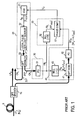
- Fig. 1 is a block diagram depicting an example of a conventional ultrahigh-speed clock extraction circuit described in European Patent Application Publication EP1119119A1 (corresponding US Patent Application Publication Gazette US2002/0027692A1).
- the illustrated ultrahigh-speed clock extraction circuit comprises: a local clock generating part 20 for generating a local clock CK L ; a local feedback signal generating 30 for generating a local feedback signal FB L ; an input signal component generating part 40 for extracting an input signal component SC R from an input optical signal pulse stream LP R ; and a phase comparison part 50 which compares the phases of the local feedback signal FB L and the input signal component SC R and provides the comparison result, as a voltage control signal V C , to the local clock generating part 20.
- the local clock generating part 20, the local feedback signal generating part 30 and the phase comparison part 50 constitute a phase-locked loop.
- the local clock generating part 20 is made up of a voltage-controlled oscillator 21, a local pulse generating light source 22, and an optical branching device 23.
- the input signal component generating part 40 is made up of an optical modulator 41, a photodetector 42 and a multiplexer 43.
- symbols in each pair of brackets [**] are intended to represent a frequency
- thick solid lines indicate optical signal paths and thin solid lines electrical signal paths.
- the input optical signal pulse stream LP R of a repetition frequency Nf a (where N is the number of multiplex channels), sent over an optical fiber transmission line 9, is branched by an optical branching device 11 into two, one of which is output as an original input optical signal pulse stream LP R and the other of which is fed to the optical modulator 41 of the input signal component generating part 40.
- the local pulse generating light source 22 is driven by a drive signal S D of a frequency f VCO from the voltage-controlled oscillator 21 to generate a local optical pulse stream LP L .
- the local optical pulse stream LP L is branched by the optical branching device 23 into two, one of which is output as the local clock CK L via a local output path 2LP and the other of which is fed via a feedback path 2FP to the photodetector 31 for conversion into the local feedback electrical signal FB L .
- the optical modulator 41 is one that has a property of linearly responding to the electrical drive signal, for example, an electroabsorption optical modulator.
- the input signal component SC R of a frequency Nf a -n(Lf VCO ) (where n is a natural number) is extracted by the photodetector 42 from the optical signal output from the optical modulator 41, and the extracted signal is provided to a phase comparator 51.
- the electrical feedback signal FB L branched from the photodetector 31 is M-multiplied by a multiplexer 52 into a signal FB L of a frequency Mf VCO , which is applied to the phase comparator 51 for comparison with the input signal component SC R of the frequency Nf a -n(Lf VCO ).
- An error signal resulting from the comparison is fed back as the voltage control signal V C to the voltage-controlled oscillator 21 to control its oscillation frequency f VCO .
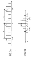
- Fig. 2A depicts the frequency spectrum of the output light from the optical modulator 41 when an optical pulse stream of a repetition frequency f 0 is modulated therein by the modulation signal S m of the frequency f m .
- the optical pulse stream of the repetition frequency f 0 has modulated components f c +f 0 and f c -f 0 on both sides of an optical carrier frequency f c .
- Modulating the optical pulse stream by the electrical signal S m of the frequency f m in the optical modulator 41 many modulated sidebands are newly generated by the frequency f m around the carrier component f c and the modulated components f c ⁇ f 0 , respectively, as shown in Fig. 2A.
- beat signals (f 0 ⁇ nf m , where n is a natural number) appear in its power spectrum at intervals f m about the repetition frequency f 0 as depicted in Fig. 2B. Even with the actual photodiode of limited frequency band, it is possible to detect beat signals in the low-frequency region.
- This case corresponds to the generation of an optical control pulse stream (i.e., local optical pulse stream LP L ) synchronized in bit phase with a time-division-multiplexed optical signal (i.e., input optical pulse stream LP R ) of a repetition frequency 160 GHz and having a repetition frequency 20 GHz.
- an optical control pulse stream i.e., local optical pulse stream LP L
- a time-division-multiplexed optical signal i.e., input optical pulse stream LP R
- the first and second beat components both contain exactly the same frequency 40 GHz.
- the first beat component of the frequency 160-nf m has the phase information of the input optical signal and is utilized in the phase-locked loop, but the second beat components kf m (frequencies 40, 80, ... GHz) do not contain the phase information of the input optical signal.
- the presence of the second beat components interferes with the phase comparison by the phase comparator 51 between the first beat component and the output component Mf VCO from the multiplexer 52, making the entire operation of the phase-locked loop unstable.
- f m 60 GHz; if the 40 GHz component is used as the first beat component (100, 40, ... (GHz)), it is possible to avoid the interference by the second beat component (60, 120, ... (GHz)) at the phase comparison frequency 40 GHz. In other words, it is possible to avoid that the first and second beat components contain the same frequency.
- f m 60 GHz (and 40 GHz as the phase comparison frequency) as the modulation frequency; in the present microwave technology, this scheme is appreciably disadvantageous in terms of cost and performance as compared with the case of using frequencies down to the K band lower than 26.5 GHz.
- any combinations of the parameters L, M and n neither permit cost reduction nor provide stability in the generation of the local clock CK L synchronized in bit phase with the 160 Gbit/s optical time-division-multiplexed signal and having the 20 GHz repetition frequency.
- the present invention offers a basic technique indispensable to stabilization of all-optical signal processing by compensating for delay fluctuations in the optical control signal generating system as well to thereby enable the received optical signal pulse stream and the optical control pulse stream to maintain their mutual positional relationship with errors between their bits held below subpicosecond.
- the ultrahigh-speed clock extraction circuit comprises:
- the ratio setting means it is possible to prevent that the frequency of the modulation signal for application to the optical modulator becomes a natural-number fraction of the repetition frequency Nf a of the input optical signal pulse stream. Accordingly, it is possible to avoid that the frequency of the down-converted electric signal having the phase information of the input optical signal becomes identical with the frequency that results from the modulation of he DC component of the input optical signal by the optical modulator.
- the local clock generating part may be formed by a voltage-controlled oscillator, a local pulse generating light source and an optical branching device, and the local feedback signal generating part may be formed by a photodetector and a frequency demultiplier.
- the local clock generating part may also be formed by a voltage-controlled oscillator and a multiplexer so that a local electrical clock is output as the local clock from the multiplier and the output from the voltage-controlled oscillator is applied as an electrical signal to the local feedback signal generating part to generate the local feedback signal.
- the local optical pulse from the local clock generating part may be applied to the local feedback signal generating part after being frequency demultiplied by an optical frequency demultiplier.
- the local clock may be multiplied by an optical multiplier to yield the output local clock. This permits suppression of the repetition frequency of the local optical pulse from the local optical pulse generating light source, by which it is possible to obtain in the phase-locked loop the same signal frequency as that obtainable by frequency demultiplying the photodetector output in the local feedback signal generating part.
- the ultrahigh-speed clock extraction circuit may also be adapted so that the local clock is multiplied by an optical multiplier to generate the output local clock while at the same time the feedback clock is frequency demultiplied in the local feedback signal generating part.
- Such individual generation of the two clocks increases flexibility in circuit design, providing increased operation stability and permitting cost reduction.
- the present invention provides a circuit for generating a local optical pulse stream or local electrical clock synchronized in phase with the input optical signal pulse stream.
- the circuit uses a phase detecting technique utilizing modulated sidebands resulting from optical modulation and a phase-locked loop technique.
- the phase comparison frequency in the phase-locked loop and the optical modulation frequency may sometimes become equal, making the operation of the phase-locked loop unstable.
- the present invention offers a construction having a frequency demultiplier in the phase-locked loop, a construction having an optical multiplier for K-multiplying the repetition frequency of the local optical pulse stream in the domain of light, and a construction provided with the frequency demultiplier and the optical multiplier in combination.
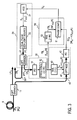
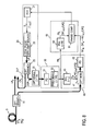
- Fig. 3 illustrates in block form a first embodiment of the ultrahigh-speed clock extraction circuit according to the present invention.
- the ultrahigh-speed clock extraction circuit of this embodiment is made up of the local clock generating part 20, the local feedback signal generating part 30, the input signal component generating part 40 and the phase comparison part 50; furthermore, the local clock generating part 20, the input signal component generating part 40 and the phase comparison part 50 are also identical in construction with the corresponding parts in Fig. 1.
- the local feedback signal generating part 30 includes a frequency demultiplier 32, which divides the frequency f VCO of the output signal from the photodetector 31 down to 1/K and outputs the local feedback signal FB L of the frequency f VCO /K.
- the input optical signal pulse stream LP R of the repetition frequency Nf a is branched by the optical branching device 11 into two, one of which is input to the optical modulator 41.
- the local pulse generating light source 22 is driven by the drive signal S D of the frequency f VCO from the voltage-controlled oscillator 21 to generate the local optical pulse stream LP L of the repetition frequency f VCO .
- the local optical pulse stream LP L is branched by the optical branching device 23 into two, one of which is provided via the feedback path 2FP to the photodetector 31 for conversion to an electrical signal.
- the optical modulator 41 used in this embodiment is a modulator which nonlinearly responds to the electrical drive signal (i.e. the modulation signal S m ), such as an intensity modulator, electroabsorption modulator, semiconductor optical modulator, optical comb generator, or optical phase modulator.
- the optical modulator 41 may also be formed by an optical modulator that has a linear response characteristic. The same is true of the embodiments described later on.
- the frequency demultiplier 32 is formed by, for example, a flip-flop circuit, pulse accumulation circuit, or feedback frequency demultiplier using a monostable multivibrator.
- a high-speed frequency demultiplier that operates at 20 GHz, there is available, for example, MOF08A(T-FF) by NTT Electronics, Ltd.
- the output optical signal from the optical modulator 41 is converted by the photodetector 42 to the input signal component electrical signal SC R of a frequency Nf a -(nL/K)f VCO (where n is a natural number), which is fed to the phase comparator 51.
- the other output signal from the frequency demultiplier 32 that is, the local feedback signal FB L , is M-multiplied by the multiplier 52, and the M-multiplied signal FB L is provided to the phase comparator 51 for phase comparison with the input signal component electrical signal SC R of the frequency Nf a -(nL/K)f VCO .
- An error signal resulting from the phase comparison is fed back as the voltage control signal V C to the voltage-controlled oscillator 21 to control its oscillation frequency f VCO .
- the local pulse stream LP L from the local pulse generating light source 22 is provided from the local output path 2LP as the local clock CK L which is in bit-phase synchronization with the input optical signal pulse stream LP R .
- the frequency demultiplier 32 in this embodiment constitutes ratio setting means for setting the frequency of the local feedback signal FB L to an integral (2 or larger) fraction of the frequency of the local output clock CK L .
- the multiplication numbers L and M of the multipliers 43 and 52 may take various values (natural numbers), depending on the degree of which of beat signals occurring in the optical modulator 41 is to be detected, or depending on the manner of selecting the frequency for phase comparison in the phase comparator 51.
- the frequency multiplication number is 1, the multiplier does not ever affect the input electrical signal, and hence it can be omitted. This applies to the following embodiments; that is, multipliers whose multiplication numbers are 1 can be omitted.
- the voltage-controlled oscillator 21 may be combined with a multiplier. That is, a voltage-controlled oscillator of a frequency (1/Q)f VCO and a multiplier of a multiplication number Q can be combined.
- the phase comparison frequency (Nf a -nf m ) may preferably be low so as to use commercially available digital PLL-IC (of a band ⁇ 1GHz) or the like. It must be noted here that the numerical values given in the rows Nos. 4 and 5 in Table 1 are examples intended to lower the phase comparison frequency Nf a -nf m .
- the configuration for decreasing the phase comparison frequency is already described as well in the afore-mentioned European Patent Application Publication EP1119119A1.
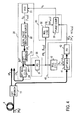
- Fig. 4 illustrates in block form a second embodiment of the ultrahigh-speed clock extraction circuit according to the present invention, which is a modified form of the first embodiment.
- the frequency demultiplier 32 is not provided in the local feedback signal generating part 30 as in the first embodiment, but instead an optical multiplier 24 is provided in the output path 2LP of the optical branching device 23 so that the output local clock is J-multiplied.
- the frequency of the local feedback signal FB L which is output from the feedback signal generating part 30 is f VCO
- the frequency of the input signal component SC R for application from the photodetector 42 to the phase comparator 51 is Nf a -nLf VCO
- the frequency of the signal for application from the multiplier 52 to the phase comparator 51 is Mf VCO ; the values of the integers L and M are chosen so that these two frequencies become equal to each other. No description will be repeated on the other parts and operations since they are similar to those in Embodiment 1.
- the local pulse stream LP L from the local pulse generating light source 22, which is output from the optical branching device 23, is in bit-phase synchronization with the input optical signal pulse stream LP R .
- the repetition frequency f VCO of the local optical pulse stream LP L is J-multiplied by the optical multiplier 24 to provide the local clock CK L of a frequency Jf VCO .
- the optical multiplier 24 in this embodiment constitutes ratio setting means for setting the frequency of the local feedback signal FB L to an integral (2 or larger) multiple of the local clock CK L .
- Fig. 5A illustrates in block form an example of the optical multiplier 24.
- the optical splitter 24A and the optical combiner 24B can each be formed by a multi-mode interference coupler such as a fusion-elongated optical fiber coupler or planar lightwave device.
- Fig. 4B illustrates another example of the optical multiplier 24.
- multipliers of a multiplication number 1 can be omitted. Since the multiplication number M in both rows Nos. 1 and 2 in Table 2 is 1, the multiplier 52 concerned can be omitted.
- the speedup of the local pulse generating light source 22 increases the workload of a high-frequency circuit for driving it, and further, the attainment of the required optical SN ratio calls for larger mean optical power ⁇ this increases the workload on the light source itself and an optical amplifier (the light source is usually formed by a combination of a laser light emitting element and an optical fiber amplifier). Accordingly, the suppression of the oscillation frequency of the light source 22 improves the operation stability of the entire system and reduces its cost.
- Fig. 6 illustrates in block form a third embodiment of the ultrahigh-speed clock extraction circuit according to the present invention, which is a another modified form of the first embodiment.
- this embodiment uses the optical multiplier 24 added to the output path 2LP of the optical branching device 23 in the first embodiment of Fig. 3.
- the operation of this embodiment is the same as described above with reference to the first and second embodiments.
- the optical multiplier 24 and the frequency demultiplier 32 constitute ratio setting means for setting the frequency of the local feedback signal FB L to an integral (2 or larger) fraction of the frequency of the local clock CK L .
- Table 3 shows examples of concrete numerical values in his embodiment. Concrete numerical values in Embodiment 3 No. Nf f N f a f VCO J K L M f m n Nf a -nf m 1 160Gbit/s 4 40GHz 20GHz 2 2 3 1 30GHz 5 10GHz 2 320Gbit/s 8 40GHz 20GHz 2 2 3 2 30GHz 10 20GHz 3 160Gbit/s 4 40GHz 20GHz 2 8 3 1 7.5GHz 21 2.5GHz 4 320Gbit/s 8 40GHz 20GHz 2 8 3 2 7.5GHz 42 5GHz
- This embodiment differs from the first and second embodiments in that 20 GHz can be selected as the frequency f VCO of the voltage-controlled oscillator 21 in the case of generating the 20 GHz local clock stream CK L .
- a mode-locked semiconductor laser is used as the light source 22 since the repetition frequency and the resonator length are in inverse proportion to each other, a decrease in the repetition frequency causes an increase in the resonator length, making the fabrication of the laser more difficult.
- a 10 GHz repetition frequency allows more ease in the fabrication of mode-locked semiconductor laser than a 20 GHz repetition frequency.
- the configuration using the 20 GHz light source becomes possible for the first time with this embodiment.
- the speedup of the light source 22 usually increases the workload for the other parts, but in some cases a low-speed operation is not optimum from the viewpoint of its fabrication as described above.
- This embodiment is intended to solve such a problem and is advantageous in that the combined use of the electrical frequency demultiplier 32 and the optical multiplier 24 enables implementation of more flexible phase-locked loop circuitry, providing increased operation stability and permitting cost reduction.
- Fig. 7 illustrates in block form a fourth embodiment of the ultrahigh-speed clock extraction circuit according to the present invention. Unlike the first to third embodiments this embodiment outputs an electrical locally generated clock CK L synchronized with the input optical signal pulse stream LP R instead of outputting the optical clock. More specifically, the light source 22 and the photodetector 31 in the third embodiment of Fig. 6 are removed, and the optical branching device 23 and the optical multiplier 24 are replaced with an electrical branching device 23' and an electrical multiplier 24'. The output from the voltage-controlled oscillator 21 is branched by the branching device 23' to the multiplier 24' and the frequency demultiplier 32.
- the output signal of the frequency f VCO from the voltage-controlled oscillator 21 is J-multiplied by the multiplier 24', and the phase-locked loop is configured so that the electrical local clock CK L fed from the multiplier 24' coincides with the phase of the input optical signal pulse stream LP R .
- the multiplier 24' corresponds to the optical multiplier 24 in the second embodiment, by which an increase in the frequency in the phase-locked loop can be suppressed. Further, the combined use of the frequency demultiplier 32 and the multiplier 24' corresponds to the combined use of the frequency demultiplier 32 and the optical multiplier 24 in the third embodiment. When the frequency demultiplication number K is 1, the frequency demultiplier 32 can be omitted.
- the multiplier 24' and the frequency demultiplier 32 constitute ratio setting means for setting the frequency of the local feedback signal FB L to an integral (2 or larger) fraction of the frequency of the local output clock CK L .
- Table 4 shows examples of concrete numerical values of the parameters in the fourth embodiment. Examples of concrete numerical values in Embodiment 4 No. Nf a N f a f VCO J K L M f m n Nf a -nf m 1 160Gbit/s 8 20GHz 10GHz 2 1 3 1 30GHz 5 10GHz 2 160Gbit/s 4 40GHz 20GHz 2 2 3 1 30GHz 5 10GHz 3 320Gbit/s 8 40GHz 20GHz 2 2 3 2 30GHz 10 20GHz 4 160Gbit/s 8 20GHz 10GHz 2 4 3 1 7.5GHz 21 2.5GHz 5 160Gbit/s 4 40GHz 20GHz 2 8 3 1 7.5GHz 21 2.5GHz 6 320Gbit/s 8 40GHz 20GHz 2 8 3 2 7.5GHz 42 5GHz
- the output local electrical clock C in this embodiment is phase-synchronized with the input optical signal pulse stream A; therefore, by using this clock as a drive signal for the electroabsoprtion optical modulator that is, for example, an electrical-control-type optical gate, it can be operated as an optical time-division demultiplexer for the input optical signal.
- Fig. 8 illustrates in block form a fifth embodiment of the ultrahigh-speed clock extraction circuit, which is a modification of the third embodiment shown in Fig. 6.
- the optical multiplier 24 inserted in the output path 2LP in the third embodiment is replaced with an optical demultiplier 25 inserted in the feedback path 2FP, by which the local feedback clock CK L of the frequency f VCO is frequency divided down to 1/J and the output of which is applied to the photodetector 31.
- the optical demultiplier 25 and the frequency demultiplier 32 constitute ratio setting means for setting the frequency of the locally generated feedback signal FB L to an integral (2 or larger) fraction of the frequency of the locally generated output clock CK L .
- this embodiment provides greater flexibility in the design of the phase-locked loop, providing increased operation stability and permitting cost reduction.
- Table 5 shows concrete examples of numerical values in this embodiment. Concrete example of numerical values in Embodiment 5 No. Nf a N f a f VCO J K L M f m n Nf a -nf m 1 160Gbit/s 4 40GHz 40GHz 2 2 3 1 30GHz 5 10GHz 2 320Gbit/s 8 40GHz 40GHz 2 2 3 2 30GHz 10 20GHz 3 160Gbit/s 4 40GHz 40GHz 4 1 3 1 30GHz 5 10GHz 4 320Gbit/s 8 40GHz 40GHz 4 1 3 2 30GHz 10 20GHz 5 160Gbit/s 4 40GHz 40GHz 4 4 3 1 7.5GHz 21 2.5GHz 6 160Gbit/s 4 40GHz 40GHz 2 8 3 1 7.5GHz 21 2.5GHz 7 320Gbit/s 8 40GHz 40GHz 4 4 3 2 7.5GHz 42 5GHz 8 320Gbit/s 8 40GHz 40GHz 40GHz 2 8 3 2 7.5GHz 42 5GHz
- Fig. 9 depicts in block form a concrete example of the optical demultiplier 25.
- the optical demultiplier 25 possesses the function of frequency-dividing down to 1/J the repetition of the local optical pulse stream of the repetition frequency f VCO input thereto via the feedback path 2FP from the optical branching device 23 and applying the frequency-divided output to the feedback local signal generating part 30.
- Fig. 9 depicts in block form a concrete example of the optical demultiplier 25.
- the optical demultiplier 25 possesses the function of frequency-dividing down to 1/J the repetition of the local optical pulse stream of the repetition frequency f VCO input thereto via the feedback path 2FP from the optical branching device 23 and applying the frequency-divided output to the feedback local signal generating part 30.
- the optical demultiplier 25 comprises an intensity modulator 25A and a frequency demultiplier 25B, and frequency-divides the drive signal of the frequency f VCO from the voltage-controlled oscillator 21 down to 1/J to generate an electrical signal of a frequency (1/J)f VCO , which is applied to the intensity modulator 25A to gate the local feedback clock CK L with a period J/f VCO , thereby extracting optical pulses.
- the repetition frequency of the local feedback clock CK L can be demultiplied down to f VCO /J.
- the voltage-controlled oscillator 21 can be implemented by a combination of a voltage-controlled oscillator of a frequency lower than f VCO and a multiplier as described previously with reference to the first embodiment, the use of an appropriate multiplier will permit generation of an electrical signal of the frequency (1/J)f VCO .
- the frequency demultiplier 25B is unnecessary since the output of the frequency f VCO /J from the voltage-controlled oscillator needs only to be applied directly to the intensity modulator 25.
- the intensity modulator can be formed using, for example, an LiNbO 3 Mach-Zehnder optical modulator or electroabsorption optical modulator.
- the gate width of such an intensity modulator is as large as several tens of picosecond; for example, when it is driven by a 10 GHz sine wave, the intensity modulator accommodates a phase shift between the drive electrical signal and the local optical pulse stream which is caused by a fluctuation delay occurring in the local optical pulse stream generating part. Hence, the frequency demultiplying operation does not become unstable.
- Fig. 10 depicts another concrete example of the optical demultiplier 25.
- This example is common to the Fig. 9 example in the implementation of optical demultiplication by thinning out local optical pulse stream through use of the intensity modulator 25A, but differs from the latter in the way of generating an electrical signal for driving the intensity modulator 25A.
- the local feedback clock CK L is branched by an optical coupler 25C from the feedback path 2FP and the branched output is fed to a clock regenerator 25D, which extracts an electrical clock of the frequency f VCO /J which is a J-demultiplied version of the local feedback clock CK L of the frequency f VCO and from which the extracted electrical clock is provided to the intensity modulator 25A.
- the ultrahigh-speed clock extraction circuit precludes the possibility that in the case of a particular combination of the repetition frequency of the input optical signal pulse stream and the repetition frequency of a local optical pulse stream or the frequency of a local electrical clock, the frequency of a modulation signal of the optical modulator and a frequency of its natural-number multiple become equal to a frequency down-converted from the input optical signal pulse stream, thereby solving the problem of unstable operation of the clock extraction circuit.
- the particular combination of frequencies refers to the case where the repetition frequencies of, for example, the input optical signal pulse stream and the local optical pulse stream are 160 Gbit/s and 20 GHz, respectively.
- the 160 Gbit/s frequency will be very likely used as a standard repetition frequency of the optical time-division-multiplexed signal, and hence it is very important.
Landscapes
- Physics & Mathematics (AREA)
- Optics & Photonics (AREA)
- Engineering & Computer Science (AREA)
- Computer Networks & Wireless Communication (AREA)
- Signal Processing (AREA)
- Optical Communication System (AREA)
- Optical Modulation, Optical Deflection, Nonlinear Optics, Optical Demodulation, Optical Logic Elements (AREA)
- Synchronisation In Digital Transmission Systems (AREA)
- Stabilization Of Oscillater, Synchronisation, Frequency Synthesizers (AREA)
Abstract
Description
| Concrete examples of numerical values in | ||||||||||
| No. | Nfa | N | fa | fVCO | K | L | M | fm | n | Nfa- |
| 1 | 160Gbit/s | 8 | 20GHz | 20GHz | 2 | 3 | 1 | 30GHz | 5 | |
| 2 | 160Gbit/s | 4 | 40GHz | 40GHz | 4 | 3 | 1 | 30GHz | 5 | 106Hz |
| 3 | 320Gbit/s | 8 | 40GHz | 40GHz | 4 | 3 | 2 | 30GHz | 10 | 20GHz |
| 4 | 160GHz | 8 | 20GHz | 20GHz | 8 | 3 | 1 | 7.5 | 21 | 2.5GHz |
| 5 | 160GHz | 4 | 40GHz | 40GHz | 16 | 3 | 1 | 7.5 | 21 | 2.5GHz |
| Concrete examples of numerical values in | ||||||||||
| No. | Nfa | N | fa | fVCO | J | L | M | fm | N | Nfa- |
| 1 | 160Gbit/s | 8 | 20GHz | 10GHz | 2 | 3 | 1 | 30GHz | 5 | |
| 2 | 160Gbit/s | 4 | 40GHz | 10GHz | 4 | 3 | 1 | 30GHz | 5 | 10GHz |
| 3 | 320Gbit/s | 8 | 40GHz | 10GHz | 4 | 3 | 2 | 30GHz | 10 | 20GHz |
| Concrete numerical values in Embodiment 3 | |||||||||||
| No. | Nff | N | fa | fVCO | J | K | L | M | fm | n | Nfa- |
| 1 | 160Gbit/s | 4 | 40GHz | 20GHz | 2 | 2 | 3 | 1 | 30GHz | 5 | |
| 2 | 320Gbit/s | 8 | 40GHz | 20GHz | 2 | 2 | 3 | 2 | 30GHz | 10 | 20GHz |
| 3 | 160Gbit/s | 4 | 40GHz | 20GHz | 2 | 8 | 3 | 1 | 7.5 | 21 | 2.5GHz |
| 4 | 320Gbit/s | 8 | 40GHz | 20GHz | 2 | 8 | 3 | 2 | 7.5 | 42 | 5GHz |
| Examples of concrete numerical values in Embodiment 4 | |||||||||||
| No. | Nfa | N | fa | fVCO | J | K | L | M | fm | n | Nfa- |
| 1 | 160Gbit/s | 8 | 20GHz | 10GHz | 2 | 1 | 3 | 1 | 30GHz | 5 | |
| 2 | 160Gbit/s | 4 | 40GHz | 20GHz | 2 | 2 | 3 | 1 | 30GHz | 5 | 10GHz |
| 3 | 320Gbit/s | 8 | 40GHz | 20GHz | 2 | 2 | 3 | 2 | 30GHz | 10 | 20GHz |
| 4 | 160Gbit/s | 8 | 20GHz | 10GHz | 2 | 4 | 3 | 1 | 7.5 | 21 | 2.5GHz |
| 5 | 160Gbit/s | 4 | 40GHz | 20GHz | 2 | 8 | 3 | 1 | 7.5 | 21 | 2.5GHz |
| 6 | 320Gbit/s | 8 | 40GHz | 20GHz | 2 | 8 | 3 | 2 | 7.5 | 42 | 5GHz |
| Concrete example of numerical values in Embodiment 5 | |||||||||||
| No. | Nfa | N | fa | fVCO | J | K | L | M | fm | n | Nfa- |
| 1 | 160Gbit/s | 4 | 40GHz | 40GHz | 2 | 2 | 3 | 1 | 30GHz | 5 | |
| 2 | 320Gbit/s | 8 | 40GHz | 40GHz | 2 | 2 | 3 | 2 | 30GHz | 10 | 20GHz |
| 3 | 160Gbit/s | 4 | 40GHz | 40GHz | 4 | 1 | 3 | 1 | 30GHz | 5 | 10GHz |
| 4 | 320Gbit/s | 8 | 40GHz | 40GHz | 4 | 1 | 3 | 2 | 30GHz | 10 | 20GHz |
| 5 | 160Gbit/s | 4 | 40GHz | 40GHz | 4 | 4 | 3 | 1 | 7.5 | 21 | 2.5GHz |
| 6 | 160Gbit/s | 4 | 40GHz | 40GHz | 2 | 8 | 3 | 1 | 7.5 | 21 | 2.5GHz |
| 7 | 320Gbit/s | 8 | 40GHz | 40GHz | 4 | 4 | 3 | 2 | 7.5 | 42 | 5GHz |
| 8 | 320Gbit/s | 8 | 40GHz | 40GHz | 2 | 8 | 3 | 2 | 7.5 | 42 | 5GHz |
Claims (13)
- An ultrahigh-speed clock extraction circuit for obtaining a local clock synchronized in bit phase with an input optical signal pulse stream, said extraction circuit comprising:wherein a path containing said phase comparison part, said local clock generating part and said local feedback signal generating part constitutes a phase-locked loop for said input signal component electrical signal.a local clock generating part which generates a local clock of a frequency controlled by a voltage control signal and branches the local clock into a local output clock and a local feedback clock;a local feedback signal generating part which generates a local feedback signal from said local feedback clock;an input signal component generating part made up of a modulation signal generating part for generating a modulation signal containing phase information of said local feedback signal, an optical modulator for modulating an input optical signal pulse stream by said modulation signal to generate a modulated input optical signal stream, and a photodetector supplied with said modulated input optical signal pulse stream, for outputting an input signal component electrical signal having a down-converted frequency of said modulated input optical signal pulse stream and having bit-phase information thereof;a phase comparison part which compares the phases of said local feedback signal and said input signal component electrical signal and outputs, as said voltage control signal, the voltage corresponding to their phase difference; andratio setting means which sets the frequency of said local feedback signal to an integral fraction of the frequency of said output local clock so that said down-converted frequency of said input signal component electrical signal differs from a natural-number multiple of the frequency of said modulation signal;
- The circuit of claim 1, wherein said local clock generating part comprises a voltage-controlled oscillator for generating a drive signal of a frequency controlled by said voltage control signal, a local pulse generating light source driven by said drive signal to generate a local optical pulse stream, and an optical branching device for branching said local optical pulse stream into said output local clock and said local feedback clock; and
wherein said local feedback signal generating part comprises a photodetector for converting said local feedback clock to a local electrical signal, and a frequency demultiplier for frequency-demultiplying said local electrical signal down to 1/K to generate said local feedback signal, said K being an integer equal to or greater than 1 and said frequency demultiplier forming said ratio setting means. - The circuit of claim 1, wherein said local clock generating part comprises a voltage-controlled oscillator for generating a local clock of a frequency controlled by said voltage control signal, and a J multiplier for J-multiplying one of two branched versions of said local clock from said voltage-controlled oscillator to provide an output local clock, said J being an integer equal to or greater than 2;
wherein said local feedback signal generating part includes a 1/K frequency demuliplier for frequency-demultiplying the other branched version of said local clock down to 1/K to provide said local feedback signal, said K being an integer equal to or greater than 1; and
wherein said J multiplier and said 1/L frequency demultiplier constitute said ratio setting means. - The circuit of claim 1, wherein said local clock generating part comprises a voltage-controlled oscillator for generating a drive signal of a frequency controlled by said voltage control signal, a local pulse generating light source driven by said drive signal to generate local optical pulse stream, an optical branching device for branching said local optical pulse stream into two outputs, one of said two branched outputs being provided as said output local clock, and an optical frequency demultiplier for frequency demultiplying the other of said two branched outputs down to 1/J to generate said local feedback clock, said J being an integer equal to or greater than 2;
wherein said local feedback signal generating part comprises a photodetector for converting said local feedback clock to a local electrical signal, and a frequency demultiplier for frequency demultiplying said local electrical signal down to 1/K to generate said local feedback signal, said K being an integer equal to or greater than 1; and
wherein said optical frequency demultiplier and said frequency demultiplier constitute said ratio setting means. - The circuit of claim 1, wherein said local clock generating part comprises a voltage-controlled oscillator for generating a drive signal of a frequency controlled by said voltage control signal, a local pulse generating light source driven by said drive signal to generate a local optical pulse stream, an optical branching device for branching said local optical pulse stream into two outputs, one of said two branched output being provided as said local feedback clock, and an optical multiplier for J-multiplying the other of said two branched output to generate said output local clock, said J being an integer equal to or greater than 2 and said optical multiplier forming said ratio setting means; and
wherein said local feedback signal generating part includes a photodetector for converting said local feedback optical pulse stream to a local feedback signal. - The circuit of claim 1, wherein said local clock generating part comprises a voltage-controlled oscillator for generating a drive signal of a frequency controlled by said voltage control signal, a local pulse generating light source driven by said drive signal to generate a local optical pulse stream, an optical branching device for branching said local optical pulse stream into two outputs, one of said two branched output being provided as said local feedback clock, and an optical multiplier for J-multiplying the other of said two branched output to generate said output local clock, said J being an integer equal to or greater than 2 and said optical multiplier forming said ratio setting means; and
wherein said local feedback signal generating part comprises photodetector for converting said local feedback clock into a local electrical signal, and a 1/K frequency demultiplier for frequency demultiplying said local electrical signal down to 1/K to generate said local feedback signal, said K being an integer equal to or greater than 2 and said optical multiplier and said 1/K frequency demultiplier constituting said ratio setting means. - The circuit of any one of claims 1 to 6, wherein said optical modulator is an intensity modulator.
- The circuit of any one of claims 1 to 6, wherein said optical modulator is an electroabsorption optical modulator.
- The circuit of any one of claims 1 to 6, wherein said optical modulator is an optical comb generator.
- The circuit of any one of claims 1 to 6, wherein said optical modulator is an optical phase modulator.
- The circuit of any one of claims 1 to 6, wherein said optical modulator is a semiconductor optical amplifier.
- The circuit of any one of claims 1 to 6, wherein said phase comparison part comprises a multiplier for M-multiplying said local feedback signal from said local feedback signal generating part, said M being an integer equal to or greater than 1, and a phase comparator for detecting a phase difference between the output from said multiplier and said input signal component electrical signal from said input signal component generating part and for outputting said detected phase difference as said voltage control signal.
- The circuit of any one of claims 1 to 6, wherein said modulation signal generating part is a multiplier for L-multiplying said local negative feedback signal to generate said modulation signal, said L being an integer equal to or greater than 1.
Applications Claiming Priority (2)
| Application Number | Priority Date | Filing Date | Title |
|---|---|---|---|
| JP2001337636A JP3743626B2 (en) | 2001-11-02 | 2001-11-02 | Ultra-high-speed clock extraction circuit |
| JP2001337636 | 2001-11-02 |
Publications (3)
| Publication Number | Publication Date |
|---|---|
| EP1309123A2 true EP1309123A2 (en) | 2003-05-07 |
| EP1309123A3 EP1309123A3 (en) | 2004-06-23 |
| EP1309123B1 EP1309123B1 (en) | 2005-12-21 |
Family
ID=19152237
Family Applications (1)
| Application Number | Title | Priority Date | Filing Date |
|---|---|---|---|
| EP02024538A Expired - Lifetime EP1309123B1 (en) | 2001-11-02 | 2002-10-31 | Ultrahigh-speed clock extraction circuit for optical signals |
Country Status (4)
| Country | Link |
|---|---|
| US (1) | US7024122B2 (en) |
| EP (1) | EP1309123B1 (en) |
| JP (1) | JP3743626B2 (en) |
| DE (1) | DE60208145T2 (en) |
Families Citing this family (7)
| Publication number | Priority date | Publication date | Assignee | Title |
|---|---|---|---|---|
| DE10340030A1 (en) * | 2003-08-28 | 2005-04-07 | Siemens Ag | Clock regenerator for high data rate optical signal has frequency multiplier that produces modulation signal from clock signal with multiple of clock signal frequency and its fundamental frequency |
| US7593644B2 (en) * | 2004-05-12 | 2009-09-22 | Massachusetts Institute Of Technology | Synchronization of lasers and RF sources using timing information transfer in the optical domain |
| WO2006120281A1 (en) * | 2005-05-12 | 2006-11-16 | Perlos Oyj | Optical signal processing device |
| JP4725843B2 (en) * | 2005-08-25 | 2011-07-13 | 横河電機株式会社 | Optical packet network system |
| US7403054B1 (en) | 2007-12-05 | 2008-07-22 | International Business Machines Corporation | Sub-picosecond multiphase clock generator |
| JP5888635B2 (en) * | 2010-08-05 | 2016-03-22 | 国立大学法人東北大学 | Coherent optical time division multiplexing transmission equipment |
| FR3076959B1 (en) * | 2018-01-12 | 2020-07-17 | Amplitude Systemes | LASER SYSTEM AND METHOD FOR GENERATING VERY HIGH THROUGHPUT LASER PULSES |
Family Cites Families (5)
| Publication number | Priority date | Publication date | Assignee | Title |
|---|---|---|---|---|
| EP0595206A3 (en) * | 1992-10-30 | 1995-01-11 | Siemens Ag | Optical pulse synchronization device. |
| US5574588A (en) * | 1994-02-23 | 1996-11-12 | Nippon Telegraph And Telephone Corporation | Phase lock loop circuit using optical correlation detection |
| CN1175334A (en) * | 1994-12-23 | 1998-03-04 | 英国电讯公司 | Nodes in Optical Time Division Multiplexing Networks |
| JP3296994B2 (en) * | 1996-11-21 | 2002-07-02 | 日本電信電話株式会社 | Ultra-high-speed clock extraction circuit |
| JP3549801B2 (en) * | 2000-01-20 | 2004-08-04 | 日本電信電話株式会社 | Bit phase synchronization local oscillator pulse train generation circuit |
-
2001
- 2001-11-02 JP JP2001337636A patent/JP3743626B2/en not_active Expired - Fee Related
-
2002
- 2002-10-31 EP EP02024538A patent/EP1309123B1/en not_active Expired - Lifetime
- 2002-10-31 DE DE60208145T patent/DE60208145T2/en not_active Expired - Lifetime
- 2002-11-01 US US10/285,525 patent/US7024122B2/en not_active Expired - Fee Related
Also Published As
| Publication number | Publication date |
|---|---|
| EP1309123B1 (en) | 2005-12-21 |
| US7024122B2 (en) | 2006-04-04 |
| JP3743626B2 (en) | 2006-02-08 |
| DE60208145D1 (en) | 2006-01-26 |
| DE60208145T2 (en) | 2006-07-20 |
| JP2003143073A (en) | 2003-05-16 |
| US20030117196A1 (en) | 2003-06-26 |
| EP1309123A3 (en) | 2004-06-23 |
Similar Documents
| Publication | Publication Date | Title |
|---|---|---|
| Devgan | A review of optoelectronic oscillators for high speed signal processing applications | |
| US5652669A (en) | Optical synchronization arrangement | |
| Boerner et al. | 160 Gbit/s clock recovery with electro-optical PLL using a bidirectionally operated electroabsorption modulator as phase comparator | |
| EP1895689B1 (en) | Wavelength variable laser | |
| US7058312B2 (en) | Opto-electronic phase-locked loop with microwave mixing for clock recovery | |
| EP1119119B1 (en) | Local generator with PLL for phase synchronization of clock signal with bits in optical pulse stream | |
| EP1318627B1 (en) | Optical clock phase-locked loop circuit | |
| US20050190432A1 (en) | Optical device for optical communication | |
| EP1309123B1 (en) | Ultrahigh-speed clock extraction circuit for optical signals | |
| US7623792B2 (en) | Clock extracting method and apparatus thereof | |
| Tong et al. | Optoelectronic phase-locked loop with balanced photodetection for clock recovery in high-speed optical time-division-multiplexed systems | |
| JP3447664B2 (en) | Optical transmitter and optical transmitter control method | |
| Chou et al. | High-speed OTDM and WDM networks using traveling-wave electroabsorption modulators | |
| Hu et al. | Optical clock recovery circuits using traveling-wave electroabsorption modulator-based ring oscillators for 3R regeneration | |
| AU727247B2 (en) | Channel selection in an optical TDMA network | |
| US7197249B2 (en) | Method and system for synchronizing optical clocks | |
| US7035542B2 (en) | All-optical high bit-rate multiplexer | |
| JPH04163532A (en) | Light clock extraction circuit | |
| WO1993016514A1 (en) | Frequency changing of light signals | |
| Dennis et al. | Eight-to-one demultiplexing of 100-Gbit/s TDM data using LiNbO/sub 3/Sagnac interferometer modulators | |
| US20260046031A1 (en) | A clock signal distribution circuit | |
| JP2001094199A (en) | Optical clock sampling circuit and optical communication system | |
| JP3449019B2 (en) | Optical multiplexing equipment | |
| Yao et al. | Novel photonic clock and carrier recovery device | |
| Bogoni et al. | Electrical equivalent model for an optical VCO in a PLL synchronization scheme for ultrashort optical pulse sources |
Legal Events
| Date | Code | Title | Description |
|---|---|---|---|
| PUAI | Public reference made under article 153(3) epc to a published international application that has entered the european phase |
Free format text: ORIGINAL CODE: 0009012 |
|
| 17P | Request for examination filed |
Effective date: 20021031 |
|
| AK | Designated contracting states |
Designated state(s): AT BE BG CH CY CZ DE DK EE ES FI FR GB GR IE IT LI LU MC NL PT SE SK TR |
|
| AX | Request for extension of the european patent |
Extension state: AL LT LV MK RO SI |
|
| PUAL | Search report despatched |
Free format text: ORIGINAL CODE: 0009013 |
|
| AK | Designated contracting states |
Kind code of ref document: A3 Designated state(s): AT BE BG CH CY CZ DE DK EE ES FI FR GB GR IE IT LI LU MC NL PT SE SK TR |
|
| AX | Request for extension of the european patent |
Extension state: AL LT LV MK RO SI |
|
| RIC1 | Information provided on ipc code assigned before grant |
Ipc: 7H 04L 7/00 A Ipc: 7H 03L 7/18 B Ipc: 7H 03L 7/08 B Ipc: 7H 04J 14/08 B Ipc: 7H 03L 7/20 B |
|
| 17Q | First examination report despatched |
Effective date: 20050124 |
|
| AKX | Designation fees paid |
Designated state(s): DE FR GB |
|
| GRAP | Despatch of communication of intention to grant a patent |
Free format text: ORIGINAL CODE: EPIDOSNIGR1 |
|
| RIC1 | Information provided on ipc code assigned before grant |
Ipc: 7H 03L 7/18 B Ipc: 7H 04L 7/00 A Ipc: 7H 03L 7/08 B |
|
| GRAS | Grant fee paid |
Free format text: ORIGINAL CODE: EPIDOSNIGR3 |
|
| GRAA | (expected) grant |
Free format text: ORIGINAL CODE: 0009210 |
|
| AK | Designated contracting states |
Kind code of ref document: B1 Designated state(s): DE FR GB |
|
| REG | Reference to a national code |
Ref country code: GB Ref legal event code: FG4D |
|
| REF | Corresponds to: |
Ref document number: 60208145 Country of ref document: DE Date of ref document: 20060126 Kind code of ref document: P |
|
| ET | Fr: translation filed | ||
| PLBE | No opposition filed within time limit |
Free format text: ORIGINAL CODE: 0009261 |
|
| STAA | Information on the status of an ep patent application or granted ep patent |
Free format text: STATUS: NO OPPOSITION FILED WITHIN TIME LIMIT |
|
| 26N | No opposition filed |
Effective date: 20060922 |
|
| PGFP | Annual fee paid to national office [announced via postgrant information from national office to epo] |
Ref country code: FR Payment date: 20100908 Year of fee payment: 9 |
|
| PGFP | Annual fee paid to national office [announced via postgrant information from national office to epo] |
Ref country code: DE Payment date: 20101029 Year of fee payment: 9 |
|
| PGFP | Annual fee paid to national office [announced via postgrant information from national office to epo] |
Ref country code: GB Payment date: 20101027 Year of fee payment: 9 |
|
| GBPC | Gb: european patent ceased through non-payment of renewal fee |
Effective date: 20111031 |
|
| REG | Reference to a national code |
Ref country code: FR Ref legal event code: ST Effective date: 20120629 |
|
| PG25 | Lapsed in a contracting state [announced via postgrant information from national office to epo] |
Ref country code: DE Free format text: LAPSE BECAUSE OF NON-PAYMENT OF DUE FEES Effective date: 20120501 |
|
| REG | Reference to a national code |
Ref country code: DE Ref legal event code: R119 Ref document number: 60208145 Country of ref document: DE Effective date: 20120501 |
|
| PG25 | Lapsed in a contracting state [announced via postgrant information from national office to epo] |
Ref country code: GB Free format text: LAPSE BECAUSE OF NON-PAYMENT OF DUE FEES Effective date: 20111031 Ref country code: FR Free format text: LAPSE BECAUSE OF NON-PAYMENT OF DUE FEES Effective date: 20111102 |