EP1309114A2 - Equalization of optical signals - Google Patents
Equalization of optical signals Download PDFInfo
- Publication number
- EP1309114A2 EP1309114A2 EP02020312A EP02020312A EP1309114A2 EP 1309114 A2 EP1309114 A2 EP 1309114A2 EP 02020312 A EP02020312 A EP 02020312A EP 02020312 A EP02020312 A EP 02020312A EP 1309114 A2 EP1309114 A2 EP 1309114A2
- Authority
- EP
- European Patent Office
- Prior art keywords
- beams
- optical
- signal
- optically
- components
- Prior art date
- Legal status (The legal status is an assumption and is not a legal conclusion. Google has not performed a legal analysis and makes no representation as to the accuracy of the status listed.)
- Granted
Links
- 230000003287 optical effect Effects 0.000 title claims abstract description 131
- 238000000034 method Methods 0.000 claims abstract description 21
- 238000004891 communication Methods 0.000 description 19
- 230000010287 polarization Effects 0.000 description 14
- 230000003111 delayed effect Effects 0.000 description 13
- 238000010586 diagram Methods 0.000 description 10
- 230000004044 response Effects 0.000 description 8
- 230000001934 delay Effects 0.000 description 7
- 239000013078 crystal Substances 0.000 description 5
- 230000000644 propagated effect Effects 0.000 description 5
- 230000006735 deficit Effects 0.000 description 4
- 238000012986 modification Methods 0.000 description 3
- 230000004048 modification Effects 0.000 description 3
- 239000013307 optical fiber Substances 0.000 description 3
- 230000003044 adaptive effect Effects 0.000 description 2
- 210000002858 crystal cell Anatomy 0.000 description 2
- 238000001514 detection method Methods 0.000 description 2
- 238000005516 engineering process Methods 0.000 description 2
- 239000004973 liquid crystal related substance Substances 0.000 description 2
- 239000000463 material Substances 0.000 description 2
- 230000001902 propagating effect Effects 0.000 description 2
- 238000013459 approach Methods 0.000 description 1
- 230000005540 biological transmission Effects 0.000 description 1
- 230000015572 biosynthetic process Effects 0.000 description 1
- 210000004027 cell Anatomy 0.000 description 1
- 230000008859 change Effects 0.000 description 1
- 238000012937 correction Methods 0.000 description 1
- 230000007423 decrease Effects 0.000 description 1
- 230000000704 physical effect Effects 0.000 description 1
- 229920003023 plastic Polymers 0.000 description 1
- 230000035945 sensitivity Effects 0.000 description 1
- 239000012780 transparent material Substances 0.000 description 1
Images



Classifications
-
- H—ELECTRICITY
- H04—ELECTRIC COMMUNICATION TECHNIQUE
- H04B—TRANSMISSION
- H04B10/00—Transmission systems employing electromagnetic waves other than radio-waves, e.g. infrared, visible or ultraviolet light, or employing corpuscular radiation, e.g. quantum communication
- H04B10/25—Arrangements specific to fibre transmission
- H04B10/2507—Arrangements specific to fibre transmission for the reduction or elimination of distortion or dispersion
Definitions
- the present invention generally relates to communications. More specifically, the invention relates to equalization of signals propagated via communications systems.
- Optical communication systems tend to offer greater capacity or "bandwidth" than entirely electrically-based communication systems.
- even current optical communication systems typically use electrical signals and light pulses to communicate information.
- transmit components of such an optical communication system convert electrical signals into light pulses. These light pulses are propagated via an optical circuit that defines one or more optical paths.
- Receive components communicating with the optical paths convert the light pulses back to electrical signals.
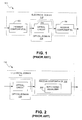
- Optical communication system 100 generally includes an electrical domain 102 and an optical domain 104.
- Electrical domain 102 includes transmit components 106, e.g., laser diodes, and receive components 108, e.g., photodiodes.
- Optical circuit 110 which typically includes one or more optical fibers, propagates light pulses from transmit components 106 to receive components 108.
- a light pulse propagated via optical communication system 100 exhibits a square configuration, i.e., when intensity of the light pulse is plotted versus time, the plot depicts a generally square shape.
- the pulse width of a light pulse typically is so small, e.g., 25 - 100 psec, distortions during pulse propagation typically result in the formation of non-ideal pulses.
- imperfections in optical fibers of the optical circuit can cause each pulse to spread from its square configuration.
- non-ideal electrical signals can be generated. This can be problematic since non-ideal electrical signals can impair the reliability of the optical communication system, e.g., the error rate of the system can increase, particularly as bit rates in the optical communication system increase.
- Methods to compensate for impulse response impairments in the electrical domain of an optical communication system are known. For example, it is known to pre-distort an electrical signal, i.e., modify the shape of the electrical signal before converting the signal to a light pulse, and provide a corresponding pre-distorted light pulse to the optical circuit. As the pre-distorted light pulse is propagated through the optical circuit, the physical properties of the optical circuit change the shape of the pulse so that the pulse provided to the receive components is closer to an ideal configuration.
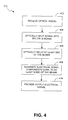
- the optical communication system 100 of FIG. 2 incorporates an electronic equalizer 202 that is adapted to perform electrical signal equalization. In such a system, the optical signals are converted to electrical signals and then equalized by the electronic equalizer.
- Systems and methods of the invention perform time-domain equalization of signals, at least partially, in the optical domain. In this manner, more precise delays can be introduced during equalization than achieved by conventional electrical equalization. Additionally, by optically introducing such delay, i.e., introducing the delay before the optical signal is converted to an electrical signal, transmission errors can be equalized before propagating farther downstream. By correcting the errors earlier, the errors may be less significant than if permitted to propagate farther before correction and, therefore, may be more effectively equalized.
- Systems of the invention can perform equalization by receiving an optical signal, such as via an optical fiber of an optical communication system.
- the optical signal is then split into multiple beams, with at least one of the beams being optically delayed relative to the others.
- the beams, or electrical signal components corresponding to the beams are then combined to produce an equalized output signal.
- the beams (signals) interfere with each other so that the output signal exhibits a more ideal shape compared to the received optical signal.
- a representative method for performing time-domain equalization of an information signal represented by an optical signal includes: receiving the optical signal; optically splitting the optical signal into beams; optically delaying at least one of the beams; detecting a plurality of the beams to generate respective electrical signal components; and summing a plurality of the electrical signal components to generate an electrical output signal representing the information signal.
- the detecting is performed before the scaling.
- some embodiments include scaling at least one of the signals (e.g., beams). This scaling can be performed electrically or optically.
- a representative system for performing time-domain equalization of an information signal represented by an optical signal includes a beamsplitter, a delay component, an array of photodetectors and an amplifier.
- the beamsplitter is adapted to split the optical signal optically into beams.
- the delay component which optically communicates with the beamsplitter, is configured to receive at least one of the beams and delay the at least one of the beams optically.
- the array of photodetectors is arranged to receive the at least one of the beams and is adapted to generate respective electrical signal components corresponding to the at least one of the beams.
- the amplifier is arranged to receive the electrical signal components and is adapted to generate an electrical output signal representing the information signal.
- FIG. 1 is a schematic diagram of a representative optical communication system of the prior art.
- FIG. 2 is a schematic diagram of the optical communication system of FIG. 1 showing detail of the receive components.
- FIG. 3 is a schematic diagram depicting an embodiment of the optical system of the present invention.
- FIG. 4 is a flowchart depicting functionality of an embodiment of the equalization system of FIG. 3.
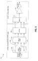
- FIG. 5 is a schematic diagram depicting an embodiment of the equalization system of FIG. 3.
- FIG. 6 is a flowchart depicting functionality of an embodiment of the equalization system of FIG. 3.
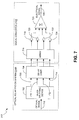
- FIG. 7 is a schematic diagram depicting another embodiment of the equalization of FIG. 3.
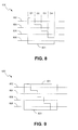
- FIG. 8 is a schematic diagram depicting an embodiment of a delay component that can be used in the equalization system of FIG. 3.
- FIG. 9 is a schematic diagram depicting another embodiment of a delay component that can be used in the equalization system of FIG. 3.
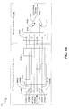
- FIG. 10 is a schematic diagram depicting another embodiment of the equalization system of FIG. 3.
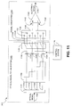
- FIG. 11 is a schematic diagram depicting still another embodiment of the equalization system of FIG. 3.
- FIG. 12 is a schematic diagram depicting yet another embodiment of the equalization system of FIG. 3.
- Optical systems of the present invention compensate for at least a portion of the impulse response impairments typically evident in optical circuits. This is achieved by incorporating one or more equalization systems that are adapted to equalize signals propagated via such optical circuits. As will be described in greater detail, equalization is achieved, at least in part, in the optical domain.
- FIG. 3 schematically depicts an optical system 300 of the present invention.
- optical system 300 defines an electrical domain 302 and an optical domain 304.
- Electrical domain 302 includes transmit components 306 and receive components 308.
- Transmit components 306 convert electrical signals into optical signals (pulses).
- Transmit components 306 provide the optical signals to optical circuit 310, which is associated with the optical domain.
- Optical system 300 also includes an equalization system 312 that receives the optical signals from optical circuit 310.
- Equalization system incorporates an optical equalization system 314 and a signal converter 316.
- the optical equalization system modifies the optical signals and provides the modified optical signals to signal converter 316.
- Signal converter 316 which can be considered one of the receive components, converts the modified optical signals to electrical signals.
- Receive components 308 then propagate the electrical signals to other components (not shown) of the optical system.
- FIG. 4 depicts the functionality of an embodiment of equalization system 312. It should be noted that in some alternative implementations, the functions noted in various blocks of FIG. 4 or any other of the accompanying flowcharts may occur out of the order in which they are depicted. For example, the respective functions of two blocks shown in succession in FIG. 4 may, in fact, be performed substantially concurrently. In other embodiments, the respective functions may be performed in the reverse order.
- functionality of the equalization system may be construed as beginning at block 402 where an optical signal is received.
- the optical signal is split optically into multiple beams.
- each of the multiple beams is a copy of the optical signal.
- at least one of the beams is delayed relative to the optical signal.
- all but one of the multiple beams can be delayed relative to the optical signal.
- the operations depicted in blocks 402 - 406 are preferably performed by optical equalization system 314 and, thus, are performed within the optical domain.
- electrical signal components corresponding to at least some of the beams are generated. Thereafter, such as depicted in block 410, an output electrical signal corresponding to the optical signal is provided.
- the output electrical signal is formed by combining, e.g., summing, the electrical signal components.
- signal components corresponding to the impulse response impairments of the received optical signal interfere with other signal components resulting in an output signal that exhibits a more ideal shape than the received optical signal.
- scaling of at least one of the beams and/or electrical signal components can be performed. For example, at least one of the beams can be optically scaled prior to being converted to a corresponding electrical signal component(s). Alternatively, at least one of the electrical signal components can be electrically scaled.
- equalization system 312 includes an optical equalization system 314A and a signal converter 316A.
- Optical equalization system 314A incorporates a beamsplitting device (or "beamsplitter") 502, a delay component 504 and an attenuator 506.
- the beamsplitting device, delay component and attenuator optically communicate to provide multiple beams to the signal converter.
- beamsplitting device 502 produces beams 508, 510, 512, and 514 in response to receiving an input optical signal (represented by arrow 515).
- each of the beams is a copy of the input optical signal. It should be noted that although four beams are depicted in FIG. 5, various other numbers of beams can be used.
- Beamsplitting device 502 provides beams 508, 510, 512, and 514 to delay component 504.
- delay component 504 differentially delays each of the beams and then provides the beams to attenuator 506.
- Attenuator 506 then optically scales the beams.
- the attenuator which is able to provide gains of 0 to +1, can selectively provide a fixed attenuation to each of the beams. Attenuation typically differs among the beams. In particular, at least one of the beams is scaled relative to the others.
- each beam is provided to signal converter 316A. More specifically, each of the beams is detected by a photodetector of array 516. An amplifier 518 receives the output electrical components of the photodetectors and then provides an output electrical signal 520 that corresponds to the input optical signal.
- functionality of the equalization system may be construed as beginning at block 602 where an optical signal is received.
- the optical signal is split optically into multiple beams.
- each of the multiple beams is a copy of the optical signal.
- at least one of the beams is delayed relative to the optical signal.
- all but one of the multiple beams can be delayed relative to the optical signal.
- the operations depicted in blocks 602 - 606 are preferably performed by optical equalization system 314 and, thus, are performed within the optical domain.
- electrical signal components corresponding to at least some of the beams are generated.
- at least one of the beams is scaled electrically.
- an output electrical signal corresponding to the optical signal is provided.
- the output electrical signal is formed by summing the electrical signal components.
- equalization system 312 includes an optical equalization system 314B and a signal converter 316B.
- Optical equalization system 314B incorporates a beamsplitting device 702, a delay component 704 and an array of photodetectors 716.
- the beamsplitting device and delay component optically communicate to provide multiple beams to the signal converter.
- beamsplitting device 702 produces beams 708, 710, 712, and 714 in response to receiving an input optical signal (represented by arrow 715).
- each of the beams is a copy of the input optical signal. It should be noted that although four beams are depicted in FIG. 7, various other numbers of beams can be used.
- Beamsplitting device 702 provides beams 708, 710, 712, and 714 to delay component 704.
- delay component 704 differentially delays each of the beams and then provides the beams to array 716. More specifically, each of the beams is detected by a photodetector of array 716 and is converted to a corresponding output electrical component.
- the output electrical components are received by scaling components, e.g. , amplifiers, 718, 720, 722 and 724, respectively.
- Each of the scaling components electrically scales a corresponding one of the output electrical components to provide a predetermined attenuation to each of the output electrical components. Attenuation typically differs among the output electrical components. In particular, at least one of the output electrical components is scaled relative to the others.
- a summing component 726 receives the scaled output electrical components and then provides an output electrical signal 728 that corresponds to the input optical signal. Note, selection of appropriate delays and attenuations can be made in a conventional manner.
- Various beamsplitting devices may be used to split an input optical signal into multiple beams.
- at least a portion of the delay to be provided to each beam also can be provided by the beamsplitting device.
- a combination reflective-refractive element can provide different path lengths along which each of the multiple beams propagate. Since the propagation velocity of light through the material of a combination reflective-refractive element is slower than the propagation velocity of light through free-space, an increased path length provides a corresponding increase in delay of the beam propagating along that path.
- DOE Diffractive optical elements
- a DOE uses interference and the wave property of light to split the input optical signal. Due to the potentially different path lengths associated with a DOE, delay also can be applied to one or more of the split beams by the DOE.
- Various delay components also may be used to delay one or more of the multiple beams split from an input optical signal.
- delay can be achieved through free-space path delays in some embodiments.
- free-space path delays the distance necessary to incorporate one bit period of delay in a beam decreases proportionally as signal bit rates increase. For example, at 10gbd the symbol rate is 100ps.
- a corresponding delay can be achieved by providing a path length difference of 3cm.
- the required free-space path delay can be physically shortened by using media other than air.
- beam folding techniques also can be utilized to shorten the required distance. For instance, in the 10gbd example, the required length can be reduced to under 1cm if the optical path includes one reflective fold and is contained within a typical transparent plastic media.
- the optical path can be defined, at least in part, by an optically transparent material with a velocity of propagation slower than that of free-space.
- delay component 800 includes a delay element 801 that is configured to receive multiple beams, e.g. , beams 802, 804, 806, and 808.
- element 801 exhibits a refractive index greater than one, beams having longer propagation paths through the element are delayed longer than beams having shorter propagation paths.
- beam 808 is delayed longer than 806, beam 806 is delayed longer beam 804, and beam 804 is delayed longer than beam 802.
- delay component 800 can be configured so as to accommodate various numbers of beams other than the number depicted. Additionally, as it may be desired in some embodiments to provide a reference beam that is not delayed, delay component 800 can be configured to accommodate propagation of one or more beams without providing a corresponding delay to that beam(s).
- delay component 800 includes a first delay element 801 and a second delay element 901.
- each element has a refractive index of greater than one (1), with the refractive index of the first element preferably being greater than the refractive index of the second element.
- an increase in delay of a particular beam may be provided by lengthening the path and/or by increasing the index of refraction of one or more materials of the delay component.
- delay component 800 may be considered mechanically advantageous.
- alignment of the component in an optical system may be more convenient, compared to aligning an embodiment such as that depicted in FIG. 8.
- the exterior surfaces of the delay component may be configured to engage corresponding alignment surfaces of the optical system.
- equalization system 312 includes an optical equalization system 314C and a signal converter 316C.
- the optical equalization system 314C includes a beamsplitting device 1002, a delay component 1004, and an attenuator 1006.
- An input optical signal, represented by arrow 1007, is provided to beamsplitting device 1002.
- beamsplitting device 1002 produces pairs of beams, e.g., pairs 1008A, 1008B, 1010A, 1010B, 1012A, 1012B, and 1014A, 1014B. Each of the pairs of beams is provided to and differentially delayed by delay component 1004.
- delay component 1004 provides an equivalent, predetermined delay to each beam of a pair of beams.
- the pairs of beams then are provided to attenuator 1006, which optically scales at least one of the beams.
- attenuator 1006 is configured to provide a fixed attenuation to each of the beams. In other embodiments, however, a control system may be used to impart a controlled attenuation to each beam.
- each beam is provided to and detected by a photodetector of array 1016. More specifically, the array 1016 includes pairs of detectors, with each pair including a detector 1018 and a detector 1020. Each detector 1018 is configured to receive light from the attenuator corresponding to a first or "A" beam of a beam pair. Each detector 1020 is configured to receive light corresponding to a second or "B" beam of a beam pair. Each pair of detectors 1018, 1020 differentially detects a corresponding pair of beams and produces corresponding pairs of output electrical components.
- An output electrical signal 1022 corresponding to the input optical signal is produced by amplifier 1024.
- electrical components output by the photodetector array representing positive coefficients can be provided to input 1026 of the amplifier and electrical components output by the photodetector array representing negative coefficients can be provided to input 1028.
- FIG. 11 A fourth embodiment that does not use an attenuator is depicted in FIG. 11.
- equalization system 512 includes a beamsplitting device 1102, a delay component 1104, a birefringent component 1106 and a walk-off crystal 1108.
- An input optical signal represented by arrow 1109, is provided to beamsplitting device 1102.
- beamsplitting device 1102 produces beams 1110, 1112, 1114, and 1116, which are provided to delay component 1004.
- Each of the beams is differentially delayed by delay component 1004, with a predetermined delay being provided to each beam.
- the liquid crystal cells e.g.
- cells 1118, 1120, 1122 and 1124 are adapted to impart an individually controllable rotation of the polarization plane upon each beam.
- Control of the rotation of the polarization plane preferably is provided by a control system 1126.
- a control system may not be used as the rotation of the polarization plane imparted upon each beam can be predetermined.
- the walk-off crystal splits each of the beams into a pair of beams, e.g. , beam 1110 is split into beams 1110A and 1110B.
- the relative intensity of each beam within each pair is determined by the rotation of polarization imparted on the beam by the birefringent component 1106, therefore, the birefringent component optically scales the beams.
- Each beam is then detected by an array 1130 of photodetectors. More specifically, the array 1130 includes pairs of detectors, with each pair including a first detector 1132 and a second detector 1134. The first detectors 1132 are positioned to receive light from the walk-off crystal resulting from no rotation of polarization by the birefringent component.
- the detectors 1132 correspond to a scaling coefficient of +1.
- the second detectors 1134 are positioned to receive light from the walk-off crystal resulting from 90° rotation of polarization by the birefringent component.
- the detectors 1134 correspond to a coefficient of -1.
- the first and second detectors produce output electrical components that are differentially detected by amplifier 1140.
- each pair of beams is converted to an electrical component that is differentially detected by the amplifier.
- the electrical components output by the photodetectors representing positive coefficients can be provided to input 1142 of the amplifier and the electrical components output by the photodetectors representing negative coefficients can be provided to input 1144.
- the amplifier then provides an electrical output signal 1150 that corresponds to the input optical signal.
- Control systems of the invention can be implemented in software, firmware, hardware, or a combination thereof.
- the control system can be implemented with any or a combination of various technologies.
- the following technologies which are each well known in the art, can be used: a discrete logic circuit(s) having logic gates for implementing logic functions upon data signals, an application specific integrated circuit (ASIC) having appropriate combinational logic gates, a programmable gate array(s) (PGA), and a field programmable gate array (FPGA).
- control system 1126 can be implemented in software as an executable program. Such a control system can be executed by a special or general purpose digital computer.
- control system 1126 may use one or more of a variety of such algorithms to tune the equalization system of the invention. For instance, the control system could use the Least Mean Squares (LMS) algorithm. When using this algorithm, the equalization system is tuned to minimize the mean square error between the received pulse and an "expected" pulse.
- LMS Least Mean Squares
- the equalization system can function as a fixed equalizer.
- components that provide predetermined delays and/or attenuations can be used.
- FIG. 12 depicts a fifth embodiment of the equalization system 312.
- the embodiment of FIG. 12 can be used to equalize an input optical signal when the polarization of the input optical signal is not known.
- equalization system 312 includes an optical equalization system 314E and a signal converter 316E.
- Optical equalization system 314E incorporates a polarization splitter 1202 that is adapted to receive an input optical signal 1204.
- the polarization splitter 1202 receives input optical signal 1204 and produces two output beams 1206A and 1206B, respectively. Each of the output beams exhibits a different plane of polarization with respect to the other.
- the output beams are provided to optical equalization components. More specifically, output beam 1206A is provided to first optical equalization components 1210A and output beam 1206B is provided to second optical equalization components 1210B.
- Each of the optical equalization components includes a beamsplitting device, a delay component, a birefringent component and a walk-off crystal (none of which are depicted in FIG. 12). These components were described before in relation to FIG. 11 and will not be described in detail here. Generally, however, each of the optical equalization components receives a corresponding output beam (1206A, 1206B) and then provides pairs of beams 1212A,1212B to an array 1214 of photodetectors. More specifically, the array 1214 includes pairs of detectors, with each pair including a first detector 1216 and a second detector 1218.
- the first detectors 1216 are positioned to receive light from the optical equalization components resulting from no rotation of polarization, and the second detectors 1218 are positioned to receive light from the optical equalization components resulting from 90° rotation of polarization.
- the first and second detectors produce output electrical components that are differentially detected by amplifier 1220.
- the amplifier then provides an electrical output signal 1222 that corresponds to the input optical signal.
- control of the rotation of the polarization plane preferably is provided by a control system, e.g ., control system 1126 of FIG. 11.
- a control system may not be used as the rotation of the polarization plane imparted upon each beam can be predetermined.
Landscapes
- Physics & Mathematics (AREA)
- Electromagnetism (AREA)
- Engineering & Computer Science (AREA)
- Computer Networks & Wireless Communication (AREA)
- Signal Processing (AREA)
- Optical Communication System (AREA)
- Cable Transmission Systems, Equalization Of Radio And Reduction Of Echo (AREA)
Abstract
Description
Claims (10)
- A method for performing time-domain equalization of an information signal represented by an optical signal, said method comprising:receiving the optical signal;optically splitting the optical signal into beams;optically delaying at least one of the beams;detecting a plurality of the beams to generate respective electrical signal components; andcombining a plurality of the electrical signal components to generate an electrical output signal representing the information signal.
- The method of claim 1, further comprising:optically scaling at least one of the beams.
- The method of claim 2, wherein, in detecting the plurality of the beams, at least one of the beams detected has not been subjected to at least one of (a) the delaying, and (b) the scaling.
- The method of any of claims 1 to 3, further comprising:electrically scaling at least one of the electrical signal components.
- The method of any of claims 1 to 4,wherein optically splitting the optical signal includes:providing a beamsplitter (502, 702, 1002, 1102, 1202); andperforming the splitting using the beamsplitter.
- The method of any of claims 1 to 4, wherein optically splitting the optical signal includes:providing a diffractive optical element; andperforming the splitting using the diffractive optical element.
- The method of claim 2, further comprising:providing a diffractive optical element; andperforming the splitting and the scaling using the diffractive optical element.
- A system for performing time-domain equalization of an information signal represented by an optical signal, said system comprising:a beamsplitter (502, 702, 1002, 1102, 1202) adapted to split the optical signal optically into beams;a delay component (504, 704, 800, 1004, 1104) optically communicating with the beamsplitter, the delay component being configured to receive at least one of the beams and delay the at least one of the beams optically;an array ofphotodetectors (516, 716, 1016, 1130) arranged to receive the at least one of the beams, the array of photodetectors being adapted to generate respective electrical signal components corresponding to the at least one of the beams; andan amplifier (518, 726, 1024, 1140, 1220) arranged to receive the electrical signal components, the amplifier being adapted to generate an electrical output signal representing the information signal.
- The system of claim 8, further comprising:an attentuator (506) optically communicating with the delay component and the array of photodetectors, the attenuator being configured to scale at least one of the beams and provide the at least one of the beams to the array of photodetectors after scaling.
- The system of claim 8, further comprising:an attentuator electrically communicating with the array of photodetectors and the amplifier, the attenuator being configured to scale at least one of the electrical signal components and provide the at least one of the electrical signal components to the amplifier after scaling.
Applications Claiming Priority (2)
| Application Number | Priority Date | Filing Date | Title |
|---|---|---|---|
| US7531 | 1998-01-15 | ||
| US10/007,531 US7272324B2 (en) | 2001-10-26 | 2001-10-26 | Equalization of optical signals |
Publications (3)
| Publication Number | Publication Date |
|---|---|
| EP1309114A2 true EP1309114A2 (en) | 2003-05-07 |
| EP1309114A3 EP1309114A3 (en) | 2004-04-07 |
| EP1309114B1 EP1309114B1 (en) | 2007-01-03 |
Family
ID=21726742
Family Applications (1)
| Application Number | Title | Priority Date | Filing Date |
|---|---|---|---|
| EP02020312A Expired - Lifetime EP1309114B1 (en) | 2001-10-26 | 2002-09-11 | Equalization of optical signals |
Country Status (4)
| Country | Link |
|---|---|
| US (1) | US7272324B2 (en) |
| EP (1) | EP1309114B1 (en) |
| JP (1) | JP2003188823A (en) |
| DE (1) | DE60217261T2 (en) |
Families Citing this family (6)
| Publication number | Priority date | Publication date | Assignee | Title |
|---|---|---|---|---|
| JPWO2006095411A1 (en) * | 2005-03-08 | 2008-08-14 | 富士通株式会社 | Optical space communication method, optical transmitter, optical receiver, and optical space communication system |
| US7769302B1 (en) * | 2007-03-13 | 2010-08-03 | At&T Intellectual Property Ii, L.P. | Method and apparatus for adjusting for polarization-induced, optical signal transients |
| US9496964B2 (en) * | 2015-03-16 | 2016-11-15 | Alcatel-Lucent Usa Inc. | Optoelectronic equalizer circuit |
| KR102212297B1 (en) * | 2015-11-18 | 2021-02-04 | 럭스테라 엘엘씨 | Method and system for a distributed optoelectronic receiver |
| WO2019036303A1 (en) | 2017-08-12 | 2019-02-21 | Luxtera, Inc. | Method and system for waveguide delay based equalization with optical splitting in optical communication |
| CN115412175A (en) * | 2021-05-26 | 2022-11-29 | 华为技术有限公司 | Optical equalization equipment, receiving equipment and communication system |
Family Cites Families (14)
| Publication number | Priority date | Publication date | Assignee | Title |
|---|---|---|---|---|
| US3988624A (en) * | 1971-03-15 | 1976-10-26 | Eaton Corporation | Self-gauging sensor assembly |
| DE2432718A1 (en) | 1974-07-08 | 1976-01-29 | Siemens Ag | Long distance wideband transmission of optical signals - using multiple mode fibres laid in approx. straight line |
| US3988614A (en) | 1975-06-30 | 1976-10-26 | Northern Electric Company Limited | Equalization of chromatic pulse dispersion in optical fibres |
| DE3034640A1 (en) * | 1980-09-13 | 1982-05-06 | Philips Patentverwaltung Gmbh, 2000 Hamburg | ARRANGEMENT FOR RECOGNIZING A BINARY WORD |
| DE3212590A1 (en) | 1982-04-03 | 1983-10-13 | Wandel & Goltermann Gmbh & Co, 7412 Eningen | Method and device for the optical equalisation of signals being transmitted via optical fibres |
| JPH04280522A (en) * | 1991-03-08 | 1992-10-06 | Nec Corp | Optical connector and its drive method |
| GB9127057D0 (en) * | 1991-12-20 | 1992-02-19 | Secr Defence | Improved digital sampling of individual pulses |
| US5822100A (en) * | 1996-06-26 | 1998-10-13 | Mci Communications Corporation | Method and system for equalizing PMD using incremental delay switching |
| US6271952B1 (en) * | 1998-08-18 | 2001-08-07 | Nortel Networks Limited | Polarization mode dispersion compensation |
| US6708003B1 (en) * | 1999-12-16 | 2004-03-16 | Northrop Grumman Corporation | Optical energy transmission system utilizing precise phase and amplitude control |
| US6256103B1 (en) * | 2000-02-17 | 2001-07-03 | Agilent Technologies, Inc. | System and method for optical heterodyne detection of an optical signal |
| US6950611B2 (en) * | 2000-03-08 | 2005-09-27 | Fitel Usa Corp. | In-line polarization monitoring and control in lightwave communication systems |
| FR2818838A1 (en) | 2000-12-21 | 2002-06-28 | Cit Alcatel | ADJUSTABLE DIFFERENTIAL GROUP DELAY GENERATOR AND POLARIZATION DISPERSION COMPENSATOR INCORPORATING SAME |
| EP1306987A1 (en) * | 2001-10-23 | 2003-05-02 | Pro Forma Alfa | Spectrometer |
-
2001
- 2001-10-26 US US10/007,531 patent/US7272324B2/en not_active Expired - Fee Related
-
2002
- 2002-09-11 DE DE60217261T patent/DE60217261T2/en not_active Expired - Lifetime
- 2002-09-11 EP EP02020312A patent/EP1309114B1/en not_active Expired - Lifetime
- 2002-10-07 JP JP2002293604A patent/JP2003188823A/en not_active Withdrawn
Also Published As
| Publication number | Publication date |
|---|---|
| US7272324B2 (en) | 2007-09-18 |
| EP1309114A3 (en) | 2004-04-07 |
| JP2003188823A (en) | 2003-07-04 |
| US20030081291A1 (en) | 2003-05-01 |
| DE60217261D1 (en) | 2007-02-15 |
| EP1309114B1 (en) | 2007-01-03 |
| DE60217261T2 (en) | 2007-06-21 |
Similar Documents
| Publication | Publication Date | Title |
|---|---|---|
| US8478135B2 (en) | Method and apparatus for polarization-division-multiplexed optical receivers | |
| EP2521289B1 (en) | Optical receiver for multimode communications | |
| US10554311B2 (en) | Method and system for waveguide delay based equalization with optical splitting in optical communication | |
| US10439734B2 (en) | Method and system for waveguide delay based equalization with summing at single-ended to differential converters in optical communication | |
| EP1460788B1 (en) | Multi-channel optical equalizer for intersymbol interference mitigation | |
| US20030223689A1 (en) | System for higher-order dispersion compensation including phase modulation | |
| EP3358767A1 (en) | Device and method for processing light signal | |
| US9831957B2 (en) | Self-equalizing photo detector | |
| EP1380828A1 (en) | Optoelectronic module with integrated loop-back capability | |
| CN102308499B (en) | Optical communication system and optical communication method | |
| EP1309114B1 (en) | Equalization of optical signals | |
| US11290184B2 (en) | Switchable dispersion compensating module | |
| US20200177285A1 (en) | Method and system for waveguide delay based equalization with current and optical summing in optical communication | |
| US20030235145A1 (en) | Crosstalk compensation engine for reducing signal crosstalk effects within a data signal | |
| US8923460B1 (en) | Methods and apparatus for signal equalization in dual polarization multiplexed optical communication systems | |
| US7254343B2 (en) | Method and apparatus for data recovery in an optical transmission system | |
| US8170424B2 (en) | Method and apparatus for optical signal power discrimination | |
| US7088925B1 (en) | Device for detecting polarization mode dispersion | |
| US20100061738A1 (en) | Signal Processor for Compensating for Optical Fiber Chromatic Dispersion | |
| CN101517939A (en) | Optical regenerator and phase error detection unit for an optical regenerator and method for optical regeneration | |
| US20040208626A1 (en) | Coherent equalization of optical signals | |
| JP5658610B2 (en) | Optical fiber transmission system and optical receiver | |
| US6580857B1 (en) | Apparatus for reshaping optical pulses | |
| RU2778554C1 (en) | Method for compensation for optical signal dispersion distortion in multimode fiber-optic transmission lines | |
| JPH1172811A (en) | Optical signal processing method and optical transversal filter |
Legal Events
| Date | Code | Title | Description |
|---|---|---|---|
| PUAI | Public reference made under article 153(3) epc to a published international application that has entered the european phase |
Free format text: ORIGINAL CODE: 0009012 |
|
| AK | Designated contracting states |
Designated state(s): AT BE BG CH CY CZ DE DK EE ES FI FR GB GR IE IT LI LU MC NL PT SE SK TR |
|
| AX | Request for extension of the european patent |
Extension state: AL LT LV MK RO SI |
|
| PUAL | Search report despatched |
Free format text: ORIGINAL CODE: 0009013 |
|
| AK | Designated contracting states |
Kind code of ref document: A3 Designated state(s): AT BE BG CH CY CZ DE DK EE ES FI FR GB GR IE IT LI LU MC NL PT SE SK TR |
|
| AX | Request for extension of the european patent |
Extension state: AL LT LV MK RO SI |
|
| 17P | Request for examination filed |
Effective date: 20040805 |
|
| 17Q | First examination report despatched |
Effective date: 20040909 |
|
| AKX | Designation fees paid |
Designated state(s): DE GB |
|
| GRAP | Despatch of communication of intention to grant a patent |
Free format text: ORIGINAL CODE: EPIDOSNIGR1 |
|
| GRAS | Grant fee paid |
Free format text: ORIGINAL CODE: EPIDOSNIGR3 |
|
| GRAA | (expected) grant |
Free format text: ORIGINAL CODE: 0009210 |
|
| RAP1 | Party data changed (applicant data changed or rights of an application transferred) |
Owner name: AVAGO TECHNOLOGIES FIBER IP (SINGAPORE) PTE. LTD. |
|
| AK | Designated contracting states |
Kind code of ref document: B1 Designated state(s): DE GB |
|
| REG | Reference to a national code |
Ref country code: GB Ref legal event code: FG4D |
|
| REF | Corresponds to: |
Ref document number: 60217261 Country of ref document: DE Date of ref document: 20070215 Kind code of ref document: P |
|
| PLBE | No opposition filed within time limit |
Free format text: ORIGINAL CODE: 0009261 |
|
| STAA | Information on the status of an ep patent application or granted ep patent |
Free format text: STATUS: NO OPPOSITION FILED WITHIN TIME LIMIT |
|
| 26N | No opposition filed |
Effective date: 20071005 |
|
| REG | Reference to a national code |
Ref country code: DE Ref legal event code: R082 Ref document number: 60217261 Country of ref document: DE Representative=s name: DILG HAEUSLER SCHINDELMANN PATENTANWALTSGESELL, DE |
|
| REG | Reference to a national code |
Ref country code: DE Ref legal event code: R081 Ref document number: 60217261 Country of ref document: DE Owner name: AVAGO TECHNOLOGIES GENERAL IP (SINGAPORE) PTE., SG Free format text: FORMER OWNER: AVAGO TECHNOLOGIES FIBER IP (SINGAPORE) PTE. LTD., SINGAPORE, SG Effective date: 20130628 Ref country code: DE Ref legal event code: R082 Ref document number: 60217261 Country of ref document: DE Representative=s name: DILG HAEUSLER SCHINDELMANN PATENTANWALTSGESELL, DE Effective date: 20130628 |
|
| PGFP | Annual fee paid to national office [announced via postgrant information from national office to epo] |
Ref country code: DE Payment date: 20150820 Year of fee payment: 14 Ref country code: GB Payment date: 20150825 Year of fee payment: 14 |
|
| REG | Reference to a national code |
Ref country code: DE Ref legal event code: R119 Ref document number: 60217261 Country of ref document: DE |
|
| GBPC | Gb: european patent ceased through non-payment of renewal fee |
Effective date: 20160911 |
|
| PG25 | Lapsed in a contracting state [announced via postgrant information from national office to epo] |
Ref country code: DE Free format text: LAPSE BECAUSE OF NON-PAYMENT OF DUE FEES Effective date: 20170401 Ref country code: GB Free format text: LAPSE BECAUSE OF NON-PAYMENT OF DUE FEES Effective date: 20160911 |