EP1309085A1 - Surface acoustic wave device and substrate thereof - Google Patents
Surface acoustic wave device and substrate thereof Download PDFInfo
- Publication number
- EP1309085A1 EP1309085A1 EP01932282A EP01932282A EP1309085A1 EP 1309085 A1 EP1309085 A1 EP 1309085A1 EP 01932282 A EP01932282 A EP 01932282A EP 01932282 A EP01932282 A EP 01932282A EP 1309085 A1 EP1309085 A1 EP 1309085A1
- Authority
- EP
- European Patent Office
- Prior art keywords
- layer
- intermediate layer
- acoustic
- wave device
- diamond
- Prior art date
- Legal status (The legal status is an assumption and is not a legal conclusion. Google has not performed a legal analysis and makes no representation as to the accuracy of the status listed.)
- Withdrawn
Links
Images
Classifications
-
- H—ELECTRICITY
- H03—ELECTRONIC CIRCUITRY
- H03H—IMPEDANCE NETWORKS, e.g. RESONANT CIRCUITS; RESONATORS
- H03H9/00—Networks comprising electromechanical or electro-acoustic elements; Electromechanical resonators
- H03H9/25—Constructional features of resonators using surface acoustic waves
-
- H—ELECTRICITY
- H03—ELECTRONIC CIRCUITRY
- H03H—IMPEDANCE NETWORKS, e.g. RESONANT CIRCUITS; RESONATORS
- H03H9/00—Networks comprising electromechanical or electro-acoustic elements; Electromechanical resonators
- H03H9/02—Details
- H03H9/02535—Details of surface acoustic wave devices
- H03H9/02543—Characteristics of substrate, e.g. cutting angles
- H03H9/02582—Characteristics of substrate, e.g. cutting angles of diamond substrates
-
- H—ELECTRICITY
- H03—ELECTRONIC CIRCUITRY
- H03H—IMPEDANCE NETWORKS, e.g. RESONANT CIRCUITS; RESONATORS
- H03H9/00—Networks comprising electromechanical or electro-acoustic elements; Electromechanical resonators
- H03H9/02—Details
- H03H9/02535—Details of surface acoustic wave devices
- H03H9/02543—Characteristics of substrate, e.g. cutting angles
- H03H9/02574—Characteristics of substrate, e.g. cutting angles of combined substrates, multilayered substrates, piezoelectrical layers on not-piezoelectrical substrate
Definitions
- the present invention relates to a surface-acoustic-wave device that can be used in a high-frequency band, and a substrate suitably used for such a surface-acoustic-wave device.
- a surface-acoustic-wave (SAW) device utilizing a SAW which propagates in the surface of a solid body, satisfies properties required for an electromechanical functional part, such as ease in automating and simplifying its mounting operation, since it is small in size and light in weight, is superior in resistance against vibration and impact, and eliminates need for circuit adjustment.
- a SAW device has other various advantageous features, such as superior temperature stability, a long life, and superior phase characteristics. Therefore, SAW devices are widely employed as frequency filters, resonators, delay devices, Fourier transformers, convolvers, correlators, optoelectronic functional devices, etc.
- a SAW device having a multilayered structure composed of diamond and piezoelectric layers has come into wide use for applications in such a high-frequency band.
- a method for manufacturing such a SAW device comprises the steps of forming a diamond film by vapor-phase synthesis on a base film made of a material such as Si, polishing the surface of the diamond film into a smooth surface, and forming a piezoelectric layer and inter-digital transducers (IDTs) on the smooth surface, for example.
- the piezoelectric layer As for the piezoelectric layer, attention was given to a layer made of ZnO in the past. Recently, however, piezoelectric layers made of LiNbO 3 and LiTaO 3 have received attention.
- the piezoelectric layers made of LiNbO 3 and LiTaO 3 are superior in chemical stability, such as resistance against acids and alkalis, to those made of ZnO.
- LiNbO 3 has a higher electro-mechanical coupling coefficient (K 2 ) that is a guideline representing easiness in SAW excitation, and is suitably used in a wide-band filter for cellular phones, etc.
- Japanese Unexamined Patent Application Publication No. 8-154033 discloses a SAW device that has overcome the above problem.
- the SAW device disclosed in the Publication has been made based on the finding that the above-mentioned problem was attributable to improper crystal characteristics of LiNbO 3 .
- the disclosed SAW device has, between a diamond layer and a LiNbO 3 layer, an intermediate layer made of ZnO, Al 2 O 3 , MgO or the like.
- the intermediate layer has the function of controlling crystal characteristics (such as crystallinity and crystal direction) of the LiNbO 3 layer so that the characteristics of the SAW device are improved.
- a SAW device including a piezoelectric layer made of LiNbO 3 or LiTaO 3 has the following shortcoming.
- the intermediate layer between the diamond layer and the LiNbO 3 layer is formed of an oxide such as ZnO or MgO, the intermediate layer and the diamond layer are apt to separate from each other.
- the present invention has been made with the view of solving such problem, and its object is to provide a substrate for a surface-acoustic-wave device in which a diamond layer and an intermediate layer for controlling crystal characteristics of a piezoelectric layer do not separate easily from each other, and a surface-acoustic-wave device using such substrate.
- a substrate for a surface-acoustic-wave device is featured in comprising a diamond layer, an intermediate layer disposed on the diamond layer, and a piezoelectric layer disposed on the intermediate layer, the piezoelectric layer being made of LiNbO 3 , the intermediate layer being made of AlN.
- a SiO 2 layer is disposed on the piezoelectric layer.
- the SiO 2 layer By so disposing the SiO 2 layer on the piezoelectric layer, it is possible to stabilize temperature characteristics of the surface-acoustic-wave device and to prevent a variation of center frequency. This is because the temperature coefficient of SiO 2 has a sign opposite to signs of the temperature coefficients of LiNbO 3 and diamond, and a canceling effect results.
- the intermediate layer is made of AIN having C-axis orientation. Since the piezoelectric layer located on the intermediate layer has a tendency to follow the crystal characteristics of the intermediate layer, the piezoelectric layer can easily be made to have C-axis orientation by causing the intermediate layer to have C-axis orientation.
- the intermediate layer has a thickness of 5 to 100 nm. The reason is that if the intermediate layer is thinner than the lower limit of the above range, the function of controlling the crystal characteristics of the piezoelectric layer tends to be insufficient, and if the intermediate layer is thicker than the upper limit of the above range, the intermediate layer is more apt to impede the characteristics of the underlying diamond layer.
- the piezoelectric layer is made of LiNbO 3 having C-axis orientation.
- the piezoelectric layer of LiNbO 3 having C-axis orientation, piezoelectric characteristics can be improved.
- a surface-acoustic-wave device comprises the above-mentioned substrate for a surface-acoustic-wave device and exciting electrodes for exciting a surface acoustic wave.
- the intermediate layer is made of AlN as described above, and accordingly higher adhesion is achieved between the intermediate layer and the diamond layer in the substrate of the surface-acoustic-wave device, the resistance against vibration and impact can be improved.
- the inventors have also found that using AlN as the intermediate layer is very effective in improving adhesion between the diamond layer and the intermediate layer in the case of forming the piezoelectric layer of LiTaO 3 as with the case of using LiNbO 3 .
- a substrate for a surface-acoustic-wave device comprises a diamond layer, an intermediate layer disposed on the diamond layer, and a piezoelectric layer disposed on the intermediate layer, the piezoelectric layer being made of LiTaO 3 , the intermediate layer being made of AlN.
- a SiO 2 layer is disposed on the piezoelectric layer.
- the intermediate layer is made of AlN having C-axis orientation. Since the piezoelectric layer located on the intermediate layer has a tendency to follow the crystal characteristics of the intermediate layer, the piezoelectric layer can easily be made to have C-axis orientation by causing the intermediate layer to have C-axis orientation.
- the intermediate layer has a thickness of 5 to 100 nm. The reason is that if the intermediate layer is thinner than the lower limit of the above range, the function of controlling the crystal characteristics of the piezoelectric layer tends to be insufficient, and if the intermediate layer is thicker than the upper limit of the above range, the intermediate layer is more apt to impede the characteristics of the underlying diamond layer.
- the piezoelectric layer is made of LiTaO 3 having C-axis orientation.
- the piezoelectric layer of LiTaO 3 having C-axis orientation, piezoelectric characteristics can be improved.
- a surface-acoustic-wave device comprises the above-mentioned substrate for a surface-acoustic-wave device and exciting electrodes for exciting a surface acoustic wave.
- the intermediate layer is made of AlN as described above, and accordingly higher adhesion is achieved between the intermediate layer and the diamond layer in the substrate of the surface-acoustic-wave device, the resistance against vibration and impact can be improved.
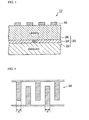
- 10 denotes a surface-acoustic-wave device, 20 a surface-acoustic-wave device substrate, 22 a diamond layer, 24 an intermediate layer (AlN), 26 a piezoelectric layer (LANbO 3 , LiTaO 3 ), 28 a SiO 2 layer, 30 an exciting electrode, and 32 a receiving electrode.
- a surface-acoustic-wave device 20 a surface-acoustic-wave device substrate, 22 a diamond layer, 24 an intermediate layer (AlN), 26 a piezoelectric layer (LANbO 3 , LiTaO 3 ), 28 a SiO 2 layer, 30 an exciting electrode, and 32 a receiving electrode.
- Fig. 1 is a sectional view showing a surface-acoustic-wave device (SAW device) 10 of this embodiment.
- the SAW device 10 is constituted by disposing, on a surface-acoustic-wave device substrate 20, exciting electrodes 30 for exciting surface acoustic waves (SAW).
- the surface-acoustic-wave device substrate 20 comprises a diamond layer 22, an intermediate layer 24 formed on the diamond layer 22, and a piezoelectric layer 26 made of LaNbO 3 and formed on the intermediate layer 24.
- the diamond layer 22 may be made of single-crystal diamond or poly-crystal diamond.
- the plane azimuth of the diamond layer 22 is not limited to a particular one and may be any one of (111), (100), (110), etc., for example, or these plane azimuths may exist in a mixed manner. Alternatively, those plane azimuths may exist in a mixed manner.
- the thickness of the diamond layer 22 is preferably not less than 5 ⁇ m and more preferably not less than 20 ⁇ m or not less than twice a wavelength, in view of easiness in the excitation of a surface acoustic wave.
- the diamond layer 22 may be formed on a substrate made of a semiconductor such as Si, or metal, glass, ceramic, or the like.
- the diamond layer 22 can be formed by any of various suitable methods. More specifically, there are a CVD (chemical vapor deposition) method, a microwave plasma CVD method, a PVD (physical vapor deposition) method, a sputtering method, an ion plating method, a plasma jet method, a flame method, a thermal filament method, etc.
- CVD chemical vapor deposition
- PVD physical vapor deposition
- the intermediate layer 24 may be formed directly on the diamond layer 22 which has been formed by any of those methods.
- the surface of the diamond layer 22 is preferably polished using, e.g., an electrodeposited diamond grindstone.
- the intermediate layer 24 has the function of controlling crystal characteristics of the piezoelectric layer 26 located on the intermediate layer 24, and is made of AlN in this embodiment. The inventors have found that adhesion between the diamond layer 22 and the intermediate layer 24 is improved by using AlN to form the intermediate layer 24.
- the intermediate layer 24 made of AlN preferably has C-axis orientation. Because the piezoelectric layer 26 located on the intermediate layer 24 has a tendency to follow the crystal characteristics of the intermediate layer 24, the piezoelectric layer 26 is easily made to have C-axis orientation by causing the intermediate layer 24 to have C-axis-orientation.
- the orientation of the intermediate layer 24 can be evaluated based on, e.g., the ⁇ -2 ⁇ method. For evaluating the orientation based on the ⁇ -2 ⁇ method, a sample to be measured is first put in a sample holder of an X-ray diffractometer. Then, X-ray diffraction peaks of the sample are measured based on the ⁇ -2 ⁇ method by using an X-ray diffraction pattern process.
- a total intensity (I C ) of all diffraction peaks corresponding to C-axis-oriented planes, i.e., (00m) planes (m integer not less than 1), and a total intensity (I T ) of all diffraction peaks are determined.
- a ratio (I C /I T ) between the two total peak intensities is preferably not less than 80 % and more preferably not less than 95 %.
- the thickness of the intermediate layer 24 can be selected as appropriate depending on the type of the underlying diamond layer 22, the size, the purpose of use, etc., but it is preferably in the range of 5 to 100 nm. The reason is that if the thickness of the intermediate layer 24 is smaller than the above range, the function of controlling the crystal characteristics of the piezoelectric layer 26 tends to become insufficient, and if the thickness of the intermediate layer 24 is larger than the above range, the electro-mechanical coupling coefficient (K 2 ) is reduced and accordingly it is difficult to excite a surface acoustic wave. Further, the thickness of the intermediate layer 24 is preferably selected such that the piezoelectric layer 26 made of LiNbO 3 has C-axis orientation with ease. Incidentally, the thickness of the intermediate layer 24 can be determined by observing a cut surface of the surface-acoustic-wave device substrate 20 with a film thickness measuring device, e.g., a scanning electron microscope (SEM).
- SEM scanning electron microscope
- the intermediate layer 24 preferably has an insulation level such that its resistivity is not less than about 10 4 ⁇ cm. The reason is that if the resistivity of the intermediate layer 24 is lower than such a level, the conductivity becomes high, which will cause power loss.
- a method of forming the intermediate layer 24 is not limited to a particular one, and may be any of well-known various vapor-phase deposition processes such as CVD, PVD, sputtering and ion plating.
- the piezoelectric layer 26, which is made of LiNbO 3 as mentioned above, may be a single crystal or poly-crystal. Also, the thickness of the piezoelectric layer 26 is not limited in particular, and can be selected as appropriate depending on the use of the surface-acoustic-wave device substrate 20 or the SAW device 10.
- the piezoelectric layer 26 is preferably formed of LiNbO 3 having C-axis orientation.
- the crystal characteristics (such as crystallinity and crystal direction) of the piezoelectric layer 26 have a tendency to follow the crystal characteristics of the underlying intermediate layer 24.
- the piezoelectric layer 26 can be more easily C-axis-orientated by causing the intermediate layer 24 to have C-axis orientation.
- a method of forming the piezoelectric layer 26 made of LiNbO 3 is not limited to a particular one, and may be any of well-known various vapor-phase deposition processes such as sputtering, vapor deposition, CVD, laser abrasion, MOCVD (metal-organic chemical vapor deposition), and MBE (molecular beam epitaxy).
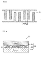
- Fig. 2 is a plan view of the exciting electrodes provided on the SAW device 10 shown in Fig. 1.
- the exciting electrodes 30 are constituted as the so-called single-type interdigital transducers.
- Materials of the exciting electrodes 30 are not limited to particular ones, but are preferably selected from Al, Al-Cu, Al-Si-Cu, and so on in consideration of machinability and cost.
- the thickness of the exciting electrodes 30 may be set to any desired range so long as the exciting electrodes 30 can develop the function of exciting a surface acoustic wave, but it is preferably in the range of about 10 to 500 nm.
- the reason why the electrode thickness is preferably in the above range is that if the thickness of the exciting electrodes 30 is less than 10 nm, the resistivity becomes high, resulting in an increased loss, and if the thickness of the exciting electrodes 30 exceeds 500 nm, the mass effect of the electrodes upon producing SAW reflection is noticeable and the desired SAW characteristics would be impeded.
- the exciting electrodes 30 are formed as the single-type interdigital transducers, they may be constituted as the so-called double-type interdigital transducers shown in Fig. 3. Also, the exciting electrodes 30 may be disposed such that they are buried in the surface of the underlying layer (e.g., the surface of the piezoelectric layer 26). More specifically, by way of example, recessed grooves are formed in the surface of the piezoelectric layer 26, and a conductive material, such as Al, which constitutes the exciting electrodes 30, is wholly or partially buried in the grooves.
- the height of the exciting electrodes 30 can be made almost equal to that of the surface in which the exciting electrodes 30 are to be formed. Consequently, it is possible to reduce the effect caused by the exciting electrodes upon SAW reflection.
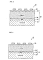
- the exciting electrodes 30 may be formed between the diamond layer 22 and the intermediate layer 24 as shown in Fig. 4, or may be formed between the intermediate layer 24 and the piezoelectric layer 26 (though not shown). However, from the viewpoint of not impeding the function of the intermediate layer 24 to control the crystal characteristics of the piezoelectric layer 26, the exciting electrodes 30 are preferably formed at the position shown in Fig. 1. Also, in the case where the exciting electrodes 30 are formed from a metal having a relatively low melting point, such as Al, etc., the exciting electrodes 30 are preferably formed on the piezoelectric layer 26 as shown in Fig. 1, rather than being formed between the diamond layer 22 and the intermediate layer 24 as shown in Fig.
- the thickness of the exciting electrodes 30 is preferably smaller than that of the intermediate layer 24 and more preferably not greater than 1/2 (in particular not greater than 1/5) of that of the intermediate layer 24.
- the SAW device 10 of this embodiment may include a SiO 2 layer 28 formed on the piezoelectric layer 26.
- the SiO 2 layer 28 By so forming the SiO 2 layer 28 on the piezoelectric layer 26, it is possible to stabilize temperature characteristics of the surface-acoustic-wave device 10 and to prevent a variation of center frequency. This is because the temperature coefficient of the SiO 2 layer 28 has a sign opposite to the signs of the temperature coefficients of LiNbO 3 of the piezoelectric layer 26 and the diamond layer 22, whereby a canceling effect results.
- the SiO 2 layer 28 is preferably formed of an amorphous film.
- the SAW device 10 of this embodiment may include a short-circuit electrode (not shown) formed as required.
- the short-circuit electrode serves as an electrode for changing the SAW characteristics of the SAW device 10 by forming an equi-potential surface.
- the short-circuit electrode preferably has a planar form occupying an area which is substantially the same proportion as, for example, the exciting electrode 30.
- the short-circuit electrode is preferably formed of a metal film, such as Al, Au, Al-Cu or Al-Si-Cu. Since the short-circuit electrode has the function different from that of the exciting electrode 30, it may be formed using a different material from that of the exciting electrode 30.
- the short-circuit electrode may be disposed at any position: on the piezoelectric layer 26, or between the diamond layer 22 and the intermediate layer 24, or between the intermediate layer 24 and the piezoelectric layer 26.
- the short-circuit electrode is preferably disposed on an opposite side of the exciting electrode 30 relative to the piezoelectric layer 26 such that the piezoelectric layer 26 is located between the short-circuit electrode and the exciting electrode 30.
- the short-circuit electrode is preferably disposed on the piezoelectric layer 26 or between the diamond layer 22 and the intermediate layer 24.
- the thickness of the short-circuit electrode is not limited in particular so long as the function of the short-circuit electrode can be developed, but it is preferably in the range of about 5 to 300 nm.
- the reason why the electrode thickness should preferably be in that range is that if the short-circuit electrode is thinner than 5 nm, it would be difficult to form an equi-potential surface, and if the short-circuit electrode is thicker than 300 nm, the short-circuit electrode more easily affects SAW reflection.
- the intermediate layer 24 is made of AlN, adhesion between the diamond layer 22 and the intermediate layer 24 can be improved. Consequently, the surface-acoustic-wave device 10 has improved resistance against vibration and impact.
- Fig. 6 shows a second embodiment of the surface-acoustic-wave device substrate 20 and the surface-acoustic-wave device 10 according to the present invention.
- This second embodiment differs from the first embodiment in that the piezoelectric layer 26 is made of LiTaO 3 instead of LiNbO 3 .
- the diamond layer 22, the intermediate layer 24 and the exciting electrodes 30 can be set to have the same shape, size, material, orientation, etc. as those in the first embodiment, respectively, except for the piezoelectric layer 26.
- crystal characteristics of the piezoelectric layer 26 are determined depending on those of the underlying intermediate layer 24.
- crystal characteristics of the piezoelectric layer 26 made of LiTaO 3 are controlled by the intermediate layer 24.
- LiTaO 3 forming the piezoelectric layer 26 may be a single-crystal or poly-crystal. However, to improve piezoelectric characteristics of the SAW device 10, the piezoelectric layer 26 is preferably formed of LiTaO 3 having C-axis orientation.
- a method of forming the piezoelectric layer 26 made of LiTaO 3 is not limited to a particular one, and may be any of well-known various vapor-phase deposition processes such as sputtering, vapor deposition, CVD, laser abrasion, MOCVD (metal-organic chemical vapor deposition), and MBE (molecular beam epitaxy).
- the SiO 2 layer 28 may be formed on the piezoelectric layer 26, and a short-circuit electrode may be formed in an appropriate place.
- the intermediate layer 24 is made of AlN as in the first embodiment, the adhesion between the diamond layer 22 and the intermediate layer 24 can be improved. Consequently, the resistance against vibration and impact is also improved in the surface-acoustic-wave device 10.
- a diamond film with a thickness of about 35 ⁇ m was grown on a Si base plate by microwave plasma CVD using a hydrogen gas with a 2% methane concentration. Film growth conditions in that step were as follows.
- the diamond film was mechanically polished using an electrodeposited diamond grindstone, whereby a multilayered structure of diamond/Si base plate with the diamond film having a thickness of 20 ⁇ m was obtained.
- an intermediate layer made of AlN was formed on the multilayered structure of diamond/Si base plate by RF magnetron sputtering.
- the intermediate layer had a thickness of 5 to 100 nm.
- Film growth conditions in that step were as follows.
- the thickness of the AlN intermediate layer was measured using a SEM.
- the thickness of the intermediate layer was not more than 5 nm, no peaks were found.
- a piezoelectric film of LiNbO 3 was formed by sputtering on the multilayered structure of AlN intermediate layer/diamond film/Si base plate thus obtained, whereby a surface-acoustic-wave device substrate according to the present invention was obtained.
- the film thickness of LiNbO 3 was adjusted such that a total film thickness of the LiNbO 3 piezoelectric layer and the AlN intermediate layer was 670 nm.
- Growth conditions for the LiNbO 3 piezoelectric layer were as follows.
- the thickness of the LiNbO 3 piezoelectric film was measured using a SEM.
- the formed piezoelectric layer showed no particular orientation.
- an Al layer with a thickness of 50 nm was formed by resistance-heating vapor deposition at a deposition rate of 5 nm/sec (substrate temperature: room temperature).
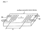
- a SAW device as shown in Fig. 7 was thereby completed.
- the Al electrodes thus formed were the exciting electrodes 30 for exciting a SAW and receiving electrodes 32 for receiving the SAW.
- the number of electrode pairs of the exciting electrodes 30 and the receiving electrodes 32 was set to 40, and a center-to-center distance X between the two types of electrodes was set to 600 ⁇ m.
- wire-bonding of Al wires (diameter of 30 ⁇ m) was provided through pads to the exciting electrodes 30 and the receiving electrodes 32.
- the wire was cut at its neck portion when the tensile strength of about 5 kgf to about 8 kgf was applied. From those results, it was confirmed that the SAW device with the intermediate layer made of AlN had higher adhesion to the diamond layer.
- a SAW device with the piezoelectric layer made of LiTaO 3 was fabricated. Growth conditions for the LiTaO 3 piezoelectric layer were given below. Note that since the diamond layer, the AlN intermediate layer, and the exciting electrodes on the piezoelectric layer were formed under the same conditions as those in Example 1, they are not described here.
- the wires were broken at the neck portion when the tensile strength of about 5 kgf to about 8 kgf was applied. From those results, it was confirmed that the SAW device with the intermediate layer made of AlN had higher adhesion to the diamond layer.
Landscapes
- Physics & Mathematics (AREA)
- Acoustics & Sound (AREA)
- Surface Acoustic Wave Elements And Circuit Networks Thereof (AREA)
Abstract
Provided are a substrate for a surface-acoustic-wave device and a
surface-acoustic-wave device, in which an intermediate layer for controlling
crystal characteristics of a piezoelectric layer does not easily separate from a
diamond layer.
A surface-acoustic-wave device substrate 20 and a surface-acoustic-wave
device 10, according to the present invention, comprises a diamond layer 22,
an intermediate layer 24 disposed on the diamond layer 22, and a piezoelectric
layer 26 disposed on the intermediate layer 24, the piezoelectric layer 26 being
made of LiNbO3 or LiTaO3, the intermediate layer 24 being made of AlN.
Description
The present invention relates to a surface-acoustic-wave device that can
be used in a high-frequency band, and a substrate suitably used for such a
surface-acoustic-wave device.
A surface-acoustic-wave (SAW) device utilizing a SAW, which propagates
in the surface of a solid body, satisfies properties required for an
electromechanical functional part, such as ease in automating and simplifying
its mounting operation, since it is small in size and light in weight, is superior
in resistance against vibration and impact, and eliminates need for circuit
adjustment.
Further, a SAW device has other various advantageous features, such as
superior temperature stability, a long life, and superior phase characteristics.
Therefore, SAW devices are widely employed as frequency filters, resonators,
delay devices, Fourier transformers, convolvers, correlators, optoelectronic
functional devices, etc.
Meanwhile, with a recent tendency toward multiple channels and higher
frequency in the communication field including satellite communications and
mobile communications, there has increased a demand for development of
SAW devices that can be used in a high-frequency band (e.g., in a GHz band).
A SAW device having a multilayered structure composed of diamond and
piezoelectric layers has come into wide use for applications in such a high-frequency
band. A method for manufacturing such a SAW device comprises
the steps of forming a diamond film by vapor-phase synthesis on a base film
made of a material such as Si, polishing the surface of the diamond film into a
smooth surface, and forming a piezoelectric layer and inter-digital transducers
(IDTs) on the smooth surface, for example.
As for the piezoelectric layer, attention was given to a layer made of ZnO
in the past. Recently, however, piezoelectric layers made of LiNbO3 and
LiTaO3 have received attention. The piezoelectric layers made of LiNbO3 and
LiTaO3 are superior in chemical stability, such as resistance against acids and
alkalis, to those made of ZnO. In particular, LiNbO3 has a higher electro-mechanical
coupling coefficient (K2) that is a guideline representing easiness
in SAW excitation, and is suitably used in a wide-band filter for cellular
phones, etc.
It has, however, been difficult to obtain good characteristics with a SAW
device that is manufactured simply by forming a layer of LiNbO3 or LiTaO3 on
a diamond layer formed by vapor-phase synthesis. Japanese Unexamined
Patent Application Publication No. 8-154033 discloses a SAW device that has
overcome the above problem. The SAW device disclosed in the Publication has
been made based on the finding that the above-mentioned problem was
attributable to improper crystal characteristics of LiNbO3. The disclosed SAW
device has, between a diamond layer and a LiNbO3 layer, an intermediate
layer made of ZnO, Al2O3, MgO or the like. The intermediate layer has the
function of controlling crystal characteristics (such as crystallinity and crystal
direction) of the LiNbO3 layer so that the characteristics of the SAW device are
improved.
However, a SAW device including a piezoelectric layer made of LiNbO3
or LiTaO3 has the following shortcoming. In the SAW device disclosed in
Japanese Unexamined Patent Application Publication No. 8-154033, since the
intermediate layer between the diamond layer and the LiNbO3 layer is formed
of an oxide such as ZnO or MgO, the intermediate layer and the diamond layer
are apt to separate from each other.
The present invention has been made with the view of solving such
problem, and its object is to provide a substrate for a surface-acoustic-wave
device in which a diamond layer and an intermediate layer for controlling
crystal characteristics of a piezoelectric layer do not separate easily from each
other, and a surface-acoustic-wave device using such substrate.
As a result of conducting intensive studies to achieve the above object,
the inventors have found that using AlN as an intermediate layer is very
effective in increasing adhesion between a diamond layer and the intermediate
layer.
Therefore, a substrate for a surface-acoustic-wave device according to
the present invention is featured in comprising a diamond layer, an
intermediate layer disposed on the diamond layer, and a piezoelectric layer
disposed on the intermediate layer, the piezoelectric layer being made of
LiNbO3, the intermediate layer being made of AlN.
In the substrate for the surface-acoustic-wave device according to the
present invention, preferably, a SiO2 layer is disposed on the piezoelectric layer.
By so disposing the SiO2 layer on the piezoelectric layer, it is possible to
stabilize temperature characteristics of the surface-acoustic-wave device and
to prevent a variation of center frequency. This is because the temperature
coefficient of SiO2 has a sign opposite to signs of the temperature coefficients of
LiNbO3 and diamond, and a canceling effect results.
Preferably, the intermediate layer is made of AIN having C-axis
orientation. Since the piezoelectric layer located on the intermediate layer has
a tendency to follow the crystal characteristics of the intermediate layer, the
piezoelectric layer can easily be made to have C-axis orientation by causing
the intermediate layer to have C-axis orientation.
Preferably, the intermediate layer has a thickness of 5 to 100 nm. The
reason is that if the intermediate layer is thinner than the lower limit of the
above range, the function of controlling the crystal characteristics of the
piezoelectric layer tends to be insufficient, and if the intermediate layer is
thicker than the upper limit of the above range, the intermediate layer is more
apt to impede the characteristics of the underlying diamond layer.
Preferably, the piezoelectric layer is made of LiNbO3 having C-axis
orientation. By forming the piezoelectric layer of LiNbO3 having C-axis
orientation, piezoelectric characteristics can be improved.
Further, a surface-acoustic-wave device according to an embodiment of
the present invention comprises the above-mentioned substrate for a surface-acoustic-wave
device and exciting electrodes for exciting a surface acoustic
wave.
In the surface-acoustic-wave device according to an embodiment of the
present invention, since the intermediate layer is made of AlN as described
above, and accordingly higher adhesion is achieved between the intermediate
layer and the diamond layer in the substrate of the surface-acoustic-wave
device, the resistance against vibration and impact can be improved.
In addition, the inventors have also found that using AlN as the
intermediate layer is very effective in improving adhesion between the
diamond layer and the intermediate layer in the case of forming the
piezoelectric layer of LiTaO3 as with the case of using LiNbO3.
That is, a substrate for a surface-acoustic-wave device according to
another embodiment of the present invention comprises a diamond layer, an
intermediate layer disposed on the diamond layer, and a piezoelectric layer
disposed on the intermediate layer, the piezoelectric layer being made of
LiTaO3, the intermediate layer being made of AlN.
In a substrate for a surface-acoustic-wave device according to the
aforesaid another embodiment, preferably, a SiO2 layer is disposed on the
piezoelectric layer. By so disposing the SiO2 layer on the piezoelectric layer, it
is possible to stabilize temperature characteristics of the surface-acoustic-wave
device and to prevent a variation of center frequency. This is because the
temperature coefficient of SiO2 has a sign opposite to the signs of the
temperature coefficients of LiTaO3 and diamond, and a canceling effect results.
Preferably, the intermediate layer is made of AlN having C-axis
orientation. Since the piezoelectric layer located on the intermediate layer has
a tendency to follow the crystal characteristics of the intermediate layer, the
piezoelectric layer can easily be made to have C-axis orientation by causing
the intermediate layer to have C-axis orientation.
Preferably, the intermediate layer has a thickness of 5 to 100 nm. The
reason is that if the intermediate layer is thinner than the lower limit of the
above range, the function of controlling the crystal characteristics of the
piezoelectric layer tends to be insufficient, and if the intermediate layer is
thicker than the upper limit of the above range, the intermediate layer is more
apt to impede the characteristics of the underlying diamond layer.
Preferably, the piezoelectric layer is made of LiTaO3 having C-axis
orientation. By forming the piezoelectric layer of LiTaO3 having C-axis
orientation, piezoelectric characteristics can be improved.
Further, a surface-acoustic-wave device according to another
embodiment of the present invention comprises the above-mentioned substrate
for a surface-acoustic-wave device and exciting electrodes for exciting a surface
acoustic wave.
In the surface-acoustic-wave device according to another embodiment of
the present invention, since the intermediate layer is made of AlN as described
above, and accordingly higher adhesion is achieved between the intermediate
layer and the diamond layer in the substrate of the surface-acoustic-wave
device, the resistance against vibration and impact can be improved.
10 denotes a surface-acoustic-wave device, 20 a surface-acoustic-wave
device substrate, 22 a diamond layer, 24 an intermediate layer (AlN), 26 a
piezoelectric layer (LANbO3, LiTaO3), 28 a SiO2 layer, 30 an exciting electrode,
and 32 a receiving electrode.
Preferred embodiments of a substrate for a surface-acoustic-wave device
and a surface-acoustic-wave device, according to the present invention, will be
described below with reference to the accompanying drawings. Note that the
same components are denoted by the same symbols and a description of the
same components will not be repeated.
Fig. 1 is a sectional view showing a surface-acoustic-wave device (SAW
device) 10 of this embodiment. The SAW device 10 is constituted by disposing,
on a surface-acoustic-wave device substrate 20, exciting electrodes 30 for
exciting surface acoustic waves (SAW). Also, the surface-acoustic-wave device
substrate 20 comprises a diamond layer 22, an intermediate layer 24 formed
on the diamond layer 22, and a piezoelectric layer 26 made of LaNbO3 and
formed on the intermediate layer 24.
The diamond layer 22 may be made of single-crystal diamond or poly-crystal
diamond. The plane azimuth of the diamond layer 22 is not limited to
a particular one and may be any one of (111), (100), (110), etc., for example, or
these plane azimuths may exist in a mixed manner. Alternatively, those plane
azimuths may exist in a mixed manner. The thickness of the diamond layer 22
is preferably not less than 5 µm and more preferably not less than 20 µm or
not less than twice a wavelength, in view of easiness in the excitation of a
surface acoustic wave. Though not illustrated in a drawing, the diamond layer
22 may be formed on a substrate made of a semiconductor such as Si, or metal,
glass, ceramic, or the like.
The diamond layer 22 can be formed by any of various suitable methods.
More specifically, there are a CVD (chemical vapor deposition) method, a
microwave plasma CVD method, a PVD (physical vapor deposition) method, a
sputtering method, an ion plating method, a plasma jet method, a flame
method, a thermal filament method, etc.
The intermediate layer 24 may be formed directly on the diamond layer
22 which has been formed by any of those methods. To improve surface
flatness or smoothness of the diamond layer 22, however, the surface of the
diamond layer 22 is preferably polished using, e.g., an electrodeposited
diamond grindstone.
The intermediate layer 24 has the function of controlling crystal
characteristics of the piezoelectric layer 26 located on the intermediate layer
24, and is made of AlN in this embodiment. The inventors have found that
adhesion between the diamond layer 22 and the intermediate layer 24 is
improved by using AlN to form the intermediate layer 24.
The intermediate layer 24 made of AlN preferably has C-axis orientation.
Because the piezoelectric layer 26 located on the intermediate layer 24 has a
tendency to follow the crystal characteristics of the intermediate layer 24, the
piezoelectric layer 26 is easily made to have C-axis orientation by causing the
intermediate layer 24 to have C-axis-orientation. The orientation of the
intermediate layer 24 can be evaluated based on, e.g., the -2 method. For
evaluating the orientation based on the -2 method, a sample to be measured
is first put in a sample holder of an X-ray diffractometer. Then, X-ray
diffraction peaks of the sample are measured based on the -2 method by
using an X-ray diffraction pattern process. From the diffraction peaks thus
measured, a total intensity (IC) of all diffraction peaks corresponding to C-axis-oriented
planes, i.e., (00m) planes (m = integer not less than 1), and a total
intensity (IT) of all diffraction peaks are determined. A ratio (IC/IT) between the
two total peak intensities is preferably not less than 80 % and more preferably
not less than 95 %.
The thickness of the intermediate layer 24 can be selected as
appropriate depending on the type of the underlying diamond layer 22, the
size, the purpose of use, etc., but it is preferably in the range of 5 to 100 nm.
The reason is that if the thickness of the intermediate layer 24 is smaller than
the above range, the function of controlling the crystal characteristics of the
piezoelectric layer 26 tends to become insufficient, and if the thickness of the
intermediate layer 24 is larger than the above range, the electro-mechanical
coupling coefficient (K2) is reduced and accordingly it is difficult to excite a
surface acoustic wave. Further, the thickness of the intermediate layer 24 is
preferably selected such that the piezoelectric layer 26 made of LiNbO3 has C-axis
orientation with ease. Incidentally, the thickness of the intermediate
layer 24 can be determined by observing a cut surface of the surface-acoustic-wave
device substrate 20 with a film thickness measuring device, e.g., a
scanning electron microscope (SEM).
The intermediate layer 24 preferably has an insulation level such that
its resistivity is not less than about 104 Ω·cm. The reason is that if the
resistivity of the intermediate layer 24 is lower than such a level, the
conductivity becomes high, which will cause power loss.
A method of forming the intermediate layer 24 is not limited to a
particular one, and may be any of well-known various vapor-phase deposition
processes such as CVD, PVD, sputtering and ion plating.
The piezoelectric layer 26, which is made of LiNbO3 as mentioned above,
may be a single crystal or poly-crystal. Also, the thickness of the piezoelectric
layer 26 is not limited in particular, and can be selected as appropriate
depending on the use of the surface-acoustic-wave device substrate 20 or the
SAW device 10.
Further, to improve piezoelectric characteristics of the SAW device 10,
the piezoelectric layer 26 is preferably formed of LiNbO3 having C-axis
orientation. Here, the crystal characteristics (such as crystallinity and crystal
direction) of the piezoelectric layer 26 have a tendency to follow the crystal
characteristics of the underlying intermediate layer 24. In other words, since
the crystal characteristics of the piezoelectric layer 26 are controlled by the
intermediate layer 24, the piezoelectric layer 26 can be more easily C-axis-orientated
by causing the intermediate layer 24 to have C-axis orientation.
In the case of the C-axis-oriented piezoelectric layer 26, the ratio (IC/IT)
between a total intensity (IC) of diffraction peaks corresponding to C-axis
oriented planes, i.e., (00m) planes (m = integer not less than 1), and a total
intensity (IT) of all diffraction peaks, which are determined based on the above-mentioned
-2 method, is preferably not less than 80 % and more preferably
not less than 95 %.
A method of forming the piezoelectric layer 26 made of LiNbO3 is not
limited to a particular one, and may be any of well-known various vapor-phase
deposition processes such as sputtering, vapor deposition, CVD, laser abrasion,
MOCVD (metal-organic chemical vapor deposition), and MBE (molecular beam
epitaxy).
Next, the exciting electrodes 30 will be described with reference to Figs.
1 to 4. Fig. 2 is a plan view of the exciting electrodes provided on the SAW
device 10 shown in Fig. 1. As shown in Fig. 2, the exciting electrodes 30 are
constituted as the so-called single-type interdigital transducers. Materials of
the exciting electrodes 30 are not limited to particular ones, but are preferably
selected from Al, Al-Cu, Al-Si-Cu, and so on in consideration of machinability
and cost.
The thickness of the exciting electrodes 30 may be set to any desired
range so long as the exciting electrodes 30 can develop the function of exciting
a surface acoustic wave, but it is preferably in the range of about 10 to 500 nm.
The reason why the electrode thickness is preferably in the above range is that
if the thickness of the exciting electrodes 30 is less than 10 nm, the resistivity
becomes high, resulting in an increased loss, and if the thickness of the
exciting electrodes 30 exceeds 500 nm, the mass effect of the electrodes upon
producing SAW reflection is noticeable and the desired SAW characteristics
would be impeded.
While, in this embodiment described above, the exciting electrodes 30
are formed as the single-type interdigital transducers, they may be constituted
as the so-called double-type interdigital transducers shown in Fig. 3. Also, the
exciting electrodes 30 may be disposed such that they are buried in the surface
of the underlying layer (e.g., the surface of the piezoelectric layer 26). More
specifically, by way of example, recessed grooves are formed in the surface of
the piezoelectric layer 26, and a conductive material, such as Al, which
constitutes the exciting electrodes 30, is wholly or partially buried in the
grooves. By burying the whole or part of the exciting electrodes 30 in the
underlying layer, the height of the exciting electrodes 30 can be made almost
equal to that of the surface in which the exciting electrodes 30 are to be formed.
Consequently, it is possible to reduce the effect caused by the exciting
electrodes upon SAW reflection.
Instead of being formed on the piezoelectric layer 26 as shown in Fig. 1,
the exciting electrodes 30 may be formed between the diamond layer 22 and
the intermediate layer 24 as shown in Fig. 4, or may be formed between the
intermediate layer 24 and the piezoelectric layer 26 (though not shown).
However, from the viewpoint of not impeding the function of the intermediate
layer 24 to control the crystal characteristics of the piezoelectric layer 26, the
exciting electrodes 30 are preferably formed at the position shown in Fig. 1.
Also, in the case where the exciting electrodes 30 are formed from a metal
having a relatively low melting point, such as Al, etc., the exciting electrodes
30 are preferably formed on the piezoelectric layer 26 as shown in Fig. 1,
rather than being formed between the diamond layer 22 and the intermediate
layer 24 as shown in Fig. 4 in view of the fact that the temperature of the
substrate increases to a level of, e.g., 700°C during deposition to form the
piezoelectric layer 26. In the case of forming the exciting electrodes 30 at the
position shown in Fig. 4, the thickness of the exciting electrodes 30 is
preferably smaller than that of the intermediate layer 24 and more preferably
not greater than 1/2 (in particular not greater than 1/5) of that of the
intermediate layer 24.
Further, as shown in Fig. 5, the SAW device 10 of this embodiment may
include a SiO2 layer 28 formed on the piezoelectric layer 26. By so forming the
SiO2 layer 28 on the piezoelectric layer 26, it is possible to stabilize
temperature characteristics of the surface-acoustic-wave device 10 and to
prevent a variation of center frequency. This is because the temperature
coefficient of the SiO2 layer 28 has a sign opposite to the signs of the
temperature coefficients of LiNbO3 of the piezoelectric layer 26 and the
diamond layer 22, whereby a canceling effect results. Note that, to stabilize
those temperature characteristics, the SiO2 layer 28 is preferably formed of an
amorphous film.
Moreover, the SAW device 10 of this embodiment may include a short-circuit
electrode (not shown) formed as required. The short-circuit electrode
serves as an electrode for changing the SAW characteristics of the SAW device
10 by forming an equi-potential surface. The short-circuit electrode preferably
has a planar form occupying an area which is substantially the same
proportion as, for example, the exciting electrode 30. Also, the short-circuit
electrode is preferably formed of a metal film, such as Al, Au, Al-Cu or Al-Si-Cu.
Since the short-circuit electrode has the function different from that of the
exciting electrode 30, it may be formed using a different material from that of
the exciting electrode 30.
As in the case of the exciting electrode 30, the short-circuit electrode
may be disposed at any position: on the piezoelectric layer 26, or between the
diamond layer 22 and the intermediate layer 24, or between the intermediate
layer 24 and the piezoelectric layer 26. However, the short-circuit electrode is
preferably disposed on an opposite side of the exciting electrode 30 relative to
the piezoelectric layer 26 such that the piezoelectric layer 26 is located
between the short-circuit electrode and the exciting electrode 30. Further,
from the viewpoint of not impeding the function of the intermediate layer 24 to
control the crystal characteristics of the piezoelectric layer 26, the short-circuit
electrode is preferably disposed on the piezoelectric layer 26 or between the
diamond layer 22 and the intermediate layer 24.
The thickness of the short-circuit electrode is not limited in particular so
long as the function of the short-circuit electrode can be developed, but it is
preferably in the range of about 5 to 300 nm. The reason why the electrode
thickness should preferably be in that range is that if the short-circuit
electrode is thinner than 5 nm, it would be difficult to form an equi-potential
surface, and if the short-circuit electrode is thicker than 300 nm, the short-circuit
electrode more easily affects SAW reflection.
With the surface-acoustic-wave device 10 of this embodiment described
above, since the intermediate layer 24 is made of AlN, adhesion between the
diamond layer 22 and the intermediate layer 24 can be improved.
Consequently, the surface-acoustic-wave device 10 has improved resistance
against vibration and impact.
Fig. 6 shows a second embodiment of the surface-acoustic-wave device
substrate 20 and the surface-acoustic-wave device 10 according to the present
invention. This second embodiment differs from the first embodiment in that
the piezoelectric layer 26 is made of LiTaO3 instead of LiNbO3. The diamond
layer 22, the intermediate layer 24 and the exciting electrodes 30 can be set to
have the same shape, size, material, orientation, etc. as those in the first
embodiment, respectively, except for the piezoelectric layer 26.
Also in this embodiment, crystal characteristics of the piezoelectric layer
26 are determined depending on those of the underlying intermediate layer 24.
In other words, as with the first embodiment, crystal characteristics of the
piezoelectric layer 26 made of LiTaO3 are controlled by the intermediate layer
24.
LiTaO3 forming the piezoelectric layer 26 may be a single-crystal or poly-crystal.
However, to improve piezoelectric characteristics of the SAW device 10,
the piezoelectric layer 26 is preferably formed of LiTaO3 having C-axis
orientation. In the case of the C-axis-oriented piezoelectric layer 26, the ratio
(IC/IT) between a total intensity (IC) of all diffraction peaks corresponding to C-axis
oriented planes, i.e., (00m) planes (m = integer not less-than 1) and a total
intensity (IT) of all diffraction peaks, which are determined based on the above-mentioned
-2 method, is preferably not less than 80 % and more preferably
not less than 95 %.
A method of forming the piezoelectric layer 26 made of LiTaO3 is not
limited to a particular one, and may be any of well-known various vapor-phase
deposition processes such as sputtering, vapor deposition, CVD, laser abrasion,
MOCVD (metal-organic chemical vapor deposition), and MBE (molecular beam
epitaxy).
Further, as with the first embodiment, the SiO2 layer 28 may be formed
on the piezoelectric layer 26, and a short-circuit electrode may be formed in an
appropriate place.
In the surface-acoustic-wave device 10 of this embodiment described
above, since the intermediate layer 24 is made of AlN as in the first
embodiment, the adhesion between the diamond layer 22 and the intermediate
layer 24 can be improved. Consequently, the resistance against vibration and
impact is also improved in the surface-acoustic-wave device 10.
The present invention will be described below more specifically in
connection with Examples.
A diamond film with a thickness of about 35 µm was grown on a Si base
plate by microwave plasma CVD using a hydrogen gas with a 2% methane
concentration. Film growth conditions in that step were as follows.
The diamond film was mechanically polished using an electrodeposited
diamond grindstone, whereby a multilayered structure of diamond/Si base
plate with the diamond film having a thickness of 20 µm was obtained.
Then, an intermediate layer made of AlN was formed on the
multilayered structure of diamond/Si base plate by RF magnetron sputtering.
The intermediate layer had a thickness of 5 to 100 nm. Film growth
conditions in that step were as follows.
The thickness of the AlN intermediate layer was measured using a SEM.
As a result of evaluating the orientation of the intermediate layers according
to the -2 method, the ratio (IC/IT) between a total intensity (IC) of diffraction
peaks corresponding to (00m) planes (m = integer not less than 1) and the total
intensity (IT) of all diffraction peaks was in the range of 95 to 100 %. However,
when the thickness of the intermediate layer was not more than 5 nm, no
peaks were found.
Subsequently, a piezoelectric film of LiNbO3 was formed by sputtering
on the multilayered structure of AlN intermediate layer/diamond film/Si base
plate thus obtained, whereby a surface-acoustic-wave device substrate
according to the present invention was obtained. In that step, the film
thickness of LiNbO3 was adjusted such that a total film thickness of the
LiNbO3 piezoelectric layer and the AlN intermediate layer was 670 nm.
Growth conditions for the LiNbO3 piezoelectric layer were as follows.
The thickness of the LiNbO3 piezoelectric film was measured using a
SEM. As a result of evaluating the orientation of the piezoelectric layers
according to the -2 method, it was confirmed that with respect to the
piezoelectric layers which were grown on the AlN intermediate layer having a
thickness of not less than 5 nm, the ratio (IC/IT) between the total intensity (IC)
of all diffraction peaks corresponding to (00m) planes (m = integer not less
than 1) and the total intensity (IT) of all diffraction peaks was in the range of
80 to 100 %, and that the LiNbO3 piezoelectric layers were films all having C-axis
orientation. This result is presumably attributable to the fact that crystal
characteristics of the piezoelectric layer are controlled by the underlying AlN
intermediate layer.
On the other hand, when the LiNbO3 piezoelectric layer was formed on
the AlN intermediate layer having a thickness of 3 nm, the formed
piezoelectric layer showed no particular orientation.
Subsequently, on the surface-acoustic-wave device substrate (LiNbO3
piezoelectric layer/AlN intermediate layer/diamond film/Si base plate) thus
obtained, an Al layer with a thickness of 50 nm was formed by resistance-heating
vapor deposition at a deposition rate of 5 nm/sec (substrate
temperature: room temperature).
Further, the thus-formed Al layer was patterned by photolithography to
form single-type Al interdigital transducers (electrode width d = 1.5 µm,
electrode interval = 1.5 µm, and period = 6 µm) as shown in Fig. 2. A SAW
device as shown in Fig. 7 was thereby completed. The Al electrodes thus
formed were the exciting electrodes 30 for exciting a SAW and receiving
electrodes 32 for receiving the SAW. The number of electrode pairs of the
exciting electrodes 30 and the receiving electrodes 32 was set to 40, and a
center-to-center distance X between the two types of electrodes was set to 600
µm. Also, wire-bonding of Al wires (diameter of 30 µm) was provided through
pads to the exciting electrodes 30 and the receiving electrodes 32.
With respect to the SAW device having the intermediate layer made of
AlN, which was fabricated as described above, and a comparative SAW device
having the intermediate layer made of ZnO, which was fabricated separately,
their respective strengths were measured for comparison. More specifically,
the breaking mode and the strength were compared by pulling the wires
connected to the respective exciting electrode pads of the SAW devices with a
pull tester. As a result, in the comparative SAW device having the ZnO
intermediate layer, a separation occurred at the interface between the
diamond layer and the ZnO intermediate layer in pad areas when the tensile
strength of about 2 kgf to about 4 kgf was applied. On the other hand, in the
SAW device having the AlN intermediate layer, the wire was cut at its neck
portion when the tensile strength of about 5 kgf to about 8 kgf was applied.
From those results, it was confirmed that the SAW device with the
intermediate layer made of AlN had higher adhesion to the diamond layer.
In this example, a SAW device with the piezoelectric layer made of
LiTaO3 was fabricated. Growth conditions for the LiTaO3 piezoelectric layer
were given below. Note that since the diamond layer, the AlN intermediate
layer, and the exciting electrodes on the piezoelectric layer were formed under
the same conditions as those in Example 1, they are not described here.
By using a SAW device having the LiTaO3 piezoelectric layer and the
AlN intermediate layer, which was fabricated as described above, and a
comparative SAW device with the intermediate layer made of ZnO, which was
fabricated separately, the strengths of those SAW devices were measured for
comparison by pulling wires with a pull tester in a similar manner to that in
Example 1. As a result, in the comparative SAW devices having the ZnO
intermediate layer, a separation occurred at the interface between the
diamond layer and the ZnO intermediate layer in pad areas when the tensile
strength of about 2 kgf to about 4 kgf was applied. On the other hand, in the
SAW devices having the AlN intermediate layer, the wires were broken at the
neck portion when the tensile strength of about 5 kgf to about 8 kgf was
applied. From those results, it was confirmed that the SAW device with the
intermediate layer made of AlN had higher adhesion to the diamond layer.
The invention accomplished by the inventors has been described in
detail in connection with the embodiments, but the present invention is not
limited to the embodiments described above.
In the substrate for the surface-acoustic-wave device and the surface-acoustic-wave
device according to the present invention, using AlN to form the
intermediate layer results in improved adhesion between the diamond layer
and the intermediate layer as described above. Consequently, a separation is
harder to occur at the interface between the diamond layer and the
intermediate layer.
Claims (12)
- A substrate for a surface-acoustic-wave device, said substrate comprising a diamond layer, an intermediate layer disposed on said diamond layer, and a piezoelectric layer disposed on said intermediate layer, said piezoelectric layer being made of LiNbO3, said intermediate layer being made of AlN.
- A substrate for a surface-acoustic-wave device according to Claim 1, wherein a SiO2 layer is disposed on said piezoelectric layer.
- A substrate for a surface-acoustic-wave device according to Claim 1 or 2, wherein said intermediate layer is made of AlN having C-axis orientation.
- A substrate for a surface-acoustic-wave device according to Claim 3, wherein said intermediate layer has a thickness of 5 to 100 nm.
- A substrate for a surface-acoustic-wave device according to Claim 3, wherein said piezoelectric layer is made of LiNbO3 having C-axis orientation.
- A surface-acoustic-wave device comprising exciting electrodes for exciting a surface acoustic wave and a substrate for a surface-acoustic-wave device according to any one of Claims 1 to 5.
- A substrate for a surface-acoustic-wave device, said substrate comprising a diamond layer, an intermediate layer disposed on said diamond layer, and a piezoelectric layer disposed on said intermediate layer, said piezoelectric layer being made of LiTaO3, said intermediate layer being made of AlN.
- A substrate for a surface-acoustic-wave device according to Claim 7, wherein a SiO2 layer is disposed on said piezoelectric layer.
- A substrate for a surface-acoustic-wave device according to Claim 7 or 8, wherein said intermediate layer is made of AlN having C-axis orientation.
- A substrate for a surface-acoustic-wave device according to Claim 9, wherein said intermediate layer has a thickness of 5 to 100 nm.
- A substrate for a surface-acoustic-wave device according to Claim 9, wherein said piezoelectric layer is made of LiTaO3 having C-axis orientation.
- A surface-acoustic-wave device comprising exciting electrodes for exciting a surface acoustic wave and a substrate for a surface-acoustic-wave device according to any one of Claims 7 to 11.
Applications Claiming Priority (3)
| Application Number | Priority Date | Filing Date | Title |
|---|---|---|---|
| JP2000241468A JP2002057549A (en) | 2000-08-09 | 2000-08-09 | Substrate for surface acoustic wave device and surface acoustic wave device |
| JP2000241468 | 2000-08-09 | ||
| PCT/JP2001/004431 WO2002013381A1 (en) | 2000-08-09 | 2001-05-25 | Surface acoustic wave device and substrate thereof |
Publications (2)
| Publication Number | Publication Date |
|---|---|
| EP1309085A1 true EP1309085A1 (en) | 2003-05-07 |
| EP1309085A4 EP1309085A4 (en) | 2009-04-01 |
Family
ID=18732649
Family Applications (1)
| Application Number | Title | Priority Date | Filing Date |
|---|---|---|---|
| EP01932282A Withdrawn EP1309085A4 (en) | 2000-08-09 | 2001-05-25 | SURFACE ACOUSTIC WAVE DEVICE AND SUBSTRATE |
Country Status (6)
| Country | Link |
|---|---|
| US (1) | US6710513B2 (en) |
| EP (1) | EP1309085A4 (en) |
| JP (1) | JP2002057549A (en) |
| KR (1) | KR100681381B1 (en) |
| CA (1) | CA2399412A1 (en) |
| WO (1) | WO2002013381A1 (en) |
Cited By (1)
| Publication number | Priority date | Publication date | Assignee | Title |
|---|---|---|---|---|
| CN109975926A (en) * | 2019-03-20 | 2019-07-05 | 山东大学 | A kind of silica load strip waveguide and preparation method thereof |
Families Citing this family (19)
| Publication number | Priority date | Publication date | Assignee | Title |
|---|---|---|---|---|
| US7011134B2 (en) * | 2000-10-13 | 2006-03-14 | Chien-Min Sung | Casting method for producing surface acoustic wave devices |
| US6814130B2 (en) * | 2000-10-13 | 2004-11-09 | Chien-Min Sung | Methods of making diamond tools using reverse casting of chemical vapor deposition |
| US7132309B2 (en) | 2003-04-22 | 2006-11-07 | Chien-Min Sung | Semiconductor-on-diamond devices and methods of forming |
| JP4385607B2 (en) * | 2003-01-29 | 2009-12-16 | セイコーエプソン株式会社 | Surface acoustic wave device, frequency filter, oscillator, electronic circuit and electronic equipment |
| JP2004297359A (en) * | 2003-03-26 | 2004-10-21 | Seiko Epson Corp | Surface acoustic wave device, frequency filter, oscillator, electronic circuit, and electronic device |
| JP4609096B2 (en) * | 2005-02-08 | 2011-01-12 | セイコーエプソン株式会社 | Surface acoustic wave device |
| US7846767B1 (en) | 2007-09-06 | 2010-12-07 | Chien-Min Sung | Semiconductor-on-diamond devices and associated methods |
| KR101374303B1 (en) | 2009-11-26 | 2014-03-14 | 가부시키가이샤 무라타 세이사쿠쇼 | Piezoelectric device and method for manufacturing piezoelectric device |
| JP2015032889A (en) * | 2013-07-31 | 2015-02-16 | 日本電波工業株式会社 | Surface acoustic wave device, oscillator and electronic component |
| CN106209003B (en) * | 2016-07-06 | 2019-03-22 | 中国科学院上海微系统与信息技术研究所 | Method for fabricating thin-film bulk acoustic wave devices by thin-film transfer technology |
| JP6772711B2 (en) * | 2016-09-20 | 2020-10-21 | 住友電気工業株式会社 | Semiconductor laminated structures and semiconductor devices |
| US10658564B2 (en) * | 2016-11-24 | 2020-05-19 | Huawei Technologies Co., Ltd. | Surface acoustic wave device |
| US20210234527A1 (en) * | 2017-09-22 | 2021-07-29 | Anhui Anuki Technologies Co., Ltd. | Manufacturing Method for Piezoelectric Resonator and Piezoelectric Resonator |
| US11489513B2 (en) * | 2018-11-16 | 2022-11-01 | Skyworks Solutions, Inc. | Multi-mode surface acoustic wave filter |
| EP4032183A2 (en) | 2019-09-18 | 2022-07-27 | Frec'n'sys | Transducer structure for an acoustic wave device |
| CN113141165A (en) * | 2020-01-17 | 2021-07-20 | 中芯集成电路(宁波)有限公司 | Composite substrate and manufacturing method thereof, surface acoustic wave resonator and manufacturing method thereof |
| US12334901B2 (en) * | 2020-07-30 | 2025-06-17 | Kyocera Corporation | Elastic wave element, ladder filter, demultiplexer, and communication apparatus |
| TWI858336B (en) * | 2021-06-04 | 2024-10-11 | 晶成半導體股份有限公司 | Acoustic wave device |
| CN117767905A (en) * | 2023-11-24 | 2024-03-26 | 上海馨欧集成微电有限公司 | Elastic wave device and preparation method thereof |
Family Cites Families (13)
| Publication number | Priority date | Publication date | Assignee | Title |
|---|---|---|---|---|
| JPH0537284A (en) | 1991-07-30 | 1993-02-12 | Tdk Corp | Surface acoustic wave element electrode |
| JP3170819B2 (en) * | 1991-09-24 | 2001-05-28 | 住友電気工業株式会社 | Surface acoustic wave device |
| US5440189A (en) * | 1991-09-30 | 1995-08-08 | Sumitomo Electric Industries, Ltd. | Surface acoustic wave device |
| JP3205976B2 (en) * | 1992-09-14 | 2001-09-04 | 住友電気工業株式会社 | Surface acoustic wave device |
| JP3163606B2 (en) * | 1993-01-29 | 2001-05-08 | 住友電気工業株式会社 | Surface acoustic wave device |
| DE69423606T2 (en) | 1994-03-25 | 2000-08-10 | Sumitomo Electric Industries | Orientable material and surface wave arrangement |
| JP3318920B2 (en) * | 1994-05-10 | 2002-08-26 | 住友電気工業株式会社 | Surface acoustic wave device |
| JP3282645B2 (en) * | 1994-06-16 | 2002-05-20 | 住友電気工業株式会社 | Surface acoustic wave device |
| JP3374557B2 (en) | 1994-11-29 | 2003-02-04 | 住友電気工業株式会社 | Diamond substrate and surface acoustic wave device |
| JP3204290B2 (en) | 1995-02-09 | 2001-09-04 | 住友電気工業株式会社 | Surface acoustic wave device |
| JP3205981B2 (en) * | 1995-09-29 | 2001-09-04 | 住友電気工業株式会社 | Surface acoustic wave device |
| US5838089A (en) * | 1997-02-18 | 1998-11-17 | Kobe Steel Usa Inc. | Acoustic wave devices on diamond with an interlayer |
| US20030022412A1 (en) * | 2001-07-25 | 2003-01-30 | Motorola, Inc. | Monolithic semiconductor-piezoelectric device structures and electroacoustic charge transport devices |
-
2000
- 2000-08-09 JP JP2000241468A patent/JP2002057549A/en not_active Withdrawn
-
2001
- 2001-05-25 KR KR1020027009992A patent/KR100681381B1/en not_active Expired - Fee Related
- 2001-05-25 CA CA002399412A patent/CA2399412A1/en not_active Abandoned
- 2001-05-25 EP EP01932282A patent/EP1309085A4/en not_active Withdrawn
- 2001-05-25 WO PCT/JP2001/004431 patent/WO2002013381A1/en not_active Ceased
- 2001-05-25 US US10/203,423 patent/US6710513B2/en not_active Expired - Lifetime
Cited By (2)
| Publication number | Priority date | Publication date | Assignee | Title |
|---|---|---|---|---|
| CN109975926A (en) * | 2019-03-20 | 2019-07-05 | 山东大学 | A kind of silica load strip waveguide and preparation method thereof |
| CN109975926B (en) * | 2019-03-20 | 2021-01-01 | 山东大学 | Silicon dioxide loaded strip waveguide and manufacturing method thereof |
Also Published As
| Publication number | Publication date |
|---|---|
| JP2002057549A (en) | 2002-02-22 |
| US20030011280A1 (en) | 2003-01-16 |
| KR20030022097A (en) | 2003-03-15 |
| US6710513B2 (en) | 2004-03-23 |
| CA2399412A1 (en) | 2002-02-14 |
| KR100681381B1 (en) | 2007-02-15 |
| EP1309085A4 (en) | 2009-04-01 |
| WO2002013381A1 (en) | 2002-02-14 |
Similar Documents
| Publication | Publication Date | Title |
|---|---|---|
| US6710513B2 (en) | Surface acoustic wave device and substrate thereof | |
| US11949400B2 (en) | Multiple layer system, method of manufacture and saw device formed on the multiple layer system | |
| EP0616426B1 (en) | Surface acoustic wave device having a lamination structure | |
| CN100508380C (en) | Elastic boundary wave device and method of manufacturing the same | |
| EP0435189B1 (en) | Surface acoustic wave device | |
| US7579759B2 (en) | Surface acoustic wave (SAW) devices based on cubic boron nitride/diamond composite structures | |
| US5838090A (en) | Surface acoustic wave device | |
| EP0688098B1 (en) | Diamond-LiTaO3 surface acoustic wave device | |
| US5838089A (en) | Acoustic wave devices on diamond with an interlayer | |
| EP0556811B1 (en) | Surface acoustic wave device | |
| EP0766383B1 (en) | Diamond-ZnO surface acoustic wave device having relatively thinner ZnO piezoelectric layer | |
| EP0691739B1 (en) | Surface acoustic wave device | |
| TWI735913B (en) | Electrode defined resonator | |
| WO2022063231A1 (en) | Surface acoustic wave devices with ultra-thin transducers | |
| EP0758165A1 (en) | Diamond-ZnO surface acoustic wave device | |
| JP3374557B2 (en) | Diamond substrate and surface acoustic wave device | |
| EP0789453A1 (en) | Surface acoustic wave device | |
| EP1225693A1 (en) | Saw device | |
| JP3692588B2 (en) | Diamond base material for surface acoustic wave device, device and method for manufacturing the same | |
| US11711066B2 (en) | Electroacoustic resonator and method for manufacturing the same |
Legal Events
| Date | Code | Title | Description |
|---|---|---|---|
| PUAI | Public reference made under article 153(3) epc to a published international application that has entered the european phase |
Free format text: ORIGINAL CODE: 0009012 |
|
| 17P | Request for examination filed |
Effective date: 20020902 |
|
| AK | Designated contracting states |
Designated state(s): AT BE CH CY DE DK ES FI FR GB GR IE IT LI LU MC NL PT SE TR |
|
| AX | Request for extension of the european patent |
Extension state: AL LT LV MK RO SI |
|
| RBV | Designated contracting states (corrected) |
Designated state(s): DE FR GB NL |
|
| RAP1 | Party data changed (applicant data changed or rights of an application transferred) |
Owner name: SEIKO EPSON CORPORATION |
|
| A4 | Supplementary search report drawn up and despatched |
Effective date: 20090303 |
|
| STAA | Information on the status of an ep patent application or granted ep patent |
Free format text: STATUS: THE APPLICATION HAS BEEN WITHDRAWN |
|
| 18W | Application withdrawn |
Effective date: 20090527 |