EP1308962A2 - Single poly embedded EPROM - Google Patents
Single poly embedded EPROM Download PDFInfo
- Publication number
- EP1308962A2 EP1308962A2 EP02024258A EP02024258A EP1308962A2 EP 1308962 A2 EP1308962 A2 EP 1308962A2 EP 02024258 A EP02024258 A EP 02024258A EP 02024258 A EP02024258 A EP 02024258A EP 1308962 A2 EP1308962 A2 EP 1308962A2
- Authority
- EP
- European Patent Office
- Prior art keywords
- voltage
- memory
- transistor
- floating gate
- gate
- Prior art date
- Legal status (The legal status is an assumption and is not a legal conclusion. Google has not performed a legal analysis and makes no representation as to the accuracy of the status listed.)
- Granted
Links
Images



Classifications
-
- G—PHYSICS
- G11—INFORMATION STORAGE
- G11C—STATIC STORES
- G11C16/00—Erasable programmable read-only memories
- G11C16/02—Erasable programmable read-only memories electrically programmable
- G11C16/04—Erasable programmable read-only memories electrically programmable using variable threshold transistors, e.g. FAMOS
- G11C16/0408—Erasable programmable read-only memories electrically programmable using variable threshold transistors, e.g. FAMOS comprising cells containing floating gate transistors
- G11C16/0416—Erasable programmable read-only memories electrically programmable using variable threshold transistors, e.g. FAMOS comprising cells containing floating gate transistors comprising cells containing a single floating gate transistor and no select transistor, e.g. UV EPROM
-
- G—PHYSICS
- G11—INFORMATION STORAGE
- G11C—STATIC STORES
- G11C2216/00—Indexing scheme relating to G11C16/00 and subgroups, for features not directly covered by these groups
- G11C2216/02—Structural aspects of erasable programmable read-only memories
- G11C2216/10—Floating gate memory cells with a single polysilicon layer
Definitions
- the present invention relates to an erasable programmable read only memory according to the precharacterizing clause of claim 1.
- Nonvolatile memories include various types of devices, such as EAROM (electrically alterable read only memory), and EEPROM (electrically erasable programmable read only memory). Different types of devices have been developed for specific applications. These parts have been developed with a focus on the high endurance and high-speed requirements.
- EAROM electrically alterable read only memory
- EEPROM electrically erasable programmable read only memory
- EEPROM requires multiple layers of polysilicon and silicon oxide, and therefore, multi-masking is used during fabrication, thereby increasing the time for manufacturing devices.
- One of the approaches is to integrate the memory process with CMOS fabrication.
- CMOS fabrication many approaches have been towards the formation of the EPROM and EEPROM by using one single poly process.
- a control gate is buried in silicon bulk by ion implantation.
- EPROM or OTP which is compatible with the single poly process, plays a more important role in the semiconductor field.
- the present invention aims at providing a corresponding erasable programmable read only memory structure.
- the claimed erasable programmable read only memory includes two serially connected P-type metal-oxide semiconductor (PMOS) transistors. Wherein a first PMOS transistor acts as a select transistor, a second PMOS transistor, wherein a gate of the second PMOS transistor serves as a floating gate, biasing a drain of the second PMOS transistor to a first negative bias, thereby providing a second negative bias on the floating gate to perform programming mode without applying a certain bias on a control gate.
- PMOS P-type metal-oxide semiconductor
- the structure includes an embedded control gate that is formed by ion implantation.
- the cell includes separated transistor and coupled capacitor and can be manufactured by standard CMOS process.
- the further technique that can be compatible with the CMOS can be found in IEEE JOURNAL OF SOLID STATE CIRCUITS, Vol. 29, No. 3, 1994, p. 311.
- the structure includes NMOS and PMOS, the inversion layers under the PMOS gate and p+ doped region act as the control gate. When positive voltage applies to the p+ doped region, the voltage level of the floating gate determines the capacitance ratio of the NMOS and PMOS.
- the art may be formed by standard CMOS processes.
- the structure refers to SIPPOS (single poly pure CMOS).
- Fig.1 shows the layout of prior single poly non-volatile memory
- the structure includes n+ doped region under the floating gate and buried in the substrate. The structure occupies too much area.
- Fig.2 shows another type of layer according to the prior art.
- the structure consists of a capacitor and a PMOS. The technique has to provide space for forming the capacitor. Consequently, there is a need to provide an erasable and programmable read only memory cell with a smaller space.
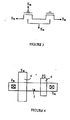
- Fig.3 shows the circuit according to the present invention.
- the device includes two serially connected PMOS transistors, the first PMOS transistor is used as select transistors and the gate of the transistor is connected to the select gate voltage (V SG ).
- the first terminal (source) of the first PMOS transistor is biased to source line voltage, and the second terminal (drain) is connected to the first terminal of the second PMOS transistor and the second terminal of the second PMOS is connected to the bit line voltage (V BL ).
- the gate of the second PMOS transistor acts as the floating gate. It has to be noted that the cell according to the present invention omits the control gate compared to the prior art.
- the channel hot carrier will inject onto the floating gate by applying suitable bias.
- the device includes a doped region 2 (lateral configuration area in the drawing).
- the doped region can be formed by ion implantation, the doped region 2 can be shaped into a stripe structure.
- a first conductive area 4 and a second conductive area 6 are covered on the overlap area to act as selecting transistor gate and floating gate.
- the gate of the selecting transistor comprises a stripe structure and is connected to selecting gate voltage (V SG ).
- V SG selecting gate voltage
- One of the aspects of the present invention is that the control gate is omitted, therefore, the present invention may reduce the device size, meet the requirement of the IC trend and integrate with CMOS process.
- the bit line and contact window of the selecting line can be formed and aligned to the doped region 2 by using lithography and etching process.
- the second conductive area 6 is located at the side of the first conductive area 4 and on the substrate forms cross configuration structure with overlap area to act as floating gate.
- the programming operation is achieved by using channel hot electron injection (CHE) and the floating gate is charged by hot electrons in the programming gate, the voltage level of the floating gate is less than ground level.
- the device cell keeps "turned on”.
- the digital states may be altered by exposing using ultra violate (UV) ray to alter the state. In the erase state, there is no charge in the floating gate.
- UV ultra violate
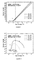
- Fig.9 illustrates the drain current-voltage characteristic and Fig.10 shows the gate current-voltage characteristic.
- the drain bias is negative five or six volts.
- the PMOS gate bias is about negative one volt.
- the carrier will inject onto the floating gate.
- the control gate is omitted.
- the term “automatically inject” refers to that the device does not need to apply bias on the control gate for programming. With reduction of the floating gate bias, the programming mode is then "turned off". The higher I G /I D efficient can be obtained with lower power consumption.
- the conditions for writing a "digital one" and a "digital zero" refer to Table one and Fig.5 and Fig.6.
- the selected word line is grounded and the unselected word line is set in a range of 3-8 volts, preferably about five volts.
- the selected bit line is grounded and the bias of the unselected bit line is set in a range of 3-8 volts, preferably 5 volts, bias applies on the source node and N well is connected to 3-8 volts.
- the PMOS transistor of the selected transistor turns on and the hot channel electron injects onto the floating gate of the second transistor.
- the selected word line is grounded and 3-8 volts is biased to the unselected word line.
- the selected bit line is set to a range of 3-8 volts, preferably 5 volts and the unselected bit line is set to a range of 3-8 volts.
- the source node N well are respectively connected to 3-8 volts. The device is under the state of "off” and therefore the hot carrier is unable to inject into the floating gate.
- the selected word line is grounded.
- the unselected word line is biased to 2.5-5 volts and selected bit line is biased to 3.3 volts.
- the source node is also biased to 2.5-5 volts.
- the N well is respectively connected to 2.5-5 volts.
- the device does not need the control gate for programming.
- the floating gate may self-charge to define the digital status.
- the feature of the present invention includes: the device can be manufactured by standard CMOS processes. The space for forming the control gate can be omitted, thereby reducing the layout area.
- Fig.11 illustrates the cell array.
- the drain in the mode for writing a "digital one" the drain is biased to five or six volts and the gate of select transistor is connected to ground.
- Other cells that are not under programming on the same bit line do not suffer the drain disturbance that typically occurs at stacked gate memory, this is because that the transistor is at an off-state and the electric field between the drain and floating gate is not strong enough to inject/generate hot carrier. Further, the potential coupling of the floating gate is not induced by the word line, thereby eliminating the gate disturbance phenomenon.
Landscapes
- Engineering & Computer Science (AREA)
- Microelectronics & Electronic Packaging (AREA)
- Non-Volatile Memory (AREA)
- Semiconductor Memories (AREA)
- Read Only Memory (AREA)
Abstract
Description
| Operation | Select WL | Unselect WL | Select BL | Unselect BL | Source line | N-well | |
| Write one | 0 | 5 V | 0 | 5 | 5 V | ||
| Write zero | 0 | 5 | 5 | 5V | 5 | 5 V | |
| Read | 0 V | 3.3 V | 3.3 V | 3.3 V | 3.3 V | 3.3 V |
Claims (21)
- An erasable programmable read only memory comprising:two serially connected P-type metal-oxide semiconductor (MOS) transistors, wherein a first P-type metal-oxide semiconductor transistor acts as select transistor, a gate of said first P-type metal-oxide semiconductor transistor is coupled to select gate voltage, a first node of said first P-type metal-oxide semiconductor transistor connected to source line voltage, a second node of said first P-type metal-oxide semiconductor transistor connected to a first node of a second P-type metal-oxide semiconductor transistor, wherein a second node of said second P-type metal-oxide semiconductor transistor is connected to bit line voltage, wherein a gate of said second P-type metal-oxide semiconductor transistor serves as a floating gate, characterized in that said erasable programmable read only memory does not need to bias a certain voltage on a control gate for programming and thereby injecting hot carriers onto said floating gate.
- The erasable programmable read only memory of claim 1 characterized in that during a mode for writing a "digital one", a selected word line is grounded and a unselected word line is biased to about a first voltage, wherein a selected bit line is grounded, an unselected bit line is about said first voltage, a source node and an N well are connected to said first voltage, thereby turning on said selected transistor and injecting hot channel carriers onto said floating gate of said second P-type metal-oxide semiconductor transistor.
- The erasable programmable read only memory of claim 2
characterized in that said first voltage ranges from 3-8 volts. - The erasable programmable read only memory of claim 1 characterized in that during a mode for writing a "digital zero", a selected word line is grounded and an unselected word line is applied to a second voltage, a selected bit line is about said second voltage and an unselected bit line is also about said second voltage, a source node and an N well are respectively connected to said second voltage, thereby turning off said select transistor and hot carrier is unable to inject onto said floating gate.
- The erasable programmable read only memory of claim 4 characterized in that said second voltage ranges from 3-8 volts.
- The erasable programmable read only memory of claim 1 characterized in that during read mode, a selected word line is grounded and an unselected word line is biased to a third voltage, a selected bit line is about a forth voltage, an unselected bit line is biased to said third voltage, a source node is also biased to said third voltage and an N well is connected to said third voltage, thereby turning on said select transistor for reading the status stored in said floating gate.
- The erasable programmable read only memory of claim 6 characterized in that said third voltage ranges from 2.5-5 volts.
- The erasable programmable read only memory of claim 6 characterized in that said fourth voltage ranges from 0-2.5 volts.
- An erasable programmable read only memory that omits a control gate comprising:characterized by:a doped region (2) formed by ion implantation in a substrate;and that a feature of said erasable programmable read only memory is that a control gate is omitted, thereby reducing device size and being integratable with a CMOS process.a first conductive area (4) disposed on said substrate forming a first cross structure with a first overlap area to act as a select transistor gate, and connected to a select gate voltage (VSG); anda second conductive area (6) located at a side of said first conductive region and on said substrate forming a second cross structure with a second overlap area to act as a floating gate;
- The erasable programmable read only memory of claim 9 characterized in that during a mode for writing a "digital one", a selected word line is grounded and an unselected word line is biased to about a first voltage, wherein a selected bit line is grounded, an unselected bit line is about said first voltage, a source node and an N well are connected to said first voltage, thereby turning on said selected transistor and injecting hot channel carrier onto said floating gate of said second P-type metal-oxide semiconductor transistor.
- The erasable programmable read only memory of claim 9 characterized in that during a mode for writing a "digital zero", a selected word line is grounded and an unselected word line is applied to a second voltage, a selected bit line is about said first second voltage and an unselected bit line is also about said second voltage, a source node and an N well are respectively connected to said second voltage, thereby turning off said select transistor and hot carrier is unable to inject onto said floating gate.
- The erasable programmable read only memory of claim 9 characterized in that during a read mode, a selected word line is grounded and an unselected word line is biased to a third voltage, a selected bit line is about a forth voltage, an unselected bit line is biased to said third voltage, a source node is also biased to said third voltage and an N well is connected to said third voltage, thereby turning on said select transistor for reading the status stored in said floating gate.
- The erasable programmable read only memory of claim 9 characterized in that in a cell array, an unselected transistor does not suffer a drain disturbance because said unselected transistor is in an off-state and the electric field between said bit line and said floating gate is not strong enough to inject/generate hot carriers, a coupling of said floating gate is not induced by the word line, thereby eliminating the gate disturbance phenomenon.
- An erasable programmable read only memory comprising:two serially connected P-type metal-oxide semiconductor (MOS) transistors formed on an N-well, wherein a first P-type metal-oxide semiconductor transistor acts as a select transistor, a second P-type metal-oxide semiconductor transistor is connected to said first P-type metal-oxide semiconductor transistor, wherein a gate of said second P-type metal-oxide semiconductor transistor serves as a floating gate, characterized in that in a programming mode, a well voltage is applied to said N-well, a drain of said second P-type metal-oxide semiconductor transistor is biased to a first voltage that is less than said well voltage, thereby coupling a second voltage on said floating gate to turn on a P-channel under said floating gate.
- The erasable programmable read only memory of claim 14 characterized in that a gate of said select transistor is connected to a select gate voltage.
- The erasable programmable read only memory of claim 14 characterized in that a first node of said select transistor is connected to a source line voltage.
- The erasable programmable read only memory of claim 14 characterized in that a second node of said select transistor is connected to a first node of said second P-type metal-oxide semiconductor transistor and a second node of said second P-type metal-oxide semiconductor transistor is connected to a bit line voltage.
- A P-channel single-poly memory unit comprising:characterized by:a P-type metal-oxide-semiconductor (PMOS) select transistor formed on an N-well of a substrate, wherein said PMOS select transistor has a first P-doped source region, a control gate electrode, and a first P-doped drain region, and wherein said first P-doped source region and said first P-doped drain region define a first P-channel under said control gate electrode; anda single-poly PMOS memory cell formed on said N-well, wherein said single-poly PMOS memory cell has a floating gate, a second P-doped drain region and said first P-doped drain region of said PMOS select transistor serves as a second P-doped source region of said single-poly PMOS memory cell, and wherein said second P-doped source region and said second P-doped drain region define a second P-channel under said floating gate.
- The P-channel single-poly memory unit of claim 18 characterized in that there is no control gate located on said floating gate of said single-poly PMOS memory cell.
- The P-channel single-poly memory unit of claim 18 characterized in that during a programming operation a well voltage is applied to said N-well, a first voltage that is less than said well voltage is applied to said second P-doped drain region of said single-poly PMOS memory cell, thereby coupling a second voltage on said floating gate to turn on said second P-channel.
- An erasable programmable read only memory comprising:and by in a program mode, said floating gate acquires an induced floating gate voltage contributed by said bit line voltage, said well voltage, and said source region of said second P-type MOS transistor.an N-well electrically coupled to a well voltage; andtwo serially connected P-type metal-oxide semiconductor (MOS) transistors formed on said N-well, wherein a first P-type MOS transistor comprises:a select gate formed over a channel region of said first P-type MOS transistor and being electrically coupled to a select gate voltage;a first source region being electrically connected to a source line voltage; anda first drain region;
and a second P-type MOS transistor comprises:characterized by:a second source region being electrically connected to said drain region of said first P-type MOS transistor;a second drain region being electrically coupled to a bit line voltage; anda floating gate formed over a floating gate channel defined by said second source region and said second drain region;
Applications Claiming Priority (2)
| Application Number | Priority Date | Filing Date | Title |
|---|---|---|---|
| CNB011368772A CN1192436C (en) | 2001-11-02 | 2001-11-02 | Programming operation method of erasable programmable read-only memory |
| CN01136877 | 2001-11-02 |
Publications (3)
| Publication Number | Publication Date |
|---|---|
| EP1308962A2 true EP1308962A2 (en) | 2003-05-07 |
| EP1308962A3 EP1308962A3 (en) | 2005-09-28 |
| EP1308962B1 EP1308962B1 (en) | 2008-03-05 |
Family
ID=4673975
Family Applications (1)
| Application Number | Title | Priority Date | Filing Date |
|---|---|---|---|
| EP20020024258 Expired - Lifetime EP1308962B1 (en) | 2001-11-02 | 2002-10-31 | Single poly embedded EPROM |
Country Status (3)
| Country | Link |
|---|---|
| EP (1) | EP1308962B1 (en) |
| CN (1) | CN1192436C (en) |
| DE (1) | DE60225401T2 (en) |
Cited By (1)
| Publication number | Priority date | Publication date | Assignee | Title |
|---|---|---|---|---|
| DE112004002678B4 (en) * | 2004-01-29 | 2011-05-05 | Infineon Technologies Ag | Electrically programmable 2-transistor fuse element with simple polysilicon layer and electrically programmable transistor fuse cell |
Families Citing this family (6)
| Publication number | Priority date | Publication date | Assignee | Title |
|---|---|---|---|---|
| US8692310B2 (en) | 2009-02-09 | 2014-04-08 | Spansion Llc | Gate fringing effect based channel formation for semiconductor device |
| CN102024821B (en) * | 2009-09-18 | 2012-08-22 | 中芯国际集成电路制造(上海)有限公司 | Non-volatile memory device as well as non-volatile memory and manufacturing method thereof |
| CN102779552B (en) * | 2011-05-11 | 2015-09-09 | 旺宏电子股份有限公司 | Memory programming method and memory cell programming method in memory array |
| CN102543200A (en) * | 2012-02-10 | 2012-07-04 | 上海宏力半导体制造有限公司 | Reading method of series transistor type one-time programmable memory |
| CN103366821A (en) * | 2013-06-26 | 2013-10-23 | 苏州宽温电子科技有限公司 | Improved differential framework OTP (One Time Programmable) storage unit based on series transistor |
| US10839893B2 (en) * | 2018-09-28 | 2020-11-17 | Kneron (Taiwan) Co., Ltd. | Memory cell with charge trap transistors and method thereof capable of storing data by trapping or detrapping charges |
Family Cites Families (4)
| Publication number | Priority date | Publication date | Assignee | Title |
|---|---|---|---|---|
| US3843954A (en) * | 1972-12-29 | 1974-10-22 | Ibm | High-voltage integrated driver circuit and memory embodying same |
| GB2160049B (en) * | 1984-05-28 | 1987-06-03 | Suwa Seikosha Kk | A non-volatile memory circuit |
| US6118691A (en) * | 1998-04-01 | 2000-09-12 | National Semiconductor Corporation | Memory cell with a Frohmann-Bentchkowsky EPROM memory transistor that reduces the voltage across an unprogrammed memory transistor during a read |
| US6166954A (en) * | 1999-07-14 | 2000-12-26 | Programmable Microelectronics Corporation | Single poly non-volatile memory having a PMOS write path and an NMOS read path |
-
2001
- 2001-11-02 CN CNB011368772A patent/CN1192436C/en not_active Expired - Lifetime
-
2002
- 2002-10-31 EP EP20020024258 patent/EP1308962B1/en not_active Expired - Lifetime
- 2002-10-31 DE DE2002625401 patent/DE60225401T2/en not_active Expired - Lifetime
Cited By (1)
| Publication number | Priority date | Publication date | Assignee | Title |
|---|---|---|---|---|
| DE112004002678B4 (en) * | 2004-01-29 | 2011-05-05 | Infineon Technologies Ag | Electrically programmable 2-transistor fuse element with simple polysilicon layer and electrically programmable transistor fuse cell |
Also Published As
| Publication number | Publication date |
|---|---|
| CN1416174A (en) | 2003-05-07 |
| EP1308962A3 (en) | 2005-09-28 |
| DE60225401D1 (en) | 2008-04-17 |
| EP1308962B1 (en) | 2008-03-05 |
| CN1192436C (en) | 2005-03-09 |
| DE60225401T2 (en) | 2009-03-26 |
Similar Documents
| Publication | Publication Date | Title |
|---|---|---|
| US6678190B2 (en) | Single poly embedded eprom | |
| US7200038B2 (en) | Nonvolatile memory structure | |
| US5687118A (en) | PMOS memory cell with hot electron injection programming and tunnelling erasing | |
| US5301150A (en) | Flash erasable single poly EPROM device | |
| US7209392B2 (en) | Single poly non-volatile memory | |
| US6841821B2 (en) | Non-volatile memory cell fabricated with slight modification to a conventional logic process and methods of operating same | |
| US6457108B1 (en) | Method of operating a system-on-a-chip including entering a standby state in a non-volatile memory while operating the system-on-a-chip from a volatile memory | |
| US6914825B2 (en) | Semiconductor memory device having improved data retention | |
| US6617637B1 (en) | Electrically erasable programmable logic device | |
| US6882574B2 (en) | Single poly UV-erasable programmable read only memory | |
| US7262457B2 (en) | Non-volatile memory cell | |
| US8344440B2 (en) | Three-terminal single poly NMOS non-volatile memory cell with shorter program/erase times | |
| CN117558321B (en) | Nonvolatile semiconductor memory device capable of electrically erasing | |
| EP1408511A1 (en) | Single bit nonvolatile memory cell and methods for programming and erasing thereof | |
| EP1308962B1 (en) | Single poly embedded EPROM | |
| US6163482A (en) | One transistor EEPROM cell using ferro-electric spacer | |
| US7123518B2 (en) | Memory device | |
| JP3954368B2 (en) | Erasable programmable read-only memory | |
| US10008267B2 (en) | Method for operating flash memory | |
| US20110101440A1 (en) | Two pfet soi memory cells | |
| US6711065B2 (en) | 1 T flash memory recovery scheme for over-erasure | |
| US20050179095A1 (en) | Non-volatile memory cell | |
| Dray et al. | A novel memory array based on an annular single-poly EPROM cell for use in standard CMOS technology | |
| KR20020058460A (en) | Nonvolatile memory device |
Legal Events
| Date | Code | Title | Description |
|---|---|---|---|
| PUAI | Public reference made under article 153(3) epc to a published international application that has entered the european phase |
Free format text: ORIGINAL CODE: 0009012 |
|
| 17P | Request for examination filed |
Effective date: 20021031 |
|
| AK | Designated contracting states |
Designated state(s): AT BE BG CH CY CZ DE DK EE ES FI FR GB GR IE IT LI LU MC NL PT SE SK TR |
|
| AX | Request for extension of the european patent |
Extension state: AL LT LV MK RO SI |
|
| PUAL | Search report despatched |
Free format text: ORIGINAL CODE: 0009013 |
|
| AK | Designated contracting states |
Kind code of ref document: A3 Designated state(s): AT BE BG CH CY CZ DE DK EE ES FI FR GB GR IE IT LI LU MC NL PT SE SK TR |
|
| AX | Request for extension of the european patent |
Extension state: AL LT LV MK RO SI |
|
| AKX | Designation fees paid |
Designated state(s): DE FR IT NL |
|
| 17Q | First examination report despatched |
Effective date: 20060119 |
|
| GRAP | Despatch of communication of intention to grant a patent |
Free format text: ORIGINAL CODE: EPIDOSNIGR1 |
|
| RIN1 | Information on inventor provided before grant (corrected) |
Inventor name: SHEN, SHIH-JYE Inventor name: HSU, CHING-HSIANG Inventor name: YANG, CHING-SUNG |
|
| GRAS | Grant fee paid |
Free format text: ORIGINAL CODE: EPIDOSNIGR3 |
|
| GRAA | (expected) grant |
Free format text: ORIGINAL CODE: 0009210 |
|
| AK | Designated contracting states |
Kind code of ref document: B1 Designated state(s): DE FR IT NL |
|
| REF | Corresponds to: |
Ref document number: 60225401 Country of ref document: DE Date of ref document: 20080417 Kind code of ref document: P |
|
| ET | Fr: translation filed | ||
| PLBE | No opposition filed within time limit |
Free format text: ORIGINAL CODE: 0009261 |
|
| STAA | Information on the status of an ep patent application or granted ep patent |
Free format text: STATUS: NO OPPOSITION FILED WITHIN TIME LIMIT |
|
| 26N | No opposition filed |
Effective date: 20081208 |
|
| PG25 | Lapsed in a contracting state [announced via postgrant information from national office to epo] |
Ref country code: IT Free format text: LAPSE BECAUSE OF FAILURE TO SUBMIT A TRANSLATION OF THE DESCRIPTION OR TO PAY THE FEE WITHIN THE PRESCRIBED TIME-LIMIT Effective date: 20080305 |
|
| REG | Reference to a national code |
Ref country code: FR Ref legal event code: PLFP Year of fee payment: 14 |
|
| REG | Reference to a national code |
Ref country code: FR Ref legal event code: PLFP Year of fee payment: 15 |
|
| REG | Reference to a national code |
Ref country code: FR Ref legal event code: PLFP Year of fee payment: 16 |
|
| REG | Reference to a national code |
Ref country code: FR Ref legal event code: PLFP Year of fee payment: 17 |
|
| PGFP | Annual fee paid to national office [announced via postgrant information from national office to epo] |
Ref country code: NL Payment date: 20211008 Year of fee payment: 20 |
|
| PGFP | Annual fee paid to national office [announced via postgrant information from national office to epo] |
Ref country code: DE Payment date: 20211008 Year of fee payment: 20 |
|
| PGFP | Annual fee paid to national office [announced via postgrant information from national office to epo] |
Ref country code: FR Payment date: 20211005 Year of fee payment: 20 |
|
| REG | Reference to a national code |
Ref country code: DE Ref legal event code: R071 Ref document number: 60225401 Country of ref document: DE |
|
| REG | Reference to a national code |
Ref country code: NL Ref legal event code: MK Effective date: 20221030 |