EP1308836A1 - Adder tree structure with reduced carry ripple adder stage - Google Patents
Adder tree structure with reduced carry ripple adder stage Download PDFInfo
- Publication number
- EP1308836A1 EP1308836A1 EP01402820A EP01402820A EP1308836A1 EP 1308836 A1 EP1308836 A1 EP 1308836A1 EP 01402820 A EP01402820 A EP 01402820A EP 01402820 A EP01402820 A EP 01402820A EP 1308836 A1 EP1308836 A1 EP 1308836A1
- Authority
- EP
- European Patent Office
- Prior art keywords
- adder
- vector
- stage
- tree structure
- tree
- Prior art date
- Legal status (The legal status is an assumption and is not a legal conclusion. Google has not performed a legal analysis and makes no representation as to the accuracy of the status listed.)
- Withdrawn
Links
Images



Classifications
-
- G—PHYSICS
- G06—COMPUTING OR CALCULATING; COUNTING
- G06F—ELECTRIC DIGITAL DATA PROCESSING
- G06F7/00—Methods or arrangements for processing data by operating upon the order or content of the data handled
- G06F7/38—Methods or arrangements for performing computations using exclusively denominational number representation, e.g. using binary, ternary, decimal representation
- G06F7/48—Methods or arrangements for performing computations using exclusively denominational number representation, e.g. using binary, ternary, decimal representation using non-contact-making devices, e.g. tube, solid state device; using unspecified devices
- G06F7/50—Adding; Subtracting
- G06F7/505—Adding; Subtracting in bit-parallel fashion, i.e. having a different digit-handling circuit for each denomination
- G06F7/509—Adding; Subtracting in bit-parallel fashion, i.e. having a different digit-handling circuit for each denomination for multiple operands, e.g. digital integrators
Definitions
- This invention relates to adder tree structures commonly used in electronic hardware to sum vectors, and particularly but not exclusively to such structures when used in a multiplier to sum partial products produced in a multiplication process.
- a Wallace tree is a well known implementation of an adder tree designed to sum vectors with a minimum propagation delay. Rather than completely adding the partial products in pairs as known in a ripple adder tree, a Wallace tree sums up all the bits of the same weights in a merged tree.
- full adders are used in Carry-Save-Add (CSA) units, so that 3 equally weighted bits are combined to produce two bits: one bit being the carry, and the other bit being the sum.
- CSA Carry-Save-Add
- Each layer of the tree therefore reduces the number of vectors by a factor of 3:2.
- the tree has as many layers as is necessary to reduce the number of vectors to two of each weight (a carry and a sum).
- a conventional ripple adder is then used to combine these to obtain the final product.
- the delay of such a Wallace tree is proportional to log10(n), where n is the number of partial products combined.
- FIG. 1 The structure of such an arrangement is shown in FIG. 1, where vector inputs 15 are fed to a Wallace tree 10. Two partial vector outputs X1 and X2 of the Wallace tree 10 are then fed to a final stage ripple adder 20, which produces a single output vector X.
- the adder tree structure further comprises a final stage ripple adder, the plurality of adder stages being arranged in a predetermined one of a number of possible configurations, each configuration having an associated final stage ripple adder size, wherein the predetermined configuration is chosen such that the adder tree structure has the smallest final stage ripple adder size of all of the possible configurations.
- the adder tree structure comprises a plurality of adder stages, each adder stage having a plurality of adders, the vector tree position combinations relating to the arrangements of the plurality of adders and the plurality of adder stages.
- the plurality of adder stages preferably include at least one adder stage having an adder arrangement comprising first and second half-adder series, each half-adder series having vector inputs and vector outputs; the vector outputs of the first half-adder series being coupled to the vector inputs of the second half-adder series such that the first and second half-adders are in cascaded arrangement within the at least one adder stage.
- the calculated propagation characteristics refer to the required bit-depth of a final stage adder coupled to the tree structure, the selected vector tree position combination and instantiation being those which lead to a final adder having the smallest bit-depth.
- a known vector adder is shown, using a Wallace tree 10 to sum up n number of IN vectors 15 (IN1[m:11 to INn[m:1n]), where m is the number of bits per vector and 1 is the lowest vector index (the least significant bit of the vector) having a non-zero value in each case.
- the Wallace tree 10 comprises a number of stages, each stage composed of Carry-Save Full- or Half- Adders (FA or HA).
- a FA is shown in FIG.2, and a HA is shown in FIG. 3.
- the Wallace tree structure reduces the summation process into intermediate stages.
- the ratio of input to output vectors will be 3:2 for each stage, leading to a reduction in the number of vectors per stage by 2/3.
- the input vectors are grouped into sets of 3 (for each FA in the stage), and the remaining lines are passed to the next stage (in the case of the penultimate stage (from 4 to 3) one input is by-passed to the final stage.
- the Wallace tree 10 provides two vector outputs X1 and X2. These are fed to a final stage ripple adder 20, which combines X1 and X2 to provide a single vector result X.
- the final stage ripple adder is a Carry-LookAhead stage (CLA) with carry propagation.
- CLA Carry-LookAhead stage
- HA subgroups have two input nodes and two output nodes, and FAs have three input nodes and two output nodes.
- the present invention groups input lines on each stage as follows (where K is the number of inputs for a given stage):
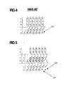
- FIG. 4 there is shown a block 5 representation of the addition of three vectors, A, B and C1 by a FA. Signals coming from the same column (or vector degree) are summed, resulting in a sum in the same column and a carry in the following one, as shown in FIG. 4.
- a double-stage HA structure is shown in which a HA stage is provided using two HAs in 0 a cascaded configuration. This facilitates the 'saving' of 2 bits instead of 1 (bullets 210 and 220).
- This double HA structure has a propagation delay roughly equal to one FA (since HAs are much faster than FAs), and therefore does not introduce a timing problem.
- the invention takes advantage of this HA improved structure which gives a gain of two bit shifts to the left, compared to a FA group (one bit shift) and uses it whenever appropriate. For example, a 10 input stage would not be split in 3 groups of FA and one input bypassing 0 the stage, but by 2 groups of FA and 2 groups of HA. Similarly, when implemented in a DSP multiplier for all-digital filtering, with a 27 input vector adder, 5 bits may be saved in the Final Adder.
- the vector X2 (as shown in FIG. 1) can be written in the following form: (X2 [m], X2[m-1], ..., X2 [s], 0, ..., 0) where s > 0, s being the least significant non-zero bit.
- the final m-bit addition becomes a faster (m-s)-bit addition with the s least significant bits directly output from X1 to the final adder output.
- the Wallace tree structure has a first adder stage 365, a second adder stage 370, a third adder stage 375 and a ripple adder 380.
- This ripple adder 380 is equivalent to the final adder 20 of FIG. 1.
- the first adder stage 365 has two series of FAs (310, 312, 322 being a first series and 320, 322, 324 being a second series) and a series of double-stage HAs 300, 302, 304 as described above with reference to FIG. 4.
- the double-stage HA 300 has a first HA 301 coupled to receive vector inputs to be further described below for providing a sum output s301 and a carry output c301, and a second HA 306 having a first input coupled to receive c301 from the first HA 301, and a second input to be further described below.
- the second HA 306 provides a sum output s306 and a carry output c306.
- the double-stage HA 302 has a first HA 303 which provides a sum output s303 and a carry output c303, and a second HA 307 which provides a sum output s307 and a carry output c307.
- Vector inputs A-H are fed into the first adder stage 365.
- the vector inputs are as follows:
- the ripple adder 380 is a 2 vector adder and is utilised at the 3rd polynomial degree.
- the first HA 301 of the double-stage HA 300 is coupled to receive A0 and B0, and provides s301 and c301.
- the second HA 306 of the double-stage HA 300 is coupled to receive c301 from the first HA 301, and also s3O3, which is the sum output from the first HA 303 of the double-stage HA 302 (representing the carry output of A1 summed with B1).
- Output c301 is then fed into the second HA 306, which leads to the results:
- an algorithm is 0 provided. This takes as its input (box 410) the number of input vectors and their respective least significant non-zero bits. All possible FA and HA instantiations of the tree structure are then computed (box 420).
- the algorithm looks at the least significant non-zero bits of each vector, and maps the vectors on to each instantiation in different position combinations. All possible combinations of vector groupings for all possible instantiations are generated (box 430), and the algorithm calculates the required final adder size for each one (box 440). The combination with the smallest final adder size (that with the highest number of 'saved' bits as illustrated by the bullets in FIGs. 3 and 4) is then selected as the optimum tree structure, and provided as an output (box 450). In other words the algorithm selects the instantiation and grouping combination of vectors which result in a final stage adder in which the number of saved bits is maximised (and the ripple adder depth is minimised).
- the present invention provides a new scheme of grouping input lines on each stage, and introduces a new double-stage structure using a cascaded two-element Half Adder (as illustrated in FIG. 5).
- the present invention improves the overall propagation time in a Wallace tree by reducing the size of the final adder without adding delay to the Wallace tree. This also leads to a reduction in the area of semiconductor material required for the implementation of the Wallace tree structure in an integrated circuit multiplier or DSP, so reducing cost and size.
- each 5 instantiation of a Wallace tree may be overlaid with all possible vector combinations, before the next possible instantiation is computed.
Landscapes
- Physics & Mathematics (AREA)
- General Physics & Mathematics (AREA)
- Engineering & Computer Science (AREA)
- Computational Mathematics (AREA)
- Mathematical Analysis (AREA)
- Pure & Applied Mathematics (AREA)
- Theoretical Computer Science (AREA)
- Computing Systems (AREA)
- Mathematical Optimization (AREA)
- General Engineering & Computer Science (AREA)
- Complex Calculations (AREA)
Abstract
Description
- This invention relates to adder tree structures commonly used in electronic hardware to sum vectors, and particularly but not exclusively to such structures when used in a multiplier to sum partial products produced in a multiplication process.
- In the field of this invention a Wallace tree is a well known implementation of an adder tree designed to sum vectors with a minimum propagation delay. Rather than completely adding the partial products in pairs as known in a ripple adder tree, a Wallace tree sums up all the bits of the same weights in a merged tree. Typically, full adders are used in Carry-Save-Add (CSA) units, so that 3 equally weighted bits are combined to produce two bits: one bit being the carry, and the other bit being the sum. Each layer of the tree therefore reduces the number of vectors by a factor of 3:2. The tree has as many layers as is necessary to reduce the number of vectors to two of each weight (a carry and a sum). A conventional ripple adder is then used to combine these to obtain the final product. The delay of such a Wallace tree is proportional to log10(n), where n is the number of partial products combined. The structure of such an arrangement is shown in FIG. 1, where
vector inputs 15 are fed to aWallace tree 10. Two partial vector outputs X1 and X2 of theWallace tree 10 are then fed to a finalstage ripple adder 20, which produces a single output vector X. - A problem with existing Wallace tree designs is the area of semiconductor material necessary for their implementation.
- From U.S. patent no. 4,839,848 there is known a fast multiplier circuit incorporating parallel arrays of 2-bit and 3-bit adders.
- However, this approach has the disadvantage that the summations required in a multiplier in typical applications such as digital signal processors (DSPs) are timing critical, and are often the cause of shortfall in DSP performance. Indeed the multiplier is often the critical path in DSP architecture and the maximum achievable frequency for the multiplier gives the maximum frequency of the DSP.
- Therefore a trade-off exists between the semiconductor area required, and performance. A need therefore exists for an adder tree structure, DSP, and method wherein the abovementioned disadvantages may be alleviated.
- In accordance with a first aspect of the present invention there is provided an adder tree structure as claimed in claim 1.
- In accordance with a second aspect of the present invention there is provided a Digital Signal Processor as claimed in claim 3.
- In accordance with a third aspect of the present invention there is provided a method as claimed in
claim 4. - In accordance with a fourth aspect of the present invention there is provided a system as claimed in
claim 5. - Preferably the adder tree structure further comprises a final stage ripple adder, the plurality of adder stages being arranged in a predetermined one of a number of possible configurations, each configuration having an associated final stage ripple adder size, wherein the predetermined configuration is chosen such that the adder tree structure has the smallest final stage ripple adder size of all of the possible configurations.
- Preferably the adder tree structure comprises a plurality of adder stages, each adder stage having a plurality of adders, the vector tree position combinations relating to the arrangements of the plurality of adders and the plurality of adder stages.
- The plurality of adder stages preferably include at least one adder stage having an adder arrangement comprising first and second half-adder series, each half-adder series having vector inputs and vector outputs; the vector outputs of the first half-adder series being coupled to the vector inputs of the second half-adder series such that the first and second half-adders are in cascaded arrangement within the at least one adder stage.
- Preferably the calculated propagation characteristics refer to the required bit-depth of a final stage adder coupled to the tree structure, the selected vector tree position combination and instantiation being those which lead to a final adder having the smallest bit-depth.
- In this way an adder tree structure, DSP, system and method are provided which exhibit decreased propagation delay and hence facilitate faster DSP performance while using a reduced amount of semiconductor material for implementation.
- One adder tree structure, DSP, system and method incorporating the present invention will now be described, by way of example only, with reference to the accompanying drawings, in which:
- FIG. 1 shows a block schematic representation of a prior art vector adder, incorporating a Wallace tree;
- FIG. 2 shows a block schematic representation of a Full Adder;
- FIG. 3 shows a block schematic representation of a Half Adder;
- FIG. 4 shows a diagram showing Full Adder operation in a Wallace tree;
- FIG. 5 shows a diagram showing operation of a double stage Half Adder in a Wallace tree in accordance with the present invention;
- FIG. 6 shows an illustrative block diagram of a Wallace tree in accordance with the present invention; and
- FIG. 7 shows a flow diagram illustrating the design process of a Wallace tree in accordance with the present invention.
-
- Referring firstly to FIG. 1, a known vector adder is shown, using a
Wallace tree 10 to sum up n number of IN vectors 15 (IN1[m:11 to INn[m:1n]), where m is the number of bits per vector and 1 is the lowest vector index (the least significant bit of the vector) having a non-zero value in each case. - The
Wallace tree 10 comprises a number of stages, each stage composed of Carry-Save Full- or Half- Adders (FA or HA). A FA is shown in FIG.2, and a HA is shown in FIG. 3. The FA takes three vectors A, B and CI (carry-in), and provides outputs S (Sum) and CO (carry-out). These are calculated as follows: - The HA takes two vectors A and B, and provides outputs S (Sum) and CO (carry-out). These are calculated as follows:
- The Wallace tree structure reduces the summation process into intermediate stages. In a simple arrangement using only FAs, the ratio of input to output vectors will be 3:2 for each stage, leading to a reduction in the number of vectors per stage by 2/3. Also for each stage, the input vectors are grouped into sets of 3 (for each FA in the stage), and the remaining lines are passed to the next stage (in the case of the penultimate stage (from 4 to 3) one input is by-passed to the final stage.
- The
Wallace tree 10 provides two vector outputs X1 and X2. These are fed to a finalstage ripple adder 20, which combines X1 and X2 to provide a single vector result X. - The final stage ripple adder is a Carry-LookAhead stage (CLA) with carry propagation.
- Taking as an example a 14 input Wallace tree, it will be understood that the vector addition is done in 6 stages, carries being propagated from one stage to the other with FAs:
- (i) 14/10 (four FAs with two carried vectors)
- (ii) 10/7 (three FAs with one carried vector)
- (iii) 7/5 (two FAs with one carried vector)
- (iv) 5/4 (one FA with two carried vectors)
- (v) 4/3 (one FA with one carried vector)
- (vi) 3/2 (one FA with no carried vectors)
-
- 5 It is possible to use one or more HA subgroups when the number, modulo 3, of inputs in a stage is not equal to 0. HA subgroups have two input nodes and two output nodes, and FAs have three input nodes and two output nodes.
- The present invention groups input lines on each stage as follows (where K is the number of inputs for a given stage):
- if K modulo 3 equals 0 (in other words if K = 3, 6, 9 5 etc...), all inputs are grouped by means of FAs (each having 3 inputs);
- if K modulo 3 equals 1 (in other words if K = 1, 4, 7 etc...), 2 sets of HAs may be used (e.g., for K = 10, the 0 implementation might be two FAs and two HAs);
- if K modulo 3 equals 2 (in other words if K = 2, 5, 8 etc...), 1 set of HAs may be used (e.g., for K = 8, the implementation might be two FAs and one HA).
- So considering the above example of a 14 input Wallace tree, the vector addition may now be achieved as follows:
- (i) 14/10 (four FAs and one HA)
- (ii) 10/8 (two FAs and two HAs)
- (iii) 8/6 (two FAs and one HA)
- (iv) 6/4 (two FAs)
- (v) 4/3 (one FA with one carried vector)
- (vi) 3/2 (one FA)
-
- Referring first to FIG. 4, there is shown a
block 5 representation of the addition of three vectors, A, B and C1 by a FA. Signals coming from the same column (or vector degree) are summed, resulting in a sum in the same column and a carry in the following one, as shown in FIG. 4. - In this way the meaningful bits of carry output vector CO are shifted one place to the left (illustrated by the bullet 110). The Least Significant Bit (LSB) of this vector is therefore a null bit, and can be ignored in further calculations involving the carry output vector CO.
- Referring now also to FIG. 4, a double-stage HA structure is shown in which a HA stage is provided using two HAs in 0 a cascaded configuration. This facilitates the 'saving' of 2 bits instead of 1 (
bullets 210 and 220). This double HA structure has a propagation delay roughly equal to one FA (since HAs are much faster than FAs), and therefore does not introduce a timing problem. - 5 The invention takes advantage of this HA improved structure which gives a gain of two bit shifts to the left, compared to a FA group (one bit shift) and uses it whenever appropriate. For example, a 10 input stage would not be split in 3 groups of FA and one input bypassing 0 the stage, but by 2 groups of FA and 2 groups of HA. Similarly, when implemented in a DSP multiplier for all-digital filtering, with a 27 input vector adder, 5 bits may be saved in the Final Adder.
- 5 The advantage gained by the above arrangement is dependent on the position of the least significant non-zero bit of each vector. As the vectors propagate through the Wallace tree, the position of the least significant non-zero bits are shifted to the left by varying degrees. Maximum propagation benefit is obtained if vectors that have the same bit-shift are combined. If this is not the case, the advantage of the saved bit is lost, as it cannot be propagated through to the next stage. Therefore the vectors need to be combined in such a way that vectors with 'saved bits' are not combined with vectors without.
- If expressed mathematically, the vector X2 (as shown in FIG. 1) can be written in the following form:
- The final m-bit addition becomes a faster (m-s)-bit addition with the s least significant bits directly output from X1 to the final adder output.
- Moreover this simplification saves some propagate-generate stages, resulting in a saving of semiconductor area also.
- Referring now also to FIG. 6 there is shown an exemplary Wallace tree structure, designed in accordance with the invention. The Wallace tree structure has a
first adder stage 365, asecond adder stage 370, athird adder stage 375 and aripple adder 380. Thisripple adder 380 is equivalent to thefinal adder 20 of FIG. 1. - The
first adder stage 365 has two series of FAs (310, 312, 322 being a first series and 320, 322, 324 being a second series) and a series of double-stage HAs 300, 302, 304 as described above with reference to FIG. 4. - The double-
stage HA 300 has afirst HA 301 coupled to receive vector inputs to be further described below for providing a sum output s301 and a carry output c301, and asecond HA 306 having a first input coupled to receive c301 from thefirst HA 301, and a second input to be further described below. Thesecond HA 306 provides a sum output s306 and a carry output c306. - Similarly the double-
stage HA 302 has afirst HA 303 which provides a sum output s303 and a carry output c303, and asecond HA 307 which provides a sum output s307 and a carry output c307. The same applies for the double-stage HA 304, having HAs 305 and 308, with outputs s305, c305, s308, c308 respectively. - Vector inputs A-H are fed into the
first adder stage 365. The vector inputs are as follows: - XXXXXX
- (1) H
- XXXXXX
- (2) G
- XXXXXX
- (3) F
- XXXXXX
- (4) E
- XXXXXX
- (5) D
- XXXXXX
- (6) C
- XXXXXX
- (7) B
- XXXXXX
- (8) A
- In FIG. 6, only three bits are shown for each vector (A0, A1, A2, etc...) although it will be appreciated that the portion of the Wallace tree not shown in FIG. 6 is substantially similar to that shown. The
ripple adder 380 is a 2 vector adder and is utilised at the 3rd polynomial degree. - In the first stage, the vectors are combined thus:
- A+B (with
HA stages - C+D+E (with
FA stages - F+G+H (with
FA stages -
- The
first HA 301 of the double-stage HA 300 is coupled to receive A0 and B0, and provides s301 and c301. Thesecond HA 306 of the double-stage HA 300 is coupled to receive c301 from thefirst HA 301, and also s3O3, which is the sum output from thefirst HA 303 of the double-stage HA 302 (representing the carry output of A1 summed with B1). - Considering only the bits A0-H0, the partial results from the
HA 301 are: - XXXXXX
- output s301, sum of A0+B0
- XXXXX-
- output c301, carry of A0+B0 (single shift -)
- Output c301 is then fed into the
second HA 306, which leads to the results: - XXXXX-
- output s306, sum of c301+s303 (single shift -)
- XXXX--
- output c306, carry of c301+s303 5 (double shift --)
- The outputs of the two series of FAs are as follows (again only referring to bits A0-H0) :
- XXXXXX
- output s of 310, sum of C0+D0+E0
- XXXXX-
- output c of 310, carry of C0+D0+E0 (shift -)
- XXXXXX
- output s of 320, sum of F0+G0+H0
- XXXXX-
- output c of 320, carry of F0+G0+H0 (shift -)
- It will be understood that the above vector results are truncated, only the rightmost(least significant) bits are shown.
- At the second stage:
- XXXXXX
- output s of 330, sum of (s301)+(s310)+(s320)
- XXXXX-
- output c of 330, carry of (s301)+(s310)+(s320)
- XXXXX-
- output s of 340, sum of (nu11)+(c310)+(c320)
- XXXX--
- output c of 340, carry of (nu11)+(c310)+(c320)
- At this point, it can be seen that the rightmost X on the output of s of 330 has no equivalent (same degree) on any of the other lines. Therefore this bit bypasses the next stage.
- At the third stage:
- XXXXXX
- output s of 350, sum of (s332+s340+c330)
- XXXX--
- output c of 350, carry of (s332+s340+c330)
- XXXX--
- bypass line, output c of 340
- Therefore, at the last stage:
- XXXXXX
- output s of 360, sum of (c340+c350+s352)
- XXX---
- output c of 360, carry of (c340+c350+s352)
- In this way two bits were bypassed, and the HA stages start at degree 3. For the final stage of adders therefore, 3 bits are already resolved.
- Referring now also to FIG. 7, in order to arrive at the optimum structure for a Wallace tree using the mixed HA and FA arrangement described above, an algorithm is 0 provided. This takes as its input (box 410) the number of input vectors and their respective least significant non-zero bits. All possible FA and HA instantiations of the tree structure are then computed (box 420).
- The algorithm looks at the least significant non-zero bits of each vector, and maps the vectors on to each instantiation in different position combinations. All possible combinations of vector groupings for all possible instantiations are generated (box 430), and the algorithm calculates the required final adder size for each one (box 440). The combination with the smallest final adder size (that with the highest number of 'saved' bits as illustrated by the bullets in FIGs. 3 and 4) is then selected as the optimum tree structure, and provided as an output (box 450). In other words the algorithm selects the instantiation and grouping combination of vectors which result in a final stage adder in which the number of saved bits is maximised (and the ripple adder depth is minimised).
- It will be understood that the present invention provides a new scheme of grouping input lines on each stage, and introduces a new double-stage structure using a cascaded two-element Half Adder (as illustrated in FIG. 5).
- In this way the present invention improves the overall propagation time in a Wallace tree by reducing the size of the final adder without adding delay to the Wallace tree. This also leads to a reduction in the area of semiconductor material required for the implementation of the Wallace tree structure in an integrated circuit multiplier or DSP, so reducing cost and size.
- It will be appreciated that the method described above for designing an adder tree structure for summing a number of vectors may be carried out in software running on a processor (not shown), and that the software may be provided as a computer program element carried on any suitable data carrier (also not shown) such as a magnetic or optical computer disc.
- It will be appreciated that alternate embodiments to that described above are possible. For example, the precise methodology and arrangement of the algorithm may differ from that described above. For example rather than computing all possible instantiations first, each 5 instantiation of a Wallace tree may be overlaid with all possible vector combinations, before the next possible instantiation is computed.
- Furthermore it will be appreciated that the above Wallace tree structures are examples only, and the scope of the invention is not limited to these examples.
Claims (9)
- An adder tree structure comprising a plurality of adder stages (365, 370, 375), each adder stage being arranged to sum a plurality of vector inputs to provide partial vector products, at least one of the adder stages (365) including an adder arrangement (300, 302, 304) comprising first (301, 303, 305) and second (306, 307, 308) half-adder series, each half-adder series having vector inputs and vector outputs; the vector outputs of the first half-adder series (301, 303, 305) being coupled to the vector inputs of the second half-adder series (306, 307, 308) such that the first and second half-adders are in cascaded arrangement within the at least one stage (365).
- The adder tree structure of claim 1 further comprising a final stage ripple adder (380), the plurality of adder stages being arranged in a predetermined one of a number of possible configurations, each configuration having an associated final stage ripple adder size,
wherein the predetermined configuration is chosen such that the adder tree structure has the smallest final stage ripple adder size of all of the possible configurations. - A Digital Signal Processor incorporating the adder tree structure of claim 2 or claim 3.
- A method for designing an adder tree structure for summing a number of vectors, the method comprising the steps of:computing (420) a set of instantiations of the adder tree structure for the number of vectors;determining (430) a number of vector tree position combinations for each of the set of instantiations; calculating (440) propagation characteristics for each vector tree position combination of each instantiation; andselecting (450) one of the vector tree position combinations in conjunction with one of the set of instantiations in dependence upon the propagation characteristics.
- A system for designing an adder tree structure for summing a number of vectors, the system comprising:means (420) for computing a set of instantiations of the adder tree structure for the number of vectors;means (430) for determining a number of vector tree position combinations for each of the set of instantiations;means (440) for calculating propagation characteristics for each vector tree position combination of each instantiation; andmeans (450) for selecting one of the vector tree position combinations in conjunction with one of the set of instantiations in dependence upon the propagation characteristics.
- The method of claim 4 or system of claim 5, wherein the adder tree structure comprises a plurality of adder stages (365, 370, 375), each adder stage having a plurality of adders (300, 310, 320), the vector tree position combinations relating to the arrangements of the plurality of adders (300, 310, 320) and the plurality of adder stages(365, 370, 375).
- The method or system of claim 6 wherein the plurality of adder stages (365, 370, 375) include at least one adder stage (365) having an adder arrangement (300) comprising first (301, 303, 305) and second (306, 307, 308) half-adder series, each half-adder series having vector inputs and vector outputs; the vector outputs of the first half-adder series (301, 303, 305) being coupled to the vector inputs of the second half-adder series (306, 307, 308) such that the first and second half-adders are in cascaded arrangement within the at least one adder stage (365).
- The method or system of any one of claims 4 to 7, wherein the calculated propagation characteristics refer to the required bit-depth of a final stage adder (380) coupled to the tree structure, the selected vector tree position combination and instantiation being those which lead to a final adder (380) having the smallest bit-depth.
- A computer program element comprising computer program means for performing the method of claim 4 or any one of claims 5 to 8 when dependent from claim 4.
Priority Applications (2)
| Application Number | Priority Date | Filing Date | Title |
|---|---|---|---|
| EP01402820A EP1308836A1 (en) | 2001-10-31 | 2001-10-31 | Adder tree structure with reduced carry ripple adder stage |
| US10/282,523 US7124162B2 (en) | 2001-10-31 | 2002-10-29 | Adder tree structure digital signal processor system and method |
Applications Claiming Priority (1)
| Application Number | Priority Date | Filing Date | Title |
|---|---|---|---|
| EP01402820A EP1308836A1 (en) | 2001-10-31 | 2001-10-31 | Adder tree structure with reduced carry ripple adder stage |
Publications (1)
| Publication Number | Publication Date |
|---|---|
| EP1308836A1 true EP1308836A1 (en) | 2003-05-07 |
Family
ID=8182948
Family Applications (1)
| Application Number | Title | Priority Date | Filing Date |
|---|---|---|---|
| EP01402820A Withdrawn EP1308836A1 (en) | 2001-10-31 | 2001-10-31 | Adder tree structure with reduced carry ripple adder stage |
Country Status (2)
| Country | Link |
|---|---|
| US (1) | US7124162B2 (en) |
| EP (1) | EP1308836A1 (en) |
Cited By (2)
| Publication number | Priority date | Publication date | Assignee | Title |
|---|---|---|---|---|
| CN108345658A (en) * | 2018-01-30 | 2018-07-31 | 中国平安人寿保险股份有限公司 | Algorithm calculates decomposing process, server and the storage medium of track |
| CN114564170A (en) * | 2021-02-11 | 2022-05-31 | 台湾积体电路制造股份有限公司 | Adder tree circuit, adder circuit and method for operating full adder |
Families Citing this family (4)
| Publication number | Priority date | Publication date | Assignee | Title |
|---|---|---|---|---|
| US7447726B2 (en) * | 2004-06-03 | 2008-11-04 | Arm Limited | Polynomial and integer multiplication |
| US20060004903A1 (en) * | 2004-06-30 | 2006-01-05 | Itay Admon | CSA tree constellation |
| WO2010045378A2 (en) * | 2008-10-14 | 2010-04-22 | The Research Foundation Of State University Of New York (Sunyrf) | Generating partial sums |
| CN115220689B (en) * | 2022-07-29 | 2026-06-26 | 中国电子科技集团公司第十四研究所 | A hierarchical addition tree structure module with fine-grained, accurate, and reconfigurable approximate computation. |
Citations (6)
| Publication number | Priority date | Publication date | Assignee | Title |
|---|---|---|---|---|
| US4463439A (en) * | 1982-05-17 | 1984-07-31 | International Business Machines Corporation | Sum and carry outputs with shared subfunctions |
| US5473558A (en) * | 1993-01-22 | 1995-12-05 | Sony Corporation | Method for generating hardware description of multiplier and/or multiplier-adder |
| US5798956A (en) * | 1994-09-10 | 1998-08-25 | Lg Semicon Co., Ltd. | Parallel multiplier |
| EP0862110A2 (en) * | 1997-02-28 | 1998-09-02 | Digital Equipment Corporation | Wallace-tree multipliers using half and full adders |
| US5912832A (en) * | 1996-09-12 | 1999-06-15 | Board Of Regents, The University Of Texas System | Fast n-bit by n-bit multipliers using 4-bit by 4-bit multipliers and cascaded adders |
| US6029187A (en) * | 1997-10-28 | 2000-02-22 | Atmel Corporation | Fast regular multiplier architecture |
Family Cites Families (5)
| Publication number | Priority date | Publication date | Assignee | Title |
|---|---|---|---|---|
| US4868778A (en) * | 1987-05-19 | 1989-09-19 | Harris Corporation | Speed enhancement for multipliers using minimal path algorithm |
| US4839848A (en) * | 1987-09-14 | 1989-06-13 | Unisys Corporation | Fast multiplier circuit incorporating parallel arrays of two-bit and three-bit adders |
| KR100359965B1 (en) * | 1995-04-11 | 2003-03-15 | 캐논 가부시끼가이샤 | Processor, its operation method, and data processor |
| US6687722B1 (en) * | 2000-03-16 | 2004-02-03 | Agere Systems, Inc. | High-speed/low power finite impulse response filter |
| US7213043B2 (en) * | 2003-01-21 | 2007-05-01 | Lsi Logic Corporation | Sparce-redundant fixed point arithmetic modules |
-
2001
- 2001-10-31 EP EP01402820A patent/EP1308836A1/en not_active Withdrawn
-
2002
- 2002-10-29 US US10/282,523 patent/US7124162B2/en not_active Expired - Lifetime
Patent Citations (6)
| Publication number | Priority date | Publication date | Assignee | Title |
|---|---|---|---|---|
| US4463439A (en) * | 1982-05-17 | 1984-07-31 | International Business Machines Corporation | Sum and carry outputs with shared subfunctions |
| US5473558A (en) * | 1993-01-22 | 1995-12-05 | Sony Corporation | Method for generating hardware description of multiplier and/or multiplier-adder |
| US5798956A (en) * | 1994-09-10 | 1998-08-25 | Lg Semicon Co., Ltd. | Parallel multiplier |
| US5912832A (en) * | 1996-09-12 | 1999-06-15 | Board Of Regents, The University Of Texas System | Fast n-bit by n-bit multipliers using 4-bit by 4-bit multipliers and cascaded adders |
| EP0862110A2 (en) * | 1997-02-28 | 1998-09-02 | Digital Equipment Corporation | Wallace-tree multipliers using half and full adders |
| US6029187A (en) * | 1997-10-28 | 2000-02-22 | Atmel Corporation | Fast regular multiplier architecture |
Non-Patent Citations (2)
| Title |
|---|
| PALACIOS-PAWLOVSKY A: "A NEW ALGORITHM FOR THE CONFIGURATION OF FAST ADDER TREES", IEICE TRANSACTIONS ON FUNDAMENTALS OF ELECTRONICS, COMMUNICATIONS AND COMPUTER SCIENCES, INSTITUTE OF ELECTRONICS INFORMATION AND COMM. ENG. TOKYO, JP, vol. E83-A, no. 12, December 2000 (2000-12-01), pages 2426 - 2430, XP001036392, ISSN: 0916-8508 * |
| ZHONGDE WANG ET AL: "A NEW DESIGN TECHNIQUE FOR COLUMN COMPRESSION MULTIPLIERS", IEEE TRANSACTIONS ON COMPUTERS, IEEE INC. NEW YORK, US, vol. 44, no. 8, 1 August 1995 (1995-08-01), pages 962 - 970, XP000525954, ISSN: 0018-9340 * |
Cited By (5)
| Publication number | Priority date | Publication date | Assignee | Title |
|---|---|---|---|---|
| CN108345658A (en) * | 2018-01-30 | 2018-07-31 | 中国平安人寿保险股份有限公司 | Algorithm calculates decomposing process, server and the storage medium of track |
| CN108345658B (en) * | 2018-01-30 | 2020-12-01 | 中国平安人寿保险股份有限公司 | Decomposition processing method of algorithm calculation track, server and storage medium |
| CN114564170A (en) * | 2021-02-11 | 2022-05-31 | 台湾积体电路制造股份有限公司 | Adder tree circuit, adder circuit and method for operating full adder |
| TWI788220B (en) * | 2021-02-11 | 2022-12-21 | 台灣積體電路製造股份有限公司 | Adder tree circuit and adder circuit and operating method thereof |
| US12399684B2 (en) | 2021-02-11 | 2025-08-26 | Taiwan Semiconductor Manufacturing Company, Ltd. | Low power adder tree structure |
Also Published As
| Publication number | Publication date |
|---|---|
| US20030093454A1 (en) | 2003-05-15 |
| US7124162B2 (en) | 2006-10-17 |
Similar Documents
| Publication | Publication Date | Title |
|---|---|---|
| Fritz et al. | Fast binary counters based on symmetric stacking | |
| EP0448367B1 (en) | High speed digital parallel multiplier | |
| US7313585B2 (en) | Multiplier circuit | |
| US7395304B2 (en) | Method and apparatus for performing single-cycle addition or subtraction and comparison in redundant form arithmetic | |
| EP0613082B1 (en) | 4:2 adder and multiplier circuit employing the same | |
| WO1993022721A1 (en) | Compact multiplier | |
| EP0811908B1 (en) | Two's complement multiplier | |
| US6018758A (en) | Squarer with diagonal row merged into folded partial product array | |
| US6065033A (en) | Wallace-tree multipliers using half and full adders | |
| US5862068A (en) | Arithmetic circuit for calculating a square-root of a sum of squares | |
| US7124162B2 (en) | Adder tree structure digital signal processor system and method | |
| EP1052568B1 (en) | Three input split-adder | |
| US7139789B2 (en) | Adder increment circuit | |
| US7461107B2 (en) | Converter circuit for converting 1-redundant representation of an integer | |
| CN120435705A (en) | Chip, method and device for modular multiplication | |
| JPH03228121A (en) | Priority encoder | |
| US7003538B2 (en) | Process and apparatus for finite field multiplication (FFM) | |
| EP1710689A1 (en) | Combining circuitry for multipliers | |
| Jaberipur et al. | A Parallel Prefix Modulo-(2 q+ 2 q− 1+ 1) Adder via Diminished-1 Representation of Residues | |
| US7277909B2 (en) | High speed adder | |
| US20040267862A1 (en) | Adder including generate and propagate bits corresponding to multiple columns | |
| US5944777A (en) | Method and apparatus for generating carries in an adder circuit | |
| US20080025296A1 (en) | Conditional Selection Adder and Method of Conditional Selection Adding | |
| EP4726530A1 (en) | Digital four-bit combinational multiplier circuit | |
| US20250245007A1 (en) | Hardware acceleration for pipelined floating point operations |
Legal Events
| Date | Code | Title | Description |
|---|---|---|---|
| PUAI | Public reference made under article 153(3) epc to a published international application that has entered the european phase |
Free format text: ORIGINAL CODE: 0009012 |
|
| AK | Designated contracting states |
Designated state(s): AT BE CH CY DE DK ES FI FR GB GR IE IT LI LU MC NL PT SE TR |
|
| AX | Request for extension of the european patent |
Extension state: AL LT LV MK RO SI |
|
| 17P | Request for examination filed |
Effective date: 20031107 |
|
| AKX | Designation fees paid |
Designated state(s): AT BE CH CY DE DK ES FI FR GB GR IE IT LI LU MC NL PT SE TR |
|
| RAP1 | Party data changed (applicant data changed or rights of an application transferred) |
Owner name: FREESCALE SEMICONDUCTOR, INC. |
|
| 17Q | First examination report despatched |
Effective date: 20060330 |
|
| STAA | Information on the status of an ep patent application or granted ep patent |
Free format text: STATUS: THE APPLICATION IS DEEMED TO BE WITHDRAWN |
|
| 18D | Application deemed to be withdrawn |
Effective date: 20070811 |