EP1308824A2 - Wireless communication device and corresponding portable computer - Google Patents
Wireless communication device and corresponding portable computer Download PDFInfo
- Publication number
- EP1308824A2 EP1308824A2 EP02019445A EP02019445A EP1308824A2 EP 1308824 A2 EP1308824 A2 EP 1308824A2 EP 02019445 A EP02019445 A EP 02019445A EP 02019445 A EP02019445 A EP 02019445A EP 1308824 A2 EP1308824 A2 EP 1308824A2
- Authority
- EP
- European Patent Office
- Prior art keywords
- wireless communication
- communication device
- processing apparatus
- circuit board
- printed circuit
- Prior art date
- Legal status (The legal status is an assumption and is not a legal conclusion. Google has not performed a legal analysis and makes no representation as to the accuracy of the status listed.)
- Withdrawn
Links
Images


Classifications
-
- H—ELECTRICITY
- H01—ELECTRIC ELEMENTS
- H01Q—ANTENNAS, i.e. RADIO AERIALS
- H01Q1/00—Details of, or arrangements associated with, antennas
- H01Q1/12—Supports; Mounting means
- H01Q1/22—Supports; Mounting means by structural association with other equipment or articles
- H01Q1/24—Supports; Mounting means by structural association with other equipment or articles with receiving set
-
- H—ELECTRICITY
- H01—ELECTRIC ELEMENTS
- H01Q—ANTENNAS, i.e. RADIO AERIALS
- H01Q9/00—Electrically-short antennas having dimensions not more than twice the operating wavelength and consisting of conductive active radiating elements
- H01Q9/04—Resonant antennas
- H01Q9/0407—Substantially flat resonant element parallel to ground plane, e.g. patch antenna
-
- G—PHYSICS
- G06—COMPUTING OR CALCULATING; COUNTING
- G06F—ELECTRIC DIGITAL DATA PROCESSING
- G06F1/00—Details not covered by groups G06F3/00 - G06F13/00 and G06F21/00
- G06F1/16—Constructional details or arrangements
- G06F1/1613—Constructional details or arrangements for portable computers
- G06F1/1615—Constructional details or arrangements for portable computers with several enclosures having relative motions, each enclosure supporting at least one I/O or computing function
- G06F1/1616—Constructional details or arrangements for portable computers with several enclosures having relative motions, each enclosure supporting at least one I/O or computing function with folding flat displays, e.g. laptop computers or notebooks having a clamshell configuration, with body parts pivoting to an open position around an axis parallel to the plane they define in closed position
-
- G—PHYSICS
- G06—COMPUTING OR CALCULATING; COUNTING
- G06F—ELECTRIC DIGITAL DATA PROCESSING
- G06F1/00—Details not covered by groups G06F3/00 - G06F13/00 and G06F21/00
- G06F1/16—Constructional details or arrangements
- G06F1/1613—Constructional details or arrangements for portable computers
- G06F1/1632—External expansion units, e.g. docking stations
-
- G—PHYSICS
- G06—COMPUTING OR CALCULATING; COUNTING
- G06F—ELECTRIC DIGITAL DATA PROCESSING
- G06F1/00—Details not covered by groups G06F3/00 - G06F13/00 and G06F21/00
- G06F1/16—Constructional details or arrangements
- G06F1/1613—Constructional details or arrangements for portable computers
- G06F1/1633—Constructional details or arrangements of portable computers not specific to the type of enclosures covered by groups G06F1/1615 - G06F1/1626
- G06F1/1637—Details related to the display arrangement, including those related to the mounting of the display in the housing
-
- H—ELECTRICITY
- H01—ELECTRIC ELEMENTS
- H01Q—ANTENNAS, i.e. RADIO AERIALS
- H01Q1/00—Details of, or arrangements associated with, antennas
- H01Q1/08—Means for collapsing antennas or parts thereof
- H01Q1/088—Quick-releasable antenna elements
-
- H—ELECTRICITY
- H01—ELECTRIC ELEMENTS
- H01Q—ANTENNAS, i.e. RADIO AERIALS
- H01Q1/00—Details of, or arrangements associated with, antennas
- H01Q1/12—Supports; Mounting means
- H01Q1/22—Supports; Mounting means by structural association with other equipment or articles
- H01Q1/2258—Supports; Mounting means by structural association with other equipment or articles used with computer equipment
-
- H—ELECTRICITY
- H01—ELECTRIC ELEMENTS
- H01Q—ANTENNAS, i.e. RADIO AERIALS
- H01Q23/00—Antennas with active circuits or circuit elements integrated within them or attached to them
Definitions
- the present invention relates to a wireless communication device and an information-processing apparatus that can hold the device.
- wireless communication devices have come to be mounted in mobile information-processing apparatuses such as notebook-type personal computer and PDAs.
- a first method is to incorporate the wireless communication device into the housing of the information-processing apparatus.
- the second method is to insert the device in the form of a PC card into a PC card slot provided in the housing of the information-processing apparatus.
- the second method is preferable in view of the manufacturing cost of the mobile information-processing apparatus. This is because the PC card (i.e., wireless communication device) is an optional unit, which the user buys and inserts into the PC card slot after he or she has bought the mobile information-processing apparatus.
- Jpn. Pat. Appln. KOKAI Publication No. 10-283449 discloses a wireless communication card shaped like a PC card.
- the wireless communication card is an extended-type PC card. While inserted in the PC card slot of a mobile information-processing apparatus, the card has its extended part protruding from the housing of the apparatus. The antenna of the wireless communication card is incorporated in the extended part in order to enhance the wireless communication efficiency.
- An antenna is mounted on a dielectric card.
- the antenna card may be hingeable or slideably mounted to a mobile computer.
- the antenna card is storable in a recess in the display portion of the mobile computer when not in use. When in use, the antenna card is either rotatably or slideably extended to a deployed position away from the display portion of the mobile computer.
- the extended part which protrudes from the housing of the apparatus, is not resistant to mechanical impacts.
- the extended section may be greatly damaged by an impact, depending on the direction of the impact. It may be broken if the user accidentally drops it onto the floor or hits it against anything hard. If this should happen, not only the housing of the extended part, but also the antenna and electronic components that are provided in this part may be broken.
- Embodiments of the present invention provide a wireless communication device that can reliably perform its function while held in a host apparatus, without having its antenna protruding from the housing of the apparatus.
- a planar antenna to be removably held in a surface of a host apparatus having a wireless communication function.
- the planar antenna comprises an electromagnetic radiation surface that is substantially flush with a surface of the host apparatus during wireless communication.
- a wireless communication device removably held in a host apparatus.
- the wireless communication device comprises a planar antenna module having an electromagnetic radiation surface substantially flush with a surface of the host apparatus during operation of the wireless communication device.
- the surface of the host apparatus is an outer surface such that the electromagnetic radiation surface is substantially flush with the outer surface during operation of the wireless communication device.
- the wireless communication device comprises a printed circuit board including electronic components configured to perform wireless communication.
- a cover is provided for covering the printed circuit board and the electronic components.
- the planar antenna module may be provided in an upper surface of the cover such that when the wireless communication device is held in the host apparatus the upper surface of the cover and the electromagnetic radiation surface are substantially flush with the surface of the host apparatus.
- the upper surface of the cover has a recess, and the planar antenna module is embedded in the recess and the cover has an inner surface covered with a metal layer.
- a connector is provided on a lower surface of the printed circuit board and is configured to connect the printed circuit board to the host apparatus.
- a power source is removably mounted on a lower surface of the printed circuit board for supplying electric power to the electronic components.
- the power source is a battery.
- the power source is one or more solar cells.
- the power source may be a combination of at least one battery and one or more solar cells.
- the host apparatus is an information-processing apparatus for performing wireless communication.
- the information-processing apparatus comprises a housing, a display unit rotatable, with respect to the housing, between an opened position and a closed position, and having a front surface and a back surface, the back surface having a recess therein.
- the wireless communication device is removably provided in the recess and includes a planar antenna module having an electromagnetic radiation surface substantially flush with the back surface of the information-processing apparatus during operation of the wireless communication device.
- the information-processing apparatus is, for example, a mobile apparatus such as, but not limited to, a notebook-type personal computer or a PDA.
- the apparatus will be described as a notebook-type personal computer 1.
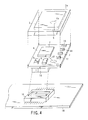
- FIG. 1 shows the notebook-type personal computer 1 as viewed from the rear and having its display unit opened.
- the computer 1 comprises a housing 101 and a display unit 102.
- the display unit 102 incorporates a flat panel display that is an LCD (Liquid Crystal Display).
- the display unit 102 is hinged to the housing 102 and can be rotated, with respect to the housing 101, between an opened position and a closed position.
- the housing 101 is shaped like a shallow rectangular box. Input devices, such as a keyboard and a pointing device, are arranged on the upper surface of the housing 101.
- a display hinge 104 is secured to the rear edge of the upper surface of the housing 101. The display hinge 104 supports the display unit 102 to the housing 102, allowing the display unit 102 to rotate between the opened position and the closed position.
- the display unit 102 has a recess 103 in its back.
- the recess 103 can accommodate a wireless communication device 2.
- a printed circuit board (not shown) lies on the bottom of the recess 103 to connect the wireless communication device 2 to the personal computer 1.
- the wireless communication device 2 is a module that comprises a housing, some electronic components and an antenna.
- the electronic components and the antenna cooperate to perform wireless communication.
- the housing of the wireless communication device 2 has such shape and size as can be fitted in the recess 103 made in the back of the display unit 102 of the personal computer 1. Since the recess 103 defines a substantially rectangular space, the housing of the wireless communication device 2 is a rectangular box that is almost as large as (i.e., a little smaller than) the recess 103.
- the wireless communication device 2 has a planer antenna module 3, which is embedded in the upper surface of the housing.
- the planer antenna module 3 has an electromagnetic radiation surface. The radiation surface is exposed outside and substantially flush with the upper surface of the housing of the wireless communication device 2.
- the planar antenna module 3 has a relatively high directivity.
- the region that the module 3 can cover to receive radio waves tends to lie in the front of the electromagnetic radiation surface (i.e., at the back of the display unit 102), rather than at the back of the radiation surface (i.e., in front of the display unit 102). Nonetheless, the planar antenna module 3 can also cover a region lying at the back of the radiation surface. This is because the recess 103 made in the back of the display unit 102 is located near the upper edge thereof.
- FIG. 2 shows the personal computer 1 that holds the wireless communication device 2.
- the wireless communication device 2 is fitted in the recess 103 cut in the back of the display unit 102. While held in the recess 103, the upper surface of the wireless communication device 2 is substantially flush with the back of the display unit 102 and does not project from the display unit 102. Hence, the back of the display unit 102 is flat and smooth as a whole. Since its electromagnetic radiation surface is exposed in its entirety, the planer antenna module 3 can advantageously achieve efficient radio communication, though its antenna section does not protrude from the display unit 102 of the personal computer 1.
- the wireless communication device 2 is an optional one that can be inserted and removed into and from the recess 103.
- the recess 103 may be filled with a cap made of, for example, rubber, while the device 2 is not being used in combination with the personal computer 1. If this is the case, the back of the display unit 102 can be flat and smooth as a whole.
- FIG. 3 is a cross-sectional view of the display unit 102, showing the recess 103 and some components of the unit 102, which lie near the recess 103.
- the display unit 102 comprises an outer wall 102a that defines the back of the unit 102.
- the outer wall 102a has a rectangular opening, through which the wireless communication device 2 can be inserted into the recess 103.
- the display unit 102 contains a flat panel display 106.
- the flat panel display 106 is arranged, with its back opposing the back of the display unit 102.
- a metal plate 105 covers the entire back of the flat panel display 106.
- the metal plate 105 serves as the frame of the flat panel display 106.
- the printed circuit board 18, mentioned earlier, lies between the outer wall 102a and the metal plate 105.
- the printed circuit board 18 has a connector 16 that can connect the wireless communication device 2 to the personal computer 1.
- the space between the printed circuit board 18 and the wall 102a, which opens at the wall 102, is the recess 103.
- the wireless communication device 2 has a connector 10 on the lower surface.
- the connector 10 contacts the connector 16 provided in the flat panel display unit 106, as long as the wireless communication device 2 remains in the recess 103.
- the wireless communication device 2 is thus connected to the personal computer 1, mechanically and electrically.
- the metal plate 105 can shield electromagnetic waves. It can therefore minimize the influence that the electromagnetic waves emanating from the wireless communication device 2 may impose on the electronic components of the computer 1.
- the wireless communication device 2 will now be described in terms of its structure.
- FIG. 4 is an exploded view of the wireless communication device 2.
- the wireless communication device 2 includes a cover 2a and a printed circuit board 6.
- the cover 2a covers the printed circuit board 6.
- the cover 2a is a rectangular case that opens at the lower surface.
- the planer antenna module 3 is embedded in the upper surface of the cover 2a, with its electromagnetic radiation surface exposed to the outside of the computer 1.
- the planer antenna module 3 has an insulating base that is a thin plate that may be about 4 mm thick. One surface of the insulating base functions as the electromagnetic radiation surface.
- the planar antenna module 3 is, for example, a patch antenna that is one type of a microstrip antenna.
- a contact 4a lies on the electromagnetic radiation surface of the planar antenna module 3.
- the contact 4a connects the radiation surface to a conduction path that penetrates the insulating base. More precisely, the contact 4a is connected to the feeding terminal 5 provided on the back of the planar antenna module 3.
- the feeding terminal 5 extends from the lower surface of the cover 2a and is connected to the antenna terminal 11 mounted on the printed circuit board 6 via a wiring cable (not shown).
- a land or connector 17 that is provided on the printed circuit board 6 connects the antenna terminal 11 to the wiring cable.
- the printed circuit board 6 is a hard plate. It holds a wireless communication IC 7 on its surface.
- a quartz oscillator 8, a flash EEPROM 9, and other electronic components 12 to 15 are also mounted on the printed circuit board 6.
- the electronic components 12 to 15 are, for example, chip resistors and chip capacitors.
- the wireless communication IC 7 is the main electronic component provided on the printed circuit board 6 and is designed to implement wireless communication.
- the IC 7 is a one-chip LSI comprising an RF section and a base-band section.
- the RF section performs upward conversion, converting an intermediate frequency to an RF frequency.
- the RF section also performs downward conversion, from an RF frequency to an intermediate frequency.
- the base-band section modulates data to transmit and demodulates data received, in accordance with a prescribed protocol of wireless communication.
- the quartz oscillator 8 generates the operating clock signal of the wireless communication IC 7.
- the flash EEPROM 9 stores the firmware that controls the wireless communication IC 7.
- the firmware is a program that describes the sequence of protocol stacks for controlling the operation of the base-band section.
- the printed circuit board 6 serves as the base of the wireless communication device 2.
- the printed circuit board 6 holds a connector 10 (i.e., plug) on its lower surface.
- the connector 10 can be connected to the connector 16, or receptacle (e.g., stacking connector), mounted on a printed circuit board 18.
- the printed circuit board 18 is provided in the back of the display unit 102 of the personal computer 1.
- FIG. 5 is a cross-sectional view of the wireless communication device 2.
- the cover 2a covers the upper surface of the printed circuit board 6 and, hence, all electronic components mounted on the upper surface of the printed circuit board 6.
- the planar antenna module 3 is embedded in the upper surface of the cover 2a, with its electromagnetic radiation surface lying substantially flush with the upper surface of the cover 2a.
- the cover 2a has a recess in its upper surface and the planar antenna module 3 is held in the recess.
- the module 3 comprises a base 301 and a metal layer 302.
- the base 301 is made of insulating material such as resin.
- the metal layer 302 (also known as "patch") may be made, for example, by forming a copper foil on the base 301 and then plating the copper foil with gold.
- the feeding terminal 5 protrudes from the lower surface of the base 301.
- the cover 2a is also made of insulating material. As FIG. 5 depicts, a metal layer 2b formed by, for example, plating, covers the entire inner surface of the cover 2a.
- the metal layer 2b functions as an electromagnetic shield to the electronic components mounted on the printed circuit board 6.
- the cover 2a has its lower surface bonded with an adhesive or the like to the upper surface of the printed circuit board 6.
- a cell box 3d that contains a button cell 3c.
- the button cell 3c can be removed from the cell box 3d.
- the button cell 3c comprises at least one battery to supply electric power to the electronic components mounted on the upper surface of the printed circuit board 6. Thanks to the button cell 3c, no power needs to be supplied to the wireless communication device 2 from the personal computer 1. It therefore suffices to arrange signal pins between the computer 1 and the wireless communication device 2. That is, power need not be supplied from the computer 1 to the wireless communication device 2. Locating the cell box 3d in the lower surface of the printed circuit board 6 achieves an efficient use of the recess 103 and renders it unnecessary to supply power from the computer 1 to the wireless communication device 2.
- the button cell 3c comprises at least one battery which is rechargeable.
- the battery may be removed from the wireless communication device 2 and recharged, for example, in a separate recharging unit (not shown).
- the battery may remain in the wireless communication device 2 and be recharged by a power source providing power to the computer 1 (for example the output of the AC adapter 43 or the battery (Li-ion) 42).
- a battery in the button cell 3c can be recharged while the wireless communication device 2 is provided in the computer 1.
- Appropriate power connections may be provided between computer 1 and the wireless communication device 2 for recharging the battery in the button cell 3c. The recharging of the battery in the button cell 3c may be initiated through appropriate hardware and/or software means.
- the cover 2a covers the printed circuitboard 6 as indicated above.
- the planar antenna module 3 is embedded in the upper surface of the cover 2a, with its electromagnetic radiation surface 302 exposed to the outside. Therefore, the wireless communication device 2 is a two-layered structure that comprises a lower layer, i.e., printed circuit board 6, and an upper layer, i.e., planar antenna module 3 located above the printed circuit board 6. Further, the upper surface of the wireless communication device 2 is flat and smooth, because the planar antenna module 3 is embedded in the upper surface of the cover 2a, i.e., the uppermost part of the wireless communication device 2.
- the antenna section does not project from the back of the display unit 102 and the electromagnetic radiation surface 302, which lies on the module 3, remains exposed to the outside of the computer 1. This imparts sufficient wireless communication efficiency to the wireless communication device 2.
- the base of the planar antenna module 3 may be about 4 mm thick. According to one embodiment, only the upper half (about 2 mm thick) of the base 301 may be embedded in the recess of the cover 2a. Even in this case, the upper surface of the wireless communication device 2 is sufficiently smooth.
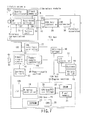
- FIG. 7 is a block diagram of a system that comprises the personal computer 1 and the wireless communication device 2.
- the personal computer 1 has an engine section 34 that controls the other components of the computer 1.
- the engine section 34 comprises a CPU 20, a flash memory 21, a DRAM 22, an EEPROM 23, a CPU bus 24 and a PCI bus 25, and a bus bridge 26.
- the flash memory 21 stores programs including BIOS.
- the DRAM 22 is the main memory of the computer 1.
- the EEPROM 23 is provided to store various items of information such as, but not limited to, configuration information.
- the bus bridge 26 connects the CPU bus 24 and the PCI bus 25.
- the bus bridge 26 incorporates a memory controller designed to control the flash memory 21 and the DRAM 22.
- the bus bridge 26 also incorporates an interface unit, which functions as an interface between the other components of the engine section 34 and a display controller 38.
- the display controller 38 controls the flat panel display 106.
- the personal computer 1 comprises an IDE interface controller 27, a USB host controller 28, a power-supply controller 29, a PCI/ISA bridge 30, an ISA bus 31, an I/O controller 32, various buttons 44, and a rotary switch 45.
- the controllers 27, 28 and 29 and the PCI/ISA bridge 30 are connected to the PCI bus 25.
- the I/O controller 32 is connected to the ISA bus 31 to control the buttons 44 and the rotary switch 45.
- the computer 1 further comprises an HDD 33, a power-supply control circuit 41, and a battery (Li-ion) 42.
- the HDD 33 is connected to the IDE interface controller 27.
- the power-supply control circuit 41 and the power-supply controller 29 constitute a power-supply section 40 that controls the power supply in the personal computer 1.
- the power-supply control circuit 41 generates an operating power from the battery 42 or the output of the AC adapter 43. The operating power is supplied via the power-supply controller 29 to the other components of the computer 1.
- the wireless communication device 2 is a small wireless module that accords with the short-distance wireless communication standard such as BluetoothTM.
- a USB Universal Series Bus
- the USB host controller 28 controls any external USB device to be connected to the USB connector 36.
- a USB interface line 35 connects the controller 28 to the connector 16 provided in the back of the display unit 102.
- the wireless communication device 2 (i.e., a BluetoothTM module) comprises antenna 3, wireless communication IC 7, quartz oscillator 8, flash memory 9, and button cell 3c, as indicated earlier.
- the wireless communication IC 7 has an RF section 37 and a base-band section 39.
- the base-band section controls the wireless communication function of BluetoothTM. It performs the wireless communication between the wireless communication device 2 and an external apparatus (not shown).
- the user can operate the rotary switch 45 to assign a PIN (Personal Identification Number) to the BluetoothTM module 2.
- PIN Personal Identification Number
- FIGS. 8 and 9 are a cross-sectional view and a perspective view, respectively, of this wireless communication device.
- the wireless communication device 2 has a solar cell module 3b embedded in the upper surface of the cover 2a, whereas the wireless communication device 2 of FIGS. 1 to 7 has a button cell 3c provided on the lower surface of the cover 2a.
- the second embodiment is identical to the first embodiment.
- the solar cell module 3b converts light energy to electric energy, which is supplied to the electronic components mounted on the printed circuit board 6.
- the solar cell module 3b is embedded in the upper surface of the cover 2a.
- the light-receiving surface of the cell module 3b lies substantially flush with the upper surface of the cover 2a.
- the module 3b includes a plurality of solar cells (not shown).
- the solar cell module 3b may be shaped like a ring to surround the circumferential surface of the planar antenna module 3.
- a conducting path 100 penetrates the cover 2a, connecting the solar cell module 3b to the printed circuit board 6.
- the power the solar cell module 3b has generated is supplied via the conducting path 100 to the electronic components mounted on the printed circuit board 6.
- the upper surface of the cover 2a remains exposed while the wireless communication device 2 is held in the recess 103 made in the back of the display unit 102, as has been described with reference to FIGS. 1 to 7.
- the solar cell module 3b which is embedded in the upper surface of the cover 2a, can efficiently receive light and can, hence, generate electric power at high efficiency.
- FIG. 10 is a block diagram of a system that comprises the wireless communication device 2 according to the second embodiment and a personal computer 1.
- This personal computer 1 is identical to the personal computer 1 illustrated in FIG. 7.
- the solar cell module 3b is used as a power supply in the wireless communication device 2 according to the second embodiment.
- the power generated by the solar cell module 3b is supplied to the electronic components provided on the printed circuit board 6.
- the wireless communication device 2 of FIGS. 1 to 7 the wireless communication device 2 must be removed from the recess 103 to be replaced by a new button cell.
- the solar cell module 3b need not be replaced as long as it functions well. Hence, the second embodiment is therefore more convenient than the first embodiment.
- FIGS. 11 and 12 are a cross-sectional view and a perspective view, respectively, of this wireless communication device.
- the third embodiment includes a cell box 3d on the lower surface of the printed circuit board 6 and a solar cell module 3b embedded in the upper surface of the cover 2a.
- a button cell 3c can be set into and removed from the cell box 3d.
- the third embodiment is identical to the first embodiment.
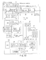
- FIG. 13 is a block diagram of a system that comprises the wireless communication device 2 according to the third embodiment and a personal computer 1.
- This personal computer 1 is identical to the personal computer 1 illustrated in FIG. 7.
- the solar cell module 3b and the button cell 3c are used as power supplies. The power generated by the solar cell module 3b and button cell 3c is supplied to the electronic components provided on the printed circuit board 6.
- the wireless communication device 2 can operate in places where the solar cell module 3b cannot receive sufficient light.
- the recess 103 may be provided in one side of the housing 101 of the computer 1. It suffices to provide the recess 103 in a housing of the information-processing apparatus that functions as the host apparatus to the wireless communication device 2. Then, the wireless communication device 2 can be provided in the apparatus, without protruding from the housing of the apparatus.
Landscapes
- Engineering & Computer Science (AREA)
- Computer Hardware Design (AREA)
- Theoretical Computer Science (AREA)
- Physics & Mathematics (AREA)
- General Engineering & Computer Science (AREA)
- Human Computer Interaction (AREA)
- General Physics & Mathematics (AREA)
- Mathematical Physics (AREA)
- Transceivers (AREA)
- Waveguide Aerials (AREA)
- Support Of Aerials (AREA)
- Transmitters (AREA)
Abstract
a wireless communication device (2) removably provided in the recess (103) and including a planar antenna module (3) having an electromagnetic radiation surface substantially flush with the surface of the information-processing apparatus (1) during operation of the wireless communication device (2).
Description
Claims (6)
- An information-processing apparatus (1) for performing wireless communication, characterized by comprising:a housing having a surface and a recess (103) therein; anda wireless communication device (2) removably provided in the recess (103) and including a planar antenna module (3) having an electromagnetic radiation surface substantially flush with the surface of the information-processing apparatus (1) during operation of the wireless communication device (2).
- The information-processing apparatus (1) according to claim 1, characterized in that the surface of the information-processing apparatus (1) is an outer surface such that the electromagnetic radiation surface is substantially flush with the outer surface during operation of the wireless communication device (2).
- The information-processing apparatus (1) according to claim 1, characterized in that the wireless communication device (2) further includes a printed circuit board (6) including electronic components configured to perform wireless communication.
- The information-processing apparatus (1) according to claim 3, characterized in that the wireless communication device (2) further includes a cover (2a) for covering the printed circuit board (6) and the electronic components.
- The information-processing apparatus (1) according to claim 4, characterized in that the planar antenna module (3) is provided in an upper surface of the cover (2a) such that when the wireless communication device (2) is provided in the recess (103), the upper surface of the cover (2a) and the electromagnetic radiation surface are substantially flush with the surface of the information-processing apparatus (1).
- The information-processing apparatus according to claim 3, characterized in that the wireless communication device (2) further includes a connector (10) provided on a lower surface of the printed circuit board (6) configured to connect the printed circuit board (6) to the information-processing apparatus (1), and a power source (3c) electrically connected to the printed circuit board (6) for supplying electric power to the electronic components.
Applications Claiming Priority (2)
| Application Number | Priority Date | Filing Date | Title |
|---|---|---|---|
| JP2001335421A JP2003140773A (en) | 2001-10-31 | 2001-10-31 | Wireless communication device and information processing apparatus |
| JP2001335421 | 2001-10-31 |
Publications (2)
| Publication Number | Publication Date |
|---|---|
| EP1308824A2 true EP1308824A2 (en) | 2003-05-07 |
| EP1308824A3 EP1308824A3 (en) | 2005-11-02 |
Family
ID=19150415
Family Applications (1)
| Application Number | Title | Priority Date | Filing Date |
|---|---|---|---|
| EP02019445A Withdrawn EP1308824A3 (en) | 2001-10-31 | 2002-08-30 | Wireless communication device and corresponding portable computer |
Country Status (6)
| Country | Link |
|---|---|
| US (1) | US6670926B2 (en) |
| EP (1) | EP1308824A3 (en) |
| JP (1) | JP2003140773A (en) |
| KR (1) | KR20030035854A (en) |
| CN (1) | CN1416222A (en) |
| TW (1) | TWI221949B (en) |
Cited By (6)
| Publication number | Priority date | Publication date | Assignee | Title |
|---|---|---|---|---|
| EP1575124A1 (en) * | 2004-03-11 | 2005-09-14 | Sony Ericsson Mobile Communications AB | Integrated antenna and solar cell assembly and apparatus incorporating same |
| EP1667282A1 (en) * | 2004-12-06 | 2006-06-07 | LG Electronics Inc. | Antenna having radiating part formed flush with surface of casing part |
| CN1300897C (en) * | 2003-05-20 | 2007-02-14 | 华硕电脑股份有限公司 | Electronics with hidden antennas |
| EP1933416A1 (en) * | 2006-12-13 | 2008-06-18 | Alps Electric Co., Ltd. | Antenna-integrated module |
| EP2355238A1 (en) * | 2010-02-10 | 2011-08-10 | HTC Corporation | Handheld device |
| EP3552272A4 (en) * | 2016-12-06 | 2020-07-08 | Commscope Technologies LLC | Antenna radome-enclosures and related antenna structures |
Families Citing this family (82)
| Publication number | Priority date | Publication date | Assignee | Title |
|---|---|---|---|---|
| JP2002032150A (en) * | 2000-05-09 | 2002-01-31 | Sony Corp | Information processing device |
| US20020183009A1 (en) * | 2001-06-01 | 2002-12-05 | Cruz-Albrecht Jose M. | Radio communication within a computer system |
| TW200409401A (en) * | 2002-11-29 | 2004-06-01 | Hon Hai Prec Ind Co Ltd | Antenna assembly and method of the same |
| TW578942U (en) * | 2002-12-31 | 2004-03-01 | Asustek Comp Inc | Printed circuit board antenna assembled inside panel of computer housing |
| FI116334B (en) * | 2003-01-15 | 2005-10-31 | Lk Products Oy | Antenna element |
| TW584292U (en) * | 2003-02-25 | 2004-04-11 | Asustek Comp Inc | Notebook having printed circuit board antenna |
| KR100541440B1 (en) * | 2003-06-02 | 2006-01-10 | 삼성전자주식회사 | Notebook computer |
| JP2005005954A (en) * | 2003-06-11 | 2005-01-06 | Matsushita Electric Ind Co Ltd | antenna |
| US6947001B2 (en) * | 2003-11-18 | 2005-09-20 | Dell Products L.P. | Information handling system including passive RF tuning carrier for wireless modules |
| EP1555864A1 (en) * | 2004-01-14 | 2005-07-20 | Thomson Licensing S.A. | RF circuit with stacked printed circuit boards |
| US20050231900A1 (en) * | 2004-04-16 | 2005-10-20 | Homer Steven S | Portable computer system and method |
| JP3981112B2 (en) * | 2004-10-28 | 2007-09-26 | 株式会社東芝 | Mobile device |
| FI20055420A0 (en) | 2005-07-25 | 2005-07-25 | Lk Products Oy | Adjustable multi-band antenna |
| JP2007043236A (en) * | 2005-07-29 | 2007-02-15 | Ntn Corp | Dielectric antenna |
| FI119009B (en) | 2005-10-03 | 2008-06-13 | Pulse Finland Oy | Multiple-band antenna |
| FI118782B (en) | 2005-10-14 | 2008-03-14 | Pulse Finland Oy | Adjustable antenna |
| JP4746472B2 (en) * | 2006-04-26 | 2011-08-10 | 株式会社東芝 | Information processing apparatus and operation control method thereof |
| JP4357500B2 (en) * | 2006-05-29 | 2009-11-04 | 株式会社東芝 | Information processing device |
| US8618990B2 (en) | 2011-04-13 | 2013-12-31 | Pulse Finland Oy | Wideband antenna and methods |
| US7579993B2 (en) * | 2006-11-01 | 2009-08-25 | Hewlett-Packard Development Company, L.P. | Electronic device detachable antenna assembly |
| JP2008191706A (en) * | 2007-01-31 | 2008-08-21 | Toshiba Corp | Information processing device |
| FI20075269A0 (en) | 2007-04-19 | 2007-04-19 | Pulse Finland Oy | Method and arrangement for antenna matching |
| JP2008294553A (en) * | 2007-05-22 | 2008-12-04 | Univ Of Electro-Communications | Small digital TV tuner unit |
| FI120427B (en) | 2007-08-30 | 2009-10-15 | Pulse Finland Oy | Adjustable multiband antenna |
| JP4756020B2 (en) * | 2007-09-25 | 2011-08-24 | 株式会社東芝 | Housing, method for manufacturing the same, and electronic device |
| CN101425617B (en) * | 2007-10-29 | 2012-11-14 | 英业达股份有限公司 | Electronic device with retractable antenna |
| WO2009107303A1 (en) * | 2008-02-28 | 2009-09-03 | 日本電気株式会社 | Electromagnetic shield structure, wireless device using the structure, and electromagnetic shield manufacturing method |
| JP4469909B1 (en) * | 2008-11-28 | 2010-06-02 | 株式会社東芝 | Electronics |
| DE102009011638B4 (en) * | 2009-03-04 | 2017-05-24 | Fujitsu Technology Solutions Intellectual Property Gmbh | Portable computer |
| TWI405366B (en) * | 2009-05-18 | 2013-08-11 | Quanta Comp Inc | Wireless communciating devide and portable electronic apparatus using the same |
| US20100315297A1 (en) * | 2009-06-12 | 2010-12-16 | Min-Chung Wu | Wireless Device and Method for Manufacturing the Same |
| US9774072B2 (en) * | 2009-10-09 | 2017-09-26 | Htc Corporation | Housing, handheld device, and manufacturing method of housing |
| FI20096134A0 (en) | 2009-11-03 | 2009-11-03 | Pulse Finland Oy | Adjustable antenna |
| FI20096251A0 (en) | 2009-11-27 | 2009-11-27 | Pulse Finland Oy | MIMO antenna |
| US8847833B2 (en) | 2009-12-29 | 2014-09-30 | Pulse Finland Oy | Loop resonator apparatus and methods for enhanced field control |
| CN102157775B (en) * | 2010-02-12 | 2015-01-21 | 宏达国际电子股份有限公司 | handheld device |
| FI20105158A7 (en) | 2010-02-18 | 2011-08-19 | Pulse Finland Oy | ANTENNA EQUIPPED WITH SHELL RADIATOR |
| US8583063B1 (en) | 2010-04-01 | 2013-11-12 | Sprint Communications Company L.P. | Antenna configuration selection by a wireless communication device |
| US9406998B2 (en) | 2010-04-21 | 2016-08-02 | Pulse Finland Oy | Distributed multiband antenna and methods |
| US8686904B2 (en) * | 2010-06-14 | 2014-04-01 | Compal Electronics, Inc. | Antenna-embedded electronic device case |
| KR101705549B1 (en) * | 2010-10-25 | 2017-02-23 | 삼성디스플레이 주식회사 | Display device and wireless transceiver system of image signal including the same |
| FI20115072A0 (en) | 2011-01-25 | 2011-01-25 | Pulse Finland Oy | Multi-resonance antenna, antenna module and radio unit |
| US9673507B2 (en) | 2011-02-11 | 2017-06-06 | Pulse Finland Oy | Chassis-excited antenna apparatus and methods |
| US8648752B2 (en) | 2011-02-11 | 2014-02-11 | Pulse Finland Oy | Chassis-excited antenna apparatus and methods |
| US8866689B2 (en) | 2011-07-07 | 2014-10-21 | Pulse Finland Oy | Multi-band antenna and methods for long term evolution wireless system |
| US9450291B2 (en) | 2011-07-25 | 2016-09-20 | Pulse Finland Oy | Multiband slot loop antenna apparatus and methods |
| CN106935983A (en) * | 2011-09-08 | 2017-07-07 | 英特尔公司 | Overlap and aerial array staggeredly |
| US9123990B2 (en) | 2011-10-07 | 2015-09-01 | Pulse Finland Oy | Multi-feed antenna apparatus and methods |
| US9531058B2 (en) | 2011-12-20 | 2016-12-27 | Pulse Finland Oy | Loosely-coupled radio antenna apparatus and methods |
| US9484619B2 (en) | 2011-12-21 | 2016-11-01 | Pulse Finland Oy | Switchable diversity antenna apparatus and methods |
| US8988296B2 (en) | 2012-04-04 | 2015-03-24 | Pulse Finland Oy | Compact polarized antenna and methods |
| JP6048800B2 (en) * | 2012-09-06 | 2016-12-21 | パナソニックIpマネジメント株式会社 | Contactless power supply system, contactless adapter |
| US9979078B2 (en) | 2012-10-25 | 2018-05-22 | Pulse Finland Oy | Modular cell antenna apparatus and methods |
| CN202917625U (en) * | 2012-10-26 | 2013-05-01 | 中怡(苏州)科技有限公司 | Communication apparatus having integration of antenna and shielding cover |
| US10069209B2 (en) | 2012-11-06 | 2018-09-04 | Pulse Finland Oy | Capacitively coupled antenna apparatus and methods |
| US9647338B2 (en) | 2013-03-11 | 2017-05-09 | Pulse Finland Oy | Coupled antenna structure and methods |
| US10079428B2 (en) | 2013-03-11 | 2018-09-18 | Pulse Finland Oy | Coupled antenna structure and methods |
| US9270011B2 (en) * | 2013-03-15 | 2016-02-23 | Cyberonics, Inc. | Antenna coupled to a cover closing an opening in an implantable medical device |
| US9634383B2 (en) | 2013-06-26 | 2017-04-25 | Pulse Finland Oy | Galvanically separated non-interacting antenna sector apparatus and methods |
| US20150002358A1 (en) * | 2013-06-28 | 2015-01-01 | Samsung Electro-Mechanics Co., Ltd. | Radio communication module |
| JP2015079095A (en) * | 2013-10-16 | 2015-04-23 | 三菱電機株式会社 | Electrical equipment |
| US9680212B2 (en) | 2013-11-20 | 2017-06-13 | Pulse Finland Oy | Capacitive grounding methods and apparatus for mobile devices |
| US9590308B2 (en) | 2013-12-03 | 2017-03-07 | Pulse Electronics, Inc. | Reduced surface area antenna apparatus and mobile communications devices incorporating the same |
| US9350081B2 (en) | 2014-01-14 | 2016-05-24 | Pulse Finland Oy | Switchable multi-radiator high band antenna apparatus |
| US9973228B2 (en) | 2014-08-26 | 2018-05-15 | Pulse Finland Oy | Antenna apparatus with an integrated proximity sensor and methods |
| US9948002B2 (en) | 2014-08-26 | 2018-04-17 | Pulse Finland Oy | Antenna apparatus with an integrated proximity sensor and methods |
| US9722308B2 (en) | 2014-08-28 | 2017-08-01 | Pulse Finland Oy | Low passive intermodulation distributed antenna system for multiple-input multiple-output systems and methods of use |
| WO2016176372A1 (en) * | 2015-04-27 | 2016-11-03 | Osram Sylvania Inc. | Wireless mounted control module |
| US9906260B2 (en) | 2015-07-30 | 2018-02-27 | Pulse Finland Oy | Sensor-based closed loop antenna swapping apparatus and methods |
| CN106940583A (en) * | 2016-01-05 | 2017-07-11 | 宏碁股份有限公司 | Portable electronic device and expandable antenna structure thereof |
| US10651539B2 (en) * | 2016-05-04 | 2020-05-12 | Briggs & Stratton Corporation | Mounting arrangement for wireless communication board for a portable generator |
| USD873249S1 (en) | 2016-12-06 | 2020-01-21 | Commscope Technologies Llc | Antenna radome enclosure and a radome |
| CN107181043B (en) * | 2017-05-22 | 2020-03-27 | 上海安费诺永亿通讯电子有限公司 | Wireless mobile terminal |
| WO2019112608A1 (en) * | 2017-12-08 | 2019-06-13 | Hewlett-Packard Development Company, L.P. | Flexible antenna belts |
| US11936124B2 (en) * | 2018-08-02 | 2024-03-19 | Viasat, Inc. | Antenna element module |
| CN113451740A (en) * | 2020-03-25 | 2021-09-28 | 中兴通讯股份有限公司 | Electronic equipment and shell thereof |
| JP7330143B2 (en) | 2020-06-25 | 2023-08-21 | 株式会社東芝 | disk device |
| JP7286594B2 (en) * | 2020-07-30 | 2023-06-05 | 株式会社東芝 | disk device |
| JP7487132B2 (en) * | 2021-03-18 | 2024-05-20 | 株式会社東芝 | Disk device and electronic device |
| EP4432463A4 (en) * | 2021-11-12 | 2025-03-19 | Panasonic Intellectual Property Management Co., Ltd. | Electronic device |
| JP2023097166A (en) * | 2021-12-27 | 2023-07-07 | 株式会社シマノ | Components for human powered vehicles |
| JP7783782B2 (en) * | 2022-05-23 | 2025-12-10 | シャープ株式会社 | electronic equipment |
Family Cites Families (11)
| Publication number | Priority date | Publication date | Assignee | Title |
|---|---|---|---|---|
| US5440449A (en) * | 1994-01-26 | 1995-08-08 | Intel Corporation | Wireless communication connector and module for notebook personal computers |
| GB2292482A (en) * | 1994-08-18 | 1996-02-21 | Plessey Semiconductors Ltd | Antenna arrangement |
| US5867131A (en) | 1996-11-19 | 1999-02-02 | International Business Machines Corporation | Antenna for a mobile computer |
| JP3562688B2 (en) | 1997-04-08 | 2004-09-08 | 沖電気工業株式会社 | PC card |
| JPH1198046A (en) * | 1997-09-25 | 1999-04-09 | Hitachi Ltd | Information terminal |
| JP2000172376A (en) * | 1998-12-08 | 2000-06-23 | Toshiba Corp | Information processing device |
| FI111420B (en) * | 1999-05-07 | 2003-07-15 | Nokia Corp | Antenna structure in an expansion board for an electronic device |
| JP2001051749A (en) * | 1999-07-30 | 2001-02-23 | Internatl Business Mach Corp <Ibm> | Computer loaded with option unit |
| EP1079296A2 (en) * | 1999-08-06 | 2001-02-28 | Lucent Technologies Inc. | Electronically steerable embedded laptop computer antenna array |
| KR100373686B1 (en) * | 2001-01-31 | 2003-02-25 | 삼성전자주식회사 | A portable computer having external antenna |
| KR20030008853A (en) * | 2001-07-20 | 2003-01-29 | 엘지전자 주식회사 | Detectible wireless antenna module shaped logo type and potable computer |
-
2001
- 2001-10-31 JP JP2001335421A patent/JP2003140773A/en active Pending
-
2002
- 2002-08-30 EP EP02019445A patent/EP1308824A3/en not_active Withdrawn
- 2002-08-30 TW TW091119895A patent/TWI221949B/en not_active IP Right Cessation
- 2002-09-05 US US10/235,415 patent/US6670926B2/en not_active Expired - Fee Related
- 2002-09-11 KR KR1020020054820A patent/KR20030035854A/en not_active Ceased
- 2002-10-22 CN CN02147104A patent/CN1416222A/en active Pending
Cited By (7)
| Publication number | Priority date | Publication date | Assignee | Title |
|---|---|---|---|---|
| CN1300897C (en) * | 2003-05-20 | 2007-02-14 | 华硕电脑股份有限公司 | Electronics with hidden antennas |
| EP1575124A1 (en) * | 2004-03-11 | 2005-09-14 | Sony Ericsson Mobile Communications AB | Integrated antenna and solar cell assembly and apparatus incorporating same |
| EP1667282A1 (en) * | 2004-12-06 | 2006-06-07 | LG Electronics Inc. | Antenna having radiating part formed flush with surface of casing part |
| EP1933416A1 (en) * | 2006-12-13 | 2008-06-18 | Alps Electric Co., Ltd. | Antenna-integrated module |
| EP2355238A1 (en) * | 2010-02-10 | 2011-08-10 | HTC Corporation | Handheld device |
| US9013356B2 (en) | 2010-02-10 | 2015-04-21 | Htc Corporation | Handheld device |
| EP3552272A4 (en) * | 2016-12-06 | 2020-07-08 | Commscope Technologies LLC | Antenna radome-enclosures and related antenna structures |
Also Published As
| Publication number | Publication date |
|---|---|
| EP1308824A3 (en) | 2005-11-02 |
| US6670926B2 (en) | 2003-12-30 |
| TWI221949B (en) | 2004-10-11 |
| US20030080906A1 (en) | 2003-05-01 |
| CN1416222A (en) | 2003-05-07 |
| JP2003140773A (en) | 2003-05-16 |
| KR20030035854A (en) | 2003-05-09 |
Similar Documents
| Publication | Publication Date | Title |
|---|---|---|
| US6670926B2 (en) | Wireless communication device and information-processing apparatus which can hold the device | |
| EP3864829B1 (en) | Antenna using horn structure and electronic device including the same | |
| US7832645B2 (en) | Flash memory card expander | |
| JP3516329B2 (en) | Wireless antenna and mobile computer | |
| CN101443783B (en) | Flash memory card expander | |
| CN1127838C (en) | Honeycomb telephone cell with integrated circuit card | |
| US6788529B2 (en) | Portable computer having multiport bay | |
| JP4647158B2 (en) | Information processing apparatus and external unit | |
| CN111755805A (en) | Antenna modules and electronics | |
| EP3751385B1 (en) | Electronic device including connection structure for electrically connecting printed circuit board and housing | |
| US20210042478A1 (en) | Tray device and electronic device having the same | |
| CN104126248A (en) | Apparatus comprising antenna and ground plane | |
| US20090051621A1 (en) | Antenna structure and related expansion card and computer apparatus | |
| JP4669460B2 (en) | Electronic equipment and sheet metal parts | |
| EP1276299A2 (en) | Portable information terminal | |
| KR101084945B1 (en) | Card battery and connector on the card battery | |
| US8242743B2 (en) | Mouse with battery chamber and battery charging circuit | |
| US9965664B2 (en) | Mobile data collector with keyboard | |
| US6510057B2 (en) | Computing device with a card receptacle | |
| JP2003272582A (en) | Card-type battery device and electronic apparatus using the same | |
| JP3109383U (en) | Portable power supply device with computer port | |
| US20090037632A1 (en) | Rechargeable wireless portable device | |
| US20060046779A1 (en) | Method and apparatus for providing enhanced functionality for a mobile communication device | |
| JP2000134021A (en) | Portable radio | |
| US8289704B2 (en) | Electronic apparatus |
Legal Events
| Date | Code | Title | Description |
|---|---|---|---|
| PUAI | Public reference made under article 153(3) epc to a published international application that has entered the european phase |
Free format text: ORIGINAL CODE: 0009012 |
|
| 17P | Request for examination filed |
Effective date: 20020830 |
|
| AK | Designated contracting states |
Designated state(s): AT BE BG CH CY CZ DE DK EE ES FI FR GB GR IE IT LI LU MC NL PT SE SK TR |
|
| AX | Request for extension of the european patent |
Extension state: AL LT LV MK RO SI |
|
| PUAL | Search report despatched |
Free format text: ORIGINAL CODE: 0009013 |
|
| AK | Designated contracting states |
Kind code of ref document: A3 Designated state(s): AT BE BG CH CY CZ DE DK EE ES FI FR GB GR IE IT LI LU MC NL PT SE SK TR |
|
| AX | Request for extension of the european patent |
Extension state: AL LT LV MK RO SI |
|
| RIC1 | Information provided on ipc code assigned before grant |
Ipc: 7H 01Q 1/22 B Ipc: 7G 06F 1/16 A |
|
| AKX | Designation fees paid |
Designated state(s): DE FR GB |
|
| STAA | Information on the status of an ep patent application or granted ep patent |
Free format text: STATUS: THE APPLICATION IS DEEMED TO BE WITHDRAWN |
|
| 18D | Application deemed to be withdrawn |
Effective date: 20060619 |