EP1308476A1 - Insulation film forming material, insulation film, method for forming the insulation film, and semiconductor device - Google Patents
Insulation film forming material, insulation film, method for forming the insulation film, and semiconductor device Download PDFInfo
- Publication number
- EP1308476A1 EP1308476A1 EP02006791A EP02006791A EP1308476A1 EP 1308476 A1 EP1308476 A1 EP 1308476A1 EP 02006791 A EP02006791 A EP 02006791A EP 02006791 A EP02006791 A EP 02006791A EP 1308476 A1 EP1308476 A1 EP 1308476A1
- Authority
- EP
- European Patent Office
- Prior art keywords
- poly
- insulation film
- film
- compound
- silicon compound
- Prior art date
- Legal status (The legal status is an assumption and is not a legal conclusion. Google has not performed a legal analysis and makes no representation as to the accuracy of the status listed.)
- Granted
Links
Images


Classifications
-
- H—ELECTRICITY
- H10—SEMICONDUCTOR DEVICES; ELECTRIC SOLID-STATE DEVICES NOT OTHERWISE PROVIDED FOR
- H10P—GENERIC PROCESSES OR APPARATUS FOR THE MANUFACTURE OR TREATMENT OF DEVICES COVERED BY CLASS H10
- H10P14/00—Formation of materials, e.g. in the shape of layers or pillars
- H10P14/60—Formation of materials, e.g. in the shape of layers or pillars of insulating materials
- H10P14/69—Inorganic materials
- H10P14/692—Inorganic materials composed of oxides, glassy oxides or oxide-based glasses
- H10P14/6921—Inorganic materials composed of oxides, glassy oxides or oxide-based glasses containing silicon
- H10P14/6922—Inorganic materials composed of oxides, glassy oxides or oxide-based glasses containing silicon the material containing Si, O and at least one of H, N, C, F or other non-metal elements, e.g. SiOC, SiOC:H or SiONC
-
- H—ELECTRICITY
- H10—SEMICONDUCTOR DEVICES; ELECTRIC SOLID-STATE DEVICES NOT OTHERWISE PROVIDED FOR
- H10P—GENERIC PROCESSES OR APPARATUS FOR THE MANUFACTURE OR TREATMENT OF DEVICES COVERED BY CLASS H10
- H10P14/00—Formation of materials, e.g. in the shape of layers or pillars
- H10P14/60—Formation of materials, e.g. in the shape of layers or pillars of insulating materials
-
- C—CHEMISTRY; METALLURGY
- C09—DYES; PAINTS; POLISHES; NATURAL RESINS; ADHESIVES; COMPOSITIONS NOT OTHERWISE PROVIDED FOR; APPLICATIONS OF MATERIALS NOT OTHERWISE PROVIDED FOR
- C09D—COATING COMPOSITIONS, e.g. PAINTS, VARNISHES OR LACQUERS; FILLING PASTES; CHEMICAL PAINT OR INK REMOVERS; INKS; CORRECTING FLUIDS; WOODSTAINS; PASTES OR SOLIDS FOR COLOURING OR PRINTING; USE OF MATERIALS THEREFOR
- C09D183/00—Coating compositions based on macromolecular compounds obtained by reactions forming in the main chain of the macromolecule a linkage containing silicon, with or without sulfur, nitrogen, oxygen, or carbon only; Coating compositions based on derivatives of such polymers
- C09D183/14—Coating compositions based on macromolecular compounds obtained by reactions forming in the main chain of the macromolecule a linkage containing silicon, with or without sulfur, nitrogen, oxygen, or carbon only; Coating compositions based on derivatives of such polymers in which at least two but not all the silicon atoms are connected by linkages other than oxygen atoms
-
- C—CHEMISTRY; METALLURGY
- C09—DYES; PAINTS; POLISHES; NATURAL RESINS; ADHESIVES; COMPOSITIONS NOT OTHERWISE PROVIDED FOR; APPLICATIONS OF MATERIALS NOT OTHERWISE PROVIDED FOR
- C09D—COATING COMPOSITIONS, e.g. PAINTS, VARNISHES OR LACQUERS; FILLING PASTES; CHEMICAL PAINT OR INK REMOVERS; INKS; CORRECTING FLUIDS; WOODSTAINS; PASTES OR SOLIDS FOR COLOURING OR PRINTING; USE OF MATERIALS THEREFOR
- C09D183/00—Coating compositions based on macromolecular compounds obtained by reactions forming in the main chain of the macromolecule a linkage containing silicon, with or without sulfur, nitrogen, oxygen, or carbon only; Coating compositions based on derivatives of such polymers
- C09D183/16—Coating compositions based on macromolecular compounds obtained by reactions forming in the main chain of the macromolecule a linkage containing silicon, with or without sulfur, nitrogen, oxygen, or carbon only; Coating compositions based on derivatives of such polymers in which all the silicon atoms are connected by linkages other than oxygen atoms
-
- H—ELECTRICITY
- H10—SEMICONDUCTOR DEVICES; ELECTRIC SOLID-STATE DEVICES NOT OTHERWISE PROVIDED FOR
- H10P—GENERIC PROCESSES OR APPARATUS FOR THE MANUFACTURE OR TREATMENT OF DEVICES COVERED BY CLASS H10
- H10P14/00—Formation of materials, e.g. in the shape of layers or pillars
- H10P14/60—Formation of materials, e.g. in the shape of layers or pillars of insulating materials
- H10P14/65—Formation of materials, e.g. in the shape of layers or pillars of insulating materials characterised by treatments performed before or after the formation of the materials
- H10P14/6502—Formation of materials, e.g. in the shape of layers or pillars of insulating materials characterised by treatments performed before or after the formation of the materials of treatments performed before formation of the materials
- H10P14/6506—Formation of intermediate materials
-
- H—ELECTRICITY
- H10—SEMICONDUCTOR DEVICES; ELECTRIC SOLID-STATE DEVICES NOT OTHERWISE PROVIDED FOR
- H10P—GENERIC PROCESSES OR APPARATUS FOR THE MANUFACTURE OR TREATMENT OF DEVICES COVERED BY CLASS H10
- H10P14/00—Formation of materials, e.g. in the shape of layers or pillars
- H10P14/60—Formation of materials, e.g. in the shape of layers or pillars of insulating materials
- H10P14/65—Formation of materials, e.g. in the shape of layers or pillars of insulating materials characterised by treatments performed before or after the formation of the materials
- H10P14/6516—Formation of materials, e.g. in the shape of layers or pillars of insulating materials characterised by treatments performed before or after the formation of the materials of treatments performed after formation of the materials
- H10P14/6529—Formation of materials, e.g. in the shape of layers or pillars of insulating materials characterised by treatments performed before or after the formation of the materials of treatments performed after formation of the materials by exposure to a gas or vapour
-
- H—ELECTRICITY
- H10—SEMICONDUCTOR DEVICES; ELECTRIC SOLID-STATE DEVICES NOT OTHERWISE PROVIDED FOR
- H10P—GENERIC PROCESSES OR APPARATUS FOR THE MANUFACTURE OR TREATMENT OF DEVICES COVERED BY CLASS H10
- H10P14/00—Formation of materials, e.g. in the shape of layers or pillars
- H10P14/60—Formation of materials, e.g. in the shape of layers or pillars of insulating materials
- H10P14/65—Formation of materials, e.g. in the shape of layers or pillars of insulating materials characterised by treatments performed before or after the formation of the materials
- H10P14/6516—Formation of materials, e.g. in the shape of layers or pillars of insulating materials characterised by treatments performed before or after the formation of the materials of treatments performed after formation of the materials
- H10P14/6548—Formation of materials, e.g. in the shape of layers or pillars of insulating materials characterised by treatments performed before or after the formation of the materials of treatments performed after formation of the materials by forming intermediate materials, e.g. capping layers or diffusion barriers
-
- H—ELECTRICITY
- H10—SEMICONDUCTOR DEVICES; ELECTRIC SOLID-STATE DEVICES NOT OTHERWISE PROVIDED FOR
- H10P—GENERIC PROCESSES OR APPARATUS FOR THE MANUFACTURE OR TREATMENT OF DEVICES COVERED BY CLASS H10
- H10P14/00—Formation of materials, e.g. in the shape of layers or pillars
- H10P14/60—Formation of materials, e.g. in the shape of layers or pillars of insulating materials
- H10P14/66—Formation of materials, e.g. in the shape of layers or pillars of insulating materials characterised by the type of materials
- H10P14/668—Formation of materials, e.g. in the shape of layers or pillars of insulating materials characterised by the type of materials the materials being characterised by the deposition precursor materials
- H10P14/6681—Formation of materials, e.g. in the shape of layers or pillars of insulating materials characterised by the type of materials the materials being characterised by the deposition precursor materials the precursor containing a compound comprising Si
- H10P14/6682—Formation of materials, e.g. in the shape of layers or pillars of insulating materials characterised by the type of materials the materials being characterised by the deposition precursor materials the precursor containing a compound comprising Si the compound being a silane, e.g. disilane, methylsilane or chlorosilane
-
- H—ELECTRICITY
- H10—SEMICONDUCTOR DEVICES; ELECTRIC SOLID-STATE DEVICES NOT OTHERWISE PROVIDED FOR
- H10W—GENERIC PACKAGES, INTERCONNECTIONS, CONNECTORS OR OTHER CONSTRUCTIONAL DETAILS OF DEVICES COVERED BY CLASS H10
- H10W20/00—Interconnections in chips, wafers or substrates
- H10W20/01—Manufacture or treatment
- H10W20/071—Manufacture or treatment of dielectric parts thereof
-
- H—ELECTRICITY
- H10—SEMICONDUCTOR DEVICES; ELECTRIC SOLID-STATE DEVICES NOT OTHERWISE PROVIDED FOR
- H10W—GENERIC PACKAGES, INTERCONNECTIONS, CONNECTORS OR OTHER CONSTRUCTIONAL DETAILS OF DEVICES COVERED BY CLASS H10
- H10W20/00—Interconnections in chips, wafers or substrates
- H10W20/01—Manufacture or treatment
- H10W20/071—Manufacture or treatment of dielectric parts thereof
- H10W20/081—Manufacture or treatment of dielectric parts thereof by forming openings in the dielectric parts
- H10W20/084—Manufacture or treatment of dielectric parts thereof by forming openings in the dielectric parts for dual-damascene structures
-
- H—ELECTRICITY
- H10—SEMICONDUCTOR DEVICES; ELECTRIC SOLID-STATE DEVICES NOT OTHERWISE PROVIDED FOR
- H10W—GENERIC PACKAGES, INTERCONNECTIONS, CONNECTORS OR OTHER CONSTRUCTIONAL DETAILS OF DEVICES COVERED BY CLASS H10
- H10W20/00—Interconnections in chips, wafers or substrates
- H10W20/40—Interconnections external to wafers or substrates, e.g. back-end-of-line [BEOL] metallisations or vias connecting to gate electrodes
- H10W20/45—Interconnections external to wafers or substrates, e.g. back-end-of-line [BEOL] metallisations or vias connecting to gate electrodes characterised by their insulating parts
- H10W20/47—Interconnections external to wafers or substrates, e.g. back-end-of-line [BEOL] metallisations or vias connecting to gate electrodes characterised by their insulating parts comprising two or more dielectric layers having different properties, e.g. different dielectric constants
-
- H—ELECTRICITY
- H10—SEMICONDUCTOR DEVICES; ELECTRIC SOLID-STATE DEVICES NOT OTHERWISE PROVIDED FOR
- H10W—GENERIC PACKAGES, INTERCONNECTIONS, CONNECTORS OR OTHER CONSTRUCTIONAL DETAILS OF DEVICES COVERED BY CLASS H10
- H10W20/00—Interconnections in chips, wafers or substrates
- H10W20/40—Interconnections external to wafers or substrates, e.g. back-end-of-line [BEOL] metallisations or vias connecting to gate electrodes
- H10W20/45—Interconnections external to wafers or substrates, e.g. back-end-of-line [BEOL] metallisations or vias connecting to gate electrodes characterised by their insulating parts
- H10W20/48—Insulating materials thereof
-
- H—ELECTRICITY
- H10—SEMICONDUCTOR DEVICES; ELECTRIC SOLID-STATE DEVICES NOT OTHERWISE PROVIDED FOR
- H10W—GENERIC PACKAGES, INTERCONNECTIONS, CONNECTORS OR OTHER CONSTRUCTIONAL DETAILS OF DEVICES COVERED BY CLASS H10
- H10W20/00—Interconnections in chips, wafers or substrates
- H10W20/40—Interconnections external to wafers or substrates, e.g. back-end-of-line [BEOL] metallisations or vias connecting to gate electrodes
- H10W20/495—Capacitive arrangements or effects of, or between wiring layers
-
- H—ELECTRICITY
- H10—SEMICONDUCTOR DEVICES; ELECTRIC SOLID-STATE DEVICES NOT OTHERWISE PROVIDED FOR
- H10P—GENERIC PROCESSES OR APPARATUS FOR THE MANUFACTURE OR TREATMENT OF DEVICES COVERED BY CLASS H10
- H10P14/00—Formation of materials, e.g. in the shape of layers or pillars
- H10P14/60—Formation of materials, e.g. in the shape of layers or pillars of insulating materials
- H10P14/63—Formation of materials, e.g. in the shape of layers or pillars of insulating materials characterised by the formation processes
- H10P14/6326—Deposition processes
- H10P14/6342—Liquid deposition, e.g. spin-coating, sol-gel techniques or spray coating
-
- H—ELECTRICITY
- H10—SEMICONDUCTOR DEVICES; ELECTRIC SOLID-STATE DEVICES NOT OTHERWISE PROVIDED FOR
- H10P—GENERIC PROCESSES OR APPARATUS FOR THE MANUFACTURE OR TREATMENT OF DEVICES COVERED BY CLASS H10
- H10P14/00—Formation of materials, e.g. in the shape of layers or pillars
- H10P14/60—Formation of materials, e.g. in the shape of layers or pillars of insulating materials
- H10P14/66—Formation of materials, e.g. in the shape of layers or pillars of insulating materials characterised by the type of materials
- H10P14/665—Porous materials
-
- H—ELECTRICITY
- H10—SEMICONDUCTOR DEVICES; ELECTRIC SOLID-STATE DEVICES NOT OTHERWISE PROVIDED FOR
- H10P—GENERIC PROCESSES OR APPARATUS FOR THE MANUFACTURE OR TREATMENT OF DEVICES COVERED BY CLASS H10
- H10P14/00—Formation of materials, e.g. in the shape of layers or pillars
- H10P14/60—Formation of materials, e.g. in the shape of layers or pillars of insulating materials
- H10P14/66—Formation of materials, e.g. in the shape of layers or pillars of insulating materials characterised by the type of materials
- H10P14/668—Formation of materials, e.g. in the shape of layers or pillars of insulating materials characterised by the type of materials the materials being characterised by the deposition precursor materials
- H10P14/6681—Formation of materials, e.g. in the shape of layers or pillars of insulating materials characterised by the type of materials the materials being characterised by the deposition precursor materials the precursor containing a compound comprising Si
- H10P14/6684—Formation of materials, e.g. in the shape of layers or pillars of insulating materials characterised by the type of materials the materials being characterised by the deposition precursor materials the precursor containing a compound comprising Si the compound comprising silicon and oxygen
- H10P14/6686—Formation of materials, e.g. in the shape of layers or pillars of insulating materials characterised by the type of materials the materials being characterised by the deposition precursor materials the precursor containing a compound comprising Si the compound comprising silicon and oxygen the compound being a molecule comprising at least one silicon-oxygen bond and the compound having hydrogen or an organic group attached to the silicon or oxygen, e.g. a siloxane
-
- H—ELECTRICITY
- H10—SEMICONDUCTOR DEVICES; ELECTRIC SOLID-STATE DEVICES NOT OTHERWISE PROVIDED FOR
- H10W—GENERIC PACKAGES, INTERCONNECTIONS, CONNECTORS OR OTHER CONSTRUCTIONAL DETAILS OF DEVICES COVERED BY CLASS H10
- H10W20/00—Interconnections in chips, wafers or substrates
- H10W20/01—Manufacture or treatment
- H10W20/071—Manufacture or treatment of dielectric parts thereof
- H10W20/072—Manufacture or treatment of dielectric parts thereof of dielectric parts comprising air gaps
-
- H—ELECTRICITY
- H10—SEMICONDUCTOR DEVICES; ELECTRIC SOLID-STATE DEVICES NOT OTHERWISE PROVIDED FOR
- H10W—GENERIC PACKAGES, INTERCONNECTIONS, CONNECTORS OR OTHER CONSTRUCTIONAL DETAILS OF DEVICES COVERED BY CLASS H10
- H10W20/00—Interconnections in chips, wafers or substrates
- H10W20/40—Interconnections external to wafers or substrates, e.g. back-end-of-line [BEOL] metallisations or vias connecting to gate electrodes
- H10W20/41—Interconnections external to wafers or substrates, e.g. back-end-of-line [BEOL] metallisations or vias connecting to gate electrodes characterised by their conductive parts
- H10W20/425—Barrier, adhesion or liner layers
Definitions
- the present invention relates to an insulation film material which can form a porous insulation film of high mechanical strength and low dielectric constant, an insulation film, method for forming the insulation film, and a semiconductor device.
- the interconnection delay has not generally much influenced the devices.
- the interconnection gaps become below 1 ⁇ m as semiconductor integrated circuits are more integrated, the influence of the interconnection delay on the device velocity cannot be bypassed.
- the interconnection delay caused by parasitic capacities among interconnections will have much influence on the device velocity.
- an interconnection delay T is influenced by an interconnection resistance R and an interconnection capacitance C and expressed by the following formula. T ⁇ CR
- An interconnection capacitance C is expressed by the following formula where an electrode area is represented by S; an interconnection gap, d; vacuum dielectric constant, ⁇ 0 ; and an interconnection insulation film dielectric constant, ⁇ r .
- C ⁇ 0 ⁇ r S d
- silicon dioxide SiO 2 silicon dioxide
- silicon nitride SiN silicon nitride
- phospho silicate glass PSG etc.
- Silicon oxide film which is the most popular in semiconductor devices, and which is formed by chemical vapor deposition (CVD) has an about 4 of dielectric constant.
- silica-based porous films having a number of pores formed in the films for lower dielectric constants as the interconnection insulation film is considered.
- SiOF films formed by CVD have dielectric constant values ranging from about 3.3 to 3.5 and it is difficult to form SiOF films of dielectric constant values of below 3.
- the interconnection capacitance cannot be sufficiently reduced.
- SiOF films have high hygroscopicity and often have increased dielectric constants after formed.
- organic polymers such as polyimide, etc. have low dielectric constants ranging from about 2 to 3.
- organic polymers are insufficient in heat resistance and adhesion and have restricted fabrication processes for semiconductor devices.
- silica-based porous film has pores formed by applying to a substrate a material including a siloxane resin and a pyrolytic resin and sintering the material.
- silica-based porous film when a pore volume in the film is increased for lower dielectric constant, the film has the mechanical strength extremely lowered.
- a porosity of the film In order to form a porous film of, e.g., a below 2.0- dielectric constant, a porosity of the film must be above 50 %. Disadvantageously, the film tends to be broken in the processes of chemical mechanical polishing (CMP), etc.
- CMP chemical mechanical polishing
- the film has also a disadvantage of high hygroscopicity. Accordingly, silica-based porous film cannot have sufficient properties for forming insulation films of low dielectric constants which are essential to realize high-velocity semiconductor devices.
- an insulation film forming material comprising: a silicon compound having a skeleton of C-C bonds; a porous forming compound which is decomposed or evaporated by a heat treatment; and a solvent which dissolves the silicon compound with the porous forming material.
- an insulation film comprising a film of a silicon compound having a skeleton containing C-C bonds, wherein pores of below 10 nm-size are formed in the film.
- a method for forming an insulation film comprising the steps of: applying to a substrate an insulation film forming material including a silicon compound having a skeleton containing C-C bonds, a pore forming compound which is decomposed or evaporated by a heat treatment and a solvent which dissolves the silicon compound and the pore forming compound; drying the insulation film forming material applied to the substrate to form a film containing the silicon compound and the pore forming compound; and decomposing or evaporating the pore forming compound by subjecting the substrate to the heat treatment to eliminate the pore forming compound from the film to form pores in the film.
- a semiconductor device comprising a porous insulation film comprising a film of a silicon compound having a skeleton containing C-C bonds formed on a semiconductor substrate, wherein pores of below 10 nm-size are formed in the film.
- a porous insulation film is formed of an insulation film forming material including a silicon compound having a skeleton containing C-C bonds, a pore forming compound which is decomposed or evaporated by a heat treatment, a solvent for dissolving the silicon compound and the pore forming compound, whereby the porous insulation film can have good mechanical strength and low dielectric constant.
- FIGs. 2A and 2B are graphs of relationships among porosities, dielectric constants and mechanical strengths of porous insulation films formed of the insulation film forming material according to examples of the present invention (Part 2).
- FIG. 3 is a sectional view of the semiconductor device using the porous insulation film formed of the insulation film forming material according to the present invention as inter-layer insulation films of a multi-interconnection layer structure, which shows a structure of the semiconductor device.
- FIGs. 4A-4D are sectional views of the semiconductor device using the porous insulation film formed of the insulation film forming material according to the present invention as inter-layer insulation films of a multi-interconnection layer structure in the steps of the method for fabricating the semiconductor device, which explain the method (Part 1).
- FIGs. 5A and 5B are sectional views of the semiconductor device using the porous insulation film formed of the insulation film forming material according to the present invention as inter-layer insulation films of a multi-interconnection layer structure in the steps of the method for fabricating the semiconductor device, which explain the method (Part 2).
- the insulation film forming material according to the present invention is characterized mainly by including a silicon compound having a skeleton containing C-C bonds, a pore forming compound which is decomposed or evaporated with a heat treatment, and a solvent for dissolving the silicon compound and the pore forming compound.
- Inter-layer insulation films for the interconnection layers of semiconductor devices are required to have low dielectric constants for the purpose of reducing the parasitic capacity among the interconnections and depressing generation of interconnection delay.
- Silica-based porous insulation films formed of siloxane resins and pyrolytic resins can realize low dielectric constants by forming pores in the films.
- the porous insulation films can be insulation films of lower dielectric constants by increasing pore volumes in the films, i.e. by increasing porosities of the films.
- increase of porosities of the films lowers mechanical strengths thereof. This has made it difficult to use CMP, which exerts large mechanical loads.
- the silica-based porous insulation films have thus restricted fabrication processes for semiconductor devices. As a result, even the porous insulation films have not been able to be insulation films of semiconductor devices of sufficiently lower dielectric constants.
- the inventors of the present invention have so far made earnest studies of insulation film forming materials which will substitute siloxane resin.
- a silicon compound having a skeleton containing C-C bonds has a silicon atom to oxygen atom ratio of 1 : 0 - 0.5, whereby a film of a below 2.6 dielectric constant can be produced.
- substrate which itself has low dielectric constant, can have low dielectric constant even when a porosity is low, whereby decrease of the film strength with increase of the porosity can be depressed.
- the porous insulation film formed of such silicon compound have characteristics of high humidity resistance and chemical resistance.
- a porous insulation film is formed of the above-described silicon compound having a skeleton containing C-C bonds, whereby the porous insulation film can have low dielectric constant and high mechanical strength.
- a substrate means not only a semiconductor substrate itself, but also a semiconductor substrate with transistors, interconnection layers, etc. formed on.
- the insulation film forming material according to the present invention includes a silicon compound having a skeleton containing C-C bonds, a pore forming compound which functions as an elimination agent for forming pores in the film, and a diluent for both compounds.
- the respective components of the insulation forming material according to the present invention will be detailed below.
- the silicon compound having a skeleton containing C-C bonds can be, e.g., poly(dimethylcarbosilane), poly(hydromethylcarbosilane), poly(diethylcarbosilane), poly(hydroethylcarbosilane), poly(carbosilastyrene), poly(phenylmethylcarbosilane), poly(diphenylcarbosilane), poly(dimethylsilphenylenesiloxane), poly(methylsilphenylenesiloxane), poly(diethylsilphenylenesiloxane), poly(ethylsilphenylenesiloxane), poly(dipropylsilphenylenesiloxane), poly(propylsilphenylenesiloxane), poly(propylsilphenylenesiloxane), poly(propylsilphenylenesiloxane), poly(propylsilphenylene
- the silicon compound preferably has the structure expressed by the following general formula. (Either of R 1 and R 2 is hydrogen, and the other is hydrocarbon having 1 - 3 carbon atoms or a phenyl group. R 3 is hydrocarbon having 1 - 3 carbon atoms or a phenylene group, or oxygen. o is an integer of 20 - 1000.)
- the silicon compound has hydrogen in the side chains.
- the side chains enable the silicon compound to react with the amine compound having 4 or more carbon atoms as the pore forming compound which will be described below to form micronized pores in the film.
- the pore forming compound is not especially limited as long as it is an amine compound having 4 or more carbon atoms, and can be, e.g., aminobutane, diaminobutane, cyclohexylamine, dicyclohexylamine, tetramethylammoniun hydride, hexamethylammonium hydride, hexadecylammonium hydride, or others.
- quaternary amine whose reactivity with silicon-hydrogen bonds is high, is used.
- a generally used elimination agent such as polyethylene resin or others may be used.
- the diluent is not especially limited as long as the diluent can dissolve the above-described silicon compound and the pore forming compound.
- the diluent can be, e.g., cyclohexanone, methyl isobutyl ketone, methyl ethyl ketone, methyl cellosolve, ethyl cellosolve, octane, decane, propylene glycol, propylene glycol monomethyl ether, propylene glycol monomethyl ether acetate, diethylene glycol, propylene glycol, propylene glycol monomethyl ether, propylene glycol monoethyl ether, propylene glycol monopropylether, or others.
- the insulation film forming material according to the present invention will be applied, by, e.g., spin coating, to a substrate for the porous insulation film to be formed on.
- the substrate with the insulation film forming material applied to is annealed at, e.g., 50 - 350 °C.
- the solvent is evaporated and the pore forming compound is partially eliminated by heating.
- the porous insulation film formed on the substrate is heat-treated at, e.g., 300 - 500 °C in an atmosphere of a 5 % oxygen concentration. Thus, the formation of the porous insulation film is completed.
- the thus formed porous insulation film has characteristics of high chemical resistance to acid and alkaline chemicals, etc., and high humidity resistance.
- a dielectric constant value of the porous insulation film is below 2.0 even when a porosity of the porous insulation film is about 30 %. Accordingly, in comparison with the conventional silica-based porous insulation film, the porous insulation film has smaller strength reduction due to the pores in the porous insulation film.
- the above-described the insulation film forming method is applicable to forming inter-layer insulation film, etc. of semiconductor devices of multi-interconnection layer structure.
- the porous insulation film As described above, according to the present embodiment, as a material of the porous insulation film a silicon compound having a skeleton containing C-C bonds is used, whereby the porous insulation film of low dielectric constant can have high mechanical strength, and high chemical resistance and high humidity resistance.
- Methylhydropolycarbosilane is dissolved by 10 % in 90 g of methyisobutylketone to be loaded in a 300 ml-three-necked flask equipped with a Dimroth condenser and agitating blades.
- An aqueous solution of 5 % tetramethyl ammonium hydride was dropped in the solution by 20 g at 40 °C. After the drop, the solution was left at 40 °C for 2 hours and was cooled to the room temperature. Then magnesium sulfate was added by 30 g and dehydrated.
- the insulation film forming material was prepared.
- Methylhydropolycarbosilane is dissolved by 10 % in 90 g of methyisobutylketone to be loaded in a 300 ml-three-necked flask equipped with a Dimroth condenser and agitating blades.
- An aqueous solution of 5 % tetramethyl ammonium hydride was dropped in the solution by 40 g at 40 °C. After the drop, the solution was left at 40 °C for 2 hours and was cooled to the room temperature. Then magnesium sulfate was added by 30 g and dehydrated.
- the insulation film forming material was prepared in the same way as in Example 1 except that the aqueous solution of tetramethyl ammmonium hydride which was dropped by 20 g in Example 1 was dropped by 40 g.
- Methylhydropolycarbosilane is dissolved by 10 % in 90 g of methyisobutylketone to be loaded in a 300 ml-three-necked flask equipped with a Dimroth condenser and agitating blades.
- An aqueous solution of 5 % tetramethyl ammonium hydride was dropped in the solution by 60 g at 40 °C. After the drop, the solution was left at 40 °C for 2 hours and was cooled to the room temperature. Then magnesium sulfate was added by 30 g and dehydrated.
- the insulation film forming material was prepared in the same way as in Example 1 except that the aqueous solution of tetramethyl ammmonium hydride which was dropped by 20 g in Example 1 was dropped by 60 g.
- Methylhydropolycarbosilane is dissolved by 10 % in 90 g of methyisobutylketone to be loaded in a 300 ml-three-necked flask equipped with a Dimroth condenser and agitating blades.
- An aqueous solution of 5 % tetramethyl ammonium hydride was dropped in the solution by 100 g at 40 °C. After the drop, the solution was left at 40 °C for 2 hours and was cooled to the room temperature. Then magnesium sulfate was added by 30 g and dehydrated.
- the insulation film forming material was prepared in the same way as in Example 1 except that the aqueous solution of tetramethyl ammmonium hydride which was dropped by 20 g in Example 1 was dropped by 100 g.
- Methylhydropolycarbosilane is dissolved by 10 % in 90 g of methyisobutylketone to be loaded in a 300 ml-three-necked flask equipped with a Dimroth condenser and agitating blades.
- a methylisobutylketone solution of 5 % polystyrene resin was dropped in the solution by 20 g at 40 °C. After the drop, the solution was left at 40 °C for 2 hours and was cooled to the room temperature.
- the insulation film forming material was prepared.
- Methylhydropolycarbosilane is dissolved by 10 % in 90 g of methyisobutylketone to be loaded in a 300 ml-three-necked flask equipped with a Dimroth condenser and agitating blades.
- a methylisobutylketone solution of 5 % polystyrene resin was dropped in the solution by 40 g at 40 °C. After the drop, the solution was left at 40 °C for 2 hours and was cooled to the room temperature.
- the insulation film forming material was prepared in the same way as in Example 5 except that the methylisobutylketone solution of 5 % polystyrene resin which was dropped by 20 g in Example 1 was dropped by 40 g.
- Methylhydropolycarbosilane is dissolved by 10 % in 90 g of methyisobutylketone to be loaded in a 300 ml-three-necked flask equipped with a Dimroth condenser and agitating blades.
- a methylisobutylketone solution of 5 % polystyrene resin was dropped in the solution by 60 g at 40 °C. After the drop, the solution was left at 40 °C for 2 hours and was cooled to the room temperature.
- the insulation film forming material was prepared in the same way as in Example 5 except that the methylisobutylketone solution of 5 % polystyrene resin which was dropped by 20 g in Example 1 was dropped by 60 g.
- Methylhydropolycarbosilane is dissolved by 10 % in 90 g of methyisobutylketone to be loaded in a 300 ml-three-necked flask equipped with a Dimroth condenser and agitating blades.
- a methylisobutylketone solution of 5 % polystyrene resin was dropped in the solution by 100 g at 40 °C. After the drop, the solution was left at 40 °C for 2 hours and was cooled to the room temperature.
- the insulation film forming material was prepared in the same way as in Example 5 except that the methylisobutylketone solution of 5 % polystyrene resin which was dropped by 20 g in Example 1 was dropped by 100 g.
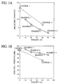
- Porous insulation films were formed of the insulation film forming materials prepared in Examples 1 to 8 and Controls 1 and 2. Dielectric constants of the respective porous insulation films, and relationships between mechanical strength and porosity of the respective porous insulation films were measured.
- the porous insulation films for measuring dielectric constants and mechanical strength were formed as follows:
- the insulation film forming materials were applied to silicon wafers by spin coating at a 3000 rotation number for 20 seconds. Then, the solvent was dried at 200 °C, and next the silicon wafers were sintered at 200 °C for 30 minutes in a nitrogen atmosphere of a 5000 ppm-oxygen concentration. Thus, the porous insulation films were formed on the silicon substrates.
- a 1 mm Au-electrode was formed on the porous insulation film thus formed of the respective insulation film forming materials, and capacitances and voltage characteristics were measured to compute dielectric constant values.
- FIG. 1A is a graph of the dielectric constant values computed on the porous insulation films formed of the insulation film forming materials according to Examples 1 to 4 plotted with respect to porosities.
- FIG. 2A is a graph of dielectric constant values computed on the porous insulation films formed of the insulation film forming materials of Examples 5 to 8 plotted with respect to porosities of the porous insulation films.
- porous insulation forming materials of the respective examples have lower dielectric constants for substantially the same porosity in comparison with the porous insulation film forming materials of the controls.
- a 100 nm-plasma silicon nitride film is formed as a cap film on the porous insulation films formed of the insulation films of the respective examples, and a stud-pull test was made to measure mechanical strength of the porous insulation films.
- FIG. 1B is a graph of mechanical strengths measured on the porous insulation films formed of the insulation film forming materials of Examples 1 to 4 plotted with respect to porosity of the porous insulation film.
- FIG. 2B is a graph of mechanical strengths measured on the porous insulation films formed of the insulation film forming materials of Examples 5 to 8 plotted with respect to porosities of the porous insulation films.
- porous insulation forming materials of the respective examples have higher mechanical strengths for substantially the same porosity in comparison with the porous insulation film forming materials of the controls.
- the porous insulation film formed of the insulation forming material according to the present invention has higher mechanical strength even for high porosity, and lower dielectric constant in comparison with the conventional porous silica-based insulation film.
- FIG. 3 is a sectional view of the semiconductor device using the porous insulation film formed of the insulation film forming material according to the present invention as inter-layer insulation films of a multi-interconnection layer structure, which shows a structure thereof.
- FIGs. 3 is a sectional view of the semiconductor device using the porous insulation film formed of the insulation film forming material according to the present invention as inter-layer insulation films of a multi-interconnection layer structure, which shows a structure thereof.
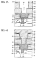
- 4A-4D, 5A, 5B, 6A, and 6B are sectional views of the semiconductor device using the porous insulation film formed of the insulation film forming material according to the present invention as inter-layer insulation films of a multi-interconnection layer structure in the steps of the method for fabricating the semiconductor device, which show the method.
- a gate electrode 12 is formed on a silicon wafer 10.
- Source/drain diffused layer 14a, 14b is formed in the silicon wafer 10 on both sides of the gate electrode 12.
- a transistor including the gate electrode 12 and the source/drain diffused layer 14a, 14b is formed.
- An element isolation film 16 for isolating the transistor is formed on the silicon wafer.
- An inter-layer insulation film 18 and a stopper film 20 are formed in the stated order on the entire surface of the silicon wafer 10 with the thus-formed transistor formed on.
- a contact hole 22 is formed in the inter-layer insulation film 18 and the stopper film 20.
- a titanium nitride film 24 is formed in the contact hole 22, and a conductor plug 26 of tungsten is buried in the contact hole 22.
- a porous insulation film 28 formed of the insulation forming material according to the present invention, and a cap film 30 are formed on the upper surface of the stopper film 20 in the stated order.
- a first interconnection groove 32 of a first interconnection layer pattern, which is connected to the conductor plug 26 is formed in the porous insulation film 28 and the cap film 30.
- a titanium nitride film 34 is formed, and the first interconnection layer 36 of copper is buried.
- a diffusion preventing film 38 of silicon nitride film, a porous insulation film 40 formed of the insulation film forming material according to the present invention, and a diffusion preventing film 42 of silicon nitride film are formed on the upper surface of the cap film 30 in the stated order.
- a via hole 44 is formed in the porous insulation film 40 and the diffusion preventing film 42, connected to the first interconnection layer 36.
- a titanium nitride film 46, and a via layer 48 of copper is buried.
- a porous insulation film 50 formed of the insulation film forming material according to the present invention, and a cap film 52 of silicon nitride film are formed on the upper surface of the diffusion preventing film 42 in the stated order.
- a second interconnection groove 56 of a second interconnection layer pattern, which is connected to the via layer 48 is formed on the porous insulation film 50 and the cap layer 52.
- a titanium nitride film 46 is formed, and a second interconnection layer 60 of copper is buried.
- the inter-layer insulation film 18 and the stopper film 20 are by the usual semiconductor device process in the stated order on the silicon wafer 10 with the transistor including the gate electrode 12, the source/drain diffused layer 14a, 14b, and the element isolation film 16 formed on.
- the contact hole 22 is formed in the inter-layer insulation film 18 and the stopper film 20, connected to the drain diffused layer 14b.
- the titanium nitride film 24 of a 500 nm-thickness is formed in the contact hole 22 by sputtering.
- WF 6 is mixed with hydrogen to be reduced to thereby bury the conductor plug 26 of the tungsten in the contact hole 22.
- the insulation film forming material according to the present invention is applied to the entire surface by spin coating at 3000 rotations for 20 seconds.
- the solvent is dried at 200 °C, and then the silicon wafer is sintered for 30 minutes.
- the porous insulation film 28 is formed in a 450 nm-thickness.
- the cap film 30 is laid on the porous insulation film 28 of a 50 nm-thickness silicon oxide film by CVD using TEOS (TetraEthOxySilane) as a raw material.
- TEOS TetraEthOxySilane
- a resist film 62 for exposing a region for the first interconnection layer pattern to be formed in is formed on the cap film 30 by photolithography.
- the cap film 30 and the porous insulation film 28 are etched by RIE (Reactive Ion Etching) using CF 4 /CHF 3 .
- a 50 nm-thickness titanium nitride film 34 and a 50 nm-thickness seed copper film are formed on the entire surface respectively by sputtering.
- a 600 nm-thickness copper film 64 is formed on the seed copper film by electrolytic plating using the seed copper film as the electrode (FIG. 4C).
- the second interconnection layer 60, and the via layer 48 interconnecting the first interconnection layer 36 and the second interconnection layer 60 are concurrently formed by damascening.
- the diffusion preventing film 38 of a 50 nm-thickness silicon nitride film is formed on the entire surface of the silicon wafer 10 with the first interconnection layer 36 formed on, by plasma CVD using silane and ammonium gas a raw materials.
- a resist film 66 for exposing a region for the via hole 44 to be formed in is formed on the cap film 52 by photolithography.
- the cap film 52, the porous insulation film 50, the diffusion preventing film 42, the porous insulation film 40 and the diffusion preventing film 38 are sequentially etched by RIE using CF 4 /CHF 3 .
- the via hole 44 is formed, connected to the first interconnection layer 36 (FIG. 5B).
- the resist film 66 is removed.
- the cap film 52 and the porous insulation film 50 are sequentially etched by RIE using CF 4 /CHF 3 .
- the second interconnection groove 56 of the second interconnection layer pattern is formed (FIG. 6A).
- the resist film 68 is removed.
- a 50 nm-thickness titanium nitride film 46 and a 50 nm-thickness seed copper film are sequentially formed on the entire surface respectively by sputtering.
- a copper film 70 is formed on the seed copper film in a 600 nm-thickness by electrolytic plating using the seed copper film as the electrode (FIG. 6B).
- the copper film 70, the seed copper film and the titanium nitride film 46 except those in the via hole 44 and the interconnection groove 56 are removed by CMP.
- the porous insulation films 50, 40 of high mechanical strength permit the copper film 70, etc. to be easily removed by CMP.
- the via layer 48 and the second interconnection layer 60 are concurrently formed of the copper film 70 buried in the via hole 44 and the second interconnection groove 56.
- Multi-interconnection layers were formed, for tests, of the insulation film forming material of Example 3 by the above-described semiconductor device fabrication method. A result was that a yield of a million continuous vias was above 90 %.
- Multi-interconnection layers were formed, for tests, of the insulation film forming material of Example 7 by the above-described semiconductor device fabrication method. A result was that a yield of a million continuous vias was above 90 %.
Landscapes
- Chemical & Material Sciences (AREA)
- Chemical Kinetics & Catalysis (AREA)
- Life Sciences & Earth Sciences (AREA)
- Engineering & Computer Science (AREA)
- Materials Engineering (AREA)
- Wood Science & Technology (AREA)
- Organic Chemistry (AREA)
- Internal Circuitry In Semiconductor Integrated Circuit Devices (AREA)
- Formation Of Insulating Films (AREA)
- Compositions Of Macromolecular Compounds (AREA)
- Paints Or Removers (AREA)
- Manufacture Of Porous Articles, And Recovery And Treatment Of Waste Products (AREA)
- Silicon Compounds (AREA)
Abstract
Description

Claims (21)
- An insulation film forming material comprising:a silicon compound having a skeleton of C-C bonds;a porous forming compound which is decomposed or evaporated by a heat treatment; anda solvent which dissolves the silicon compound with the porous forming material.
- An insulation film forming material according to claim 1, wherein
the silicon compound has a structure expressed by the following general formula(Either of R1 and R2 is hydrogen, and the other is hydrocarbon having 1 - 3 carbon atoms or a phenyl group. R3 is hydrocarbon having 1 - 3 carbon atoms or a phenylene group, or oxygen. o is an integer of 20 - 1000.)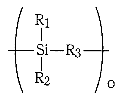
- An insulation film forming material according to claim 1, wherein
the silicon compound has side chains containing hydrogen. - An insulation film forming material according to claim 1, wherein
the silicon compound is one of poly(dimethylcarbosiloxane), poly(hydromethylcarbosilane), poly(diethylcarbosilane), poly(hydroethylcarbosilane), poly(carbosilastyrene), poly(phenylmethylcarbosilane), poly(diphenylcarbosilane), poly(dimethylsilphenylenesiloxane), poly(methylsilphenylenesiloxane), poly(diethylsilphenylenesiloxane), poly(ethylsilphenylene siloxane), poly(dipropylsilphenylenesiloxane), poly(propylsilphenylenesiloxane), poly(phenylsilphenylenesiloxane), poly(phenysilphenylenesiloxane), poly(phenylmethylsilphenylenesiloxane), poly(phenylethylsilphenylenesiloxane), poly(phenylpropylsilphenylenesiloxane), poly(ethylmethylsilphenylenesiloxane), poly(methylpropylsilphenylenesiloxane), and poly(ethylpropylsilphenylenesiloxane). - An insulation film forming material according to claim 1, wherein
the pore forming compound is an amine compound having 4 or more carbon atoms. - An insulation film forming material according to claim 5, wherein
the amine compound is one of aminobutane, diaminobutane, cyclohexylamine, dicyclohexylamine, tetramethylammoniun hydride, hexamethylammonium hydride, and hexadisilylammonium hydride. - An insulation film comprising a film of a silicon compound having a skeleton containing C-C bonds, wherein
pores of below 10 nm-size are formed in the film. - An insulation film according to claim 7, wherein
the silicon compound has a structure expressed by the following general formula(Either of R1 and R2 is hydrogen, and the other is hydrocarbon having 1 - 3 carbon atoms or a phenyl group. R3 is hydrocarbon having 1 - 3 carbon atoms or a phenylene group, or oxygen. o is an integer of 20 - 1000.)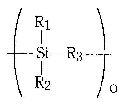
- An insulation film according to claim 7, wherein
the silicon compound is one of poly(dimethylcarbosiloxane), poly(hydromethylcarbosilane), poly(diethylcarbosilane), poly(hydroethylcarbosilane), poly(carbosilastyrene), poly(phenylmethylcarbosilane), poly(diphenylcarbosilane), poly(dimethylsilphenylenesiloxane), poly(methylsilphenylenesiloxane), poly(diethylsilphenylenesiloxane), poly(ethylsilphenylenesiloxane), poly(dipropylsilphenylenesiloxane), poly(propylsilphenylenesiloxane), poly(phenylsilphenylenesiloxane), poly(phenysilphenylenesiloxane), poly(phenylmethylsilphenylenesiloxane), poly(phenylethylsilphenylenesiloxane), poly(phenylpropylsilphenylenesiloxane), poly(ethylmethylsilphenylenesiloxane), poly(methylpropylsilphenylenesiloxane), and poly(ethylpropylsilphenylenesiloxane). - An insulation film according to claim 7, wherein
a ratio of oxygen atom to silicon atom in the skeleton of the film is in the range of 1 silicon atom to 0 - 0.5 oxygen atom. - A method for forming an insulation film comprising the steps of:applying to a substrate an insulation film forming material including a silicon compound having a skeleton containing C-C bonds, a pore forming compound which is decomposed or evaporated by a heat treatment and a solvent which dissolves the silicon compound and the pore forming compound;drying the insulation film forming material applied to the substrate to form a film containing the silicon compound and the pore forming compound; anddecomposing or evaporating the pore forming compound by subjecting the substrate to the heat treatment to eliminate the pore forming compound from the film to form pores in the film.
- A method for forming an insulation film according to claim 11, wherein
the silicon compound has a structure expressed by the following general formula(Either of R1 and R2 is hydrogen, and the other is hydrocarbon having 1 - 3 carbon atoms or a phenyl group. R3 is hydrocarbon having 1 - 3 carbon atoms or a phenylene group, or oxygen. o is an integer of 20 - 1000.)
- A method forming an insulation film accoridng to claim 11, wherein
the silicon compound is one of poly(dimethylcarbosiloxane), poly(hydromethylcarbosilane), poly(diethylcarbosilane), poly(hydroethylcarbosilane), poly(carbosilastyrene), poly(phenylmethylcarbosilane), poly(diphenylcarbosilane), poly(dimethylsilphenylenesiloxane), poly(methylsilphenylenesiloxane), poly(diethylsilphenylenesiloxane), poly(ethylsilphenylenesiloxane), poly(dipropylsilphenylenesiloxane), poly(propylsilphenylenesiloxane), poly(phenylsilphenylenesiloxane), poly(phenysilphenylenesiloxane), poly(phenylmethylsilphenylenesiloxane), poly(phenylethylsilphenylenesiloxane), poly(phenylpropylsilphenylenesiloxane), poly(ethylmethylsilphenylenesiloxane), poly(methylpropylsilphenylenesiloxane), and poly(ethylpropylsilphenylenesiloxane). - A method for forming an insulation film according to claim 11, wherein
a concentration of the pore forming compound in the insulation film forming material is adjusted to thereby control a porosity of the film. - An insulation film forming method according to claim 11, wherein
the pore forming compound is an amine compound containing 4 or more carbon atoms, and
the substrate with the film formed on is subjected to a heat treatment in an atmosphere of a below 5 % oxygen concentration at 300 - 500 °C to form the pores in the film. - A semiconductor device comprising a porous insulation film comprising a film of a silicon compound having a skeleton containing C-C bonds formed on a semiconductor substrate, wherein
pores of below 10 nm-size are formed in the film. - A semiconductor device according to claim 16, further comprising
a buried interconnection layer buried in the porous insulation film. - A semiconductor device according to claim 16, further comprising
a first interconnection layer formed above the semiconductor substrate,
the porous insulation film formed on the first interconnection layer, and
a second interconnection layer formed on the porous insulation film. - A semiconductor device according to claim 16, wherein
the silicon compound has a structure expressed by the following general formula(Either of R1 and R2 is hydrogen, and the other is hydrocarbon having 1 - 3 carbon atoms or a phenyl group. R3 is hydrocarbon having 1 - 3 carbon atoms or a phenylene group, or oxygen. o is an integer of 20 - 1000.)
- A semiconductor device according to claim 16, wherein
the silicon compound is one of poly(dimethylcarbosiloxane), poly(hydromethylcarbosilane), poly(diethylcarbosilane), poly(hydroethylcarbosilane), poly(carbosilastyrene), poly(phenylmethylcarbosilane), poly(diphenylcarbosilane), poly(dimethylsilphenylenesiloxane), poly(methylsilphenylenesiloxane), poly(diethylsilphenylenesiloxane), poly(ethylsilphenylenesiloxane), poly(dipropylsilphenylenesiloxane), poly(propylsilphenylenesiloxane), poly(phenylsilphenylenesiloxane), poly(phenysilphenylenesiloxane), poly(phenylmethylsilphenylenesiloxane), poly(phenylethylsilphenylenesiloxane), poly(phenylpropylsilphenylenesiloxane), poly(ethylmethylsilphenylenesiloxane), poly(methylpropylsilphenylenesiloxane), and poly(ethylpropylsilphenylenesiloxane). - A semiconductor device according to claim 16, wherein
a ratio of oxygen atom to silicon atom in the skeleton of the film of the porous insulation film is in the range of 1 silicon atom to 0 - 0.5 oxygen atom.
Applications Claiming Priority (2)
| Application Number | Priority Date | Filing Date | Title |
|---|---|---|---|
| JP2001338502 | 2001-11-02 | ||
| JP2001338502A JP3886779B2 (en) | 2001-11-02 | 2001-11-02 | Insulating film forming material and insulating film forming method |
Publications (2)
| Publication Number | Publication Date |
|---|---|
| EP1308476A1 true EP1308476A1 (en) | 2003-05-07 |
| EP1308476B1 EP1308476B1 (en) | 2013-08-21 |
Family
ID=19152987
Family Applications (1)
| Application Number | Title | Priority Date | Filing Date |
|---|---|---|---|
| EP02006791.4A Expired - Lifetime EP1308476B1 (en) | 2001-11-02 | 2002-03-25 | Insulation film forming material, insulation film, method for forming the insulation film, and semiconductor device |
Country Status (6)
| Country | Link |
|---|---|
| US (1) | US6727515B2 (en) |
| EP (1) | EP1308476B1 (en) |
| JP (1) | JP3886779B2 (en) |
| KR (1) | KR100777913B1 (en) |
| CN (1) | CN1189927C (en) |
| TW (1) | TWI223851B (en) |
Cited By (2)
| Publication number | Priority date | Publication date | Assignee | Title |
|---|---|---|---|---|
| EP1640404A1 (en) * | 2004-09-22 | 2006-03-29 | JSR Corporation | Polycarbosilane and method of producing the same |
| EP2028215A1 (en) * | 2007-08-10 | 2009-02-25 | Fujitsu Limited | Silicon compound, ultraviolet absorbent, method for manufacturing multilayer wiring device and multilayer wiring device |
Families Citing this family (25)
| Publication number | Priority date | Publication date | Assignee | Title |
|---|---|---|---|---|
| JP4545973B2 (en) * | 2001-03-23 | 2010-09-15 | 富士通株式会社 | Silicon-based composition, low dielectric constant film, semiconductor device, and method of manufacturing low dielectric constant film |
| DE10227615A1 (en) * | 2002-06-20 | 2004-01-15 | Infineon Technologies Ag | Layer arrangement and method for producing a layer arrangement |
| KR100555513B1 (en) * | 2003-08-04 | 2006-03-03 | 삼성전자주식회사 | Metal wiring structure and metal wiring method to prevent voids |
| JP2005175060A (en) * | 2003-12-09 | 2005-06-30 | Jsr Corp | Insulating film, method for forming the same, and film forming composition |
| JP4737361B2 (en) * | 2003-12-19 | 2011-07-27 | Jsr株式会社 | Insulating film and method for forming the same |
| US7256498B2 (en) * | 2004-03-23 | 2007-08-14 | Taiwan Semiconductor Manufacturing Co., Ltd. | Resistance-reduced semiconductor device and methods for fabricating the same |
| JP2005294525A (en) * | 2004-03-31 | 2005-10-20 | Toshiba Corp | Manufacturing method of semiconductor device |
| JP2006002125A (en) * | 2004-06-21 | 2006-01-05 | Tokyo Ohka Kogyo Co Ltd | Film-forming composition comprising carbosilane-based polymer, and film obtained from the composition |
| WO2006009123A1 (en) * | 2004-07-16 | 2006-01-26 | Toagosei Co., Ltd. | Polycarbosilane and method for producing same |
| JP4780277B2 (en) * | 2004-10-15 | 2011-09-28 | Jsr株式会社 | Surface hydrophobizing composition, surface hydrophobizing method, semiconductor device and manufacturing method thereof |
| JP2006152063A (en) * | 2004-11-26 | 2006-06-15 | Jsr Corp | Novel polycarbosilane and method for producing the same, film-forming composition, and film and method for forming the same |
| US7696625B2 (en) * | 2004-11-30 | 2010-04-13 | Semiconductor Energy Laboratory Co., Ltd. | Semiconductor device and method for manufacturing the same |
| US7985677B2 (en) * | 2004-11-30 | 2011-07-26 | Semiconductor Energy Laboratory Co., Ltd. | Method of manufacturing semiconductor device |
| JP2006201361A (en) * | 2005-01-19 | 2006-08-03 | Tokyo Ohka Kogyo Co Ltd | Composition for forming intermediate layer containing silylphenylene polymer and pattern forming method using the same |
| US8368220B2 (en) * | 2005-10-18 | 2013-02-05 | Taiwan Semiconductor Manufacturing Co. Ltd. | Anchored damascene structures |
| JP5321771B2 (en) * | 2005-11-11 | 2013-10-23 | Jsr株式会社 | Method for producing polycarbosilane |
| JP2007131778A (en) * | 2005-11-11 | 2007-05-31 | Jsr Corp | Polycarbosilane, silica-based composition for coating, and silica-based film |
| US8017700B2 (en) | 2005-11-11 | 2011-09-13 | Jsr Corporation | Polycarbosilane, method for producing same, silica composition for coating application, and silica film |
| JP4666308B2 (en) * | 2006-02-24 | 2011-04-06 | 富士通セミコンダクター株式会社 | Manufacturing method of semiconductor device |
| JP2007273494A (en) * | 2006-03-30 | 2007-10-18 | Fujitsu Ltd | Insulating film forming composition and method for manufacturing semiconductor device |
| JP5071474B2 (en) * | 2007-03-13 | 2012-11-14 | 富士通株式会社 | Semiconductor device and manufacturing method of semiconductor device |
| JP5277552B2 (en) * | 2007-03-19 | 2013-08-28 | 富士通セミコンダクター株式会社 | Manufacturing method of semiconductor device |
| JP7048903B2 (en) * | 2017-06-16 | 2022-04-06 | Jsr株式会社 | Silicon-containing film forming composition for pattern forming method and EUV lithography |
| WO2021066574A1 (en) * | 2019-10-02 | 2021-04-08 | 주식회사 엘지화학 | Positive electrode active material for lithium secondary battery and method for preparing positive electrode active material |
| US12610562B2 (en) * | 2022-12-15 | 2026-04-21 | Taiwan Semiconductor Manufacturing Company, Ltd. | Methods of forming bonding structures |
Citations (6)
| Publication number | Priority date | Publication date | Assignee | Title |
|---|---|---|---|---|
| US4870115A (en) * | 1988-03-16 | 1989-09-26 | Shin-Etsu Chemical Co., Ltd. | Foamable silicone rubber composition |
| EP0881668A2 (en) | 1997-05-28 | 1998-12-02 | Dow Corning Toray Silicone Company, Ltd. | Deposition of an electrically insulating thin film with a low dielectric constant |
| US6107357A (en) | 1999-11-16 | 2000-08-22 | International Business Machines Corporatrion | Dielectric compositions and method for their manufacture |
| WO2000075975A2 (en) | 1999-06-07 | 2000-12-14 | Alliedsignal Inc. | Low dielectric constant polyorganosilicon coatings generated from polycarbosilanes |
| US20010033026A1 (en) | 2000-03-29 | 2001-10-25 | Fujitsu Limited | Low dielectric constant film material, film and semiconductor device using such material |
| EP1245628A1 (en) | 2001-03-27 | 2002-10-02 | Samsung Electronics Co., Ltd. | Composition for preparing substances having nano-pores |
Family Cites Families (10)
| Publication number | Priority date | Publication date | Assignee | Title |
|---|---|---|---|---|
| US5470802A (en) * | 1994-05-20 | 1995-11-28 | Texas Instruments Incorporated | Method of making a semiconductor device using a low dielectric constant material |
| US6063714A (en) * | 1995-11-16 | 2000-05-16 | Texas Instruments Incorporated | Nanoporous dielectric thin film surface modification |
| JP3842859B2 (en) | 1997-01-21 | 2006-11-08 | 新日本製鐵株式会社 | Low dielectric constant material, interlayer insulation film and IC substrate |
| US6218318B1 (en) * | 1997-02-05 | 2001-04-17 | Fujitsu Limited | Semiconductor device having a porous insulation film |
| JP3415741B2 (en) | 1997-03-31 | 2003-06-09 | 東レ・ダウコーニング・シリコーン株式会社 | Composition for forming electrically insulating thin film and method for forming electrically insulating thin film |
| JPH1150007A (en) | 1997-08-07 | 1999-02-23 | Catalysts & Chem Ind Co Ltd | Coating liquid for forming low-permittivity silica-based coating film and substrate with coating film |
| JP4528377B2 (en) | 1998-12-25 | 2010-08-18 | 富士通株式会社 | Porous polymer thin film and semiconductor device |
| JP2000273176A (en) | 1999-03-26 | 2000-10-03 | Fujitsu Ltd | Method for forming insulating film and semiconductor device |
| US6204202B1 (en) * | 1999-04-14 | 2001-03-20 | Alliedsignal, Inc. | Low dielectric constant porous films |
| US6602806B1 (en) * | 1999-08-17 | 2003-08-05 | Applied Materials, Inc. | Thermal CVD process for depositing a low dielectric constant carbon-doped silicon oxide film |
-
2001
- 2001-11-02 JP JP2001338502A patent/JP3886779B2/en not_active Expired - Fee Related
-
2002
- 2002-03-22 US US10/102,723 patent/US6727515B2/en not_active Expired - Lifetime
- 2002-03-22 TW TW091105626A patent/TWI223851B/en not_active IP Right Cessation
- 2002-03-25 EP EP02006791.4A patent/EP1308476B1/en not_active Expired - Lifetime
- 2002-04-24 KR KR1020020022411A patent/KR100777913B1/en not_active Expired - Fee Related
- 2002-04-25 CN CNB021184380A patent/CN1189927C/en not_active Expired - Fee Related
Patent Citations (6)
| Publication number | Priority date | Publication date | Assignee | Title |
|---|---|---|---|---|
| US4870115A (en) * | 1988-03-16 | 1989-09-26 | Shin-Etsu Chemical Co., Ltd. | Foamable silicone rubber composition |
| EP0881668A2 (en) | 1997-05-28 | 1998-12-02 | Dow Corning Toray Silicone Company, Ltd. | Deposition of an electrically insulating thin film with a low dielectric constant |
| WO2000075975A2 (en) | 1999-06-07 | 2000-12-14 | Alliedsignal Inc. | Low dielectric constant polyorganosilicon coatings generated from polycarbosilanes |
| US6107357A (en) | 1999-11-16 | 2000-08-22 | International Business Machines Corporatrion | Dielectric compositions and method for their manufacture |
| US20010033026A1 (en) | 2000-03-29 | 2001-10-25 | Fujitsu Limited | Low dielectric constant film material, film and semiconductor device using such material |
| EP1245628A1 (en) | 2001-03-27 | 2002-10-02 | Samsung Electronics Co., Ltd. | Composition for preparing substances having nano-pores |
Cited By (4)
| Publication number | Priority date | Publication date | Assignee | Title |
|---|---|---|---|---|
| EP1640404A1 (en) * | 2004-09-22 | 2006-03-29 | JSR Corporation | Polycarbosilane and method of producing the same |
| US7358317B2 (en) | 2004-09-22 | 2008-04-15 | Jsr Corporation | Polycarbosilane and method of producing the same |
| EP2028215A1 (en) * | 2007-08-10 | 2009-02-25 | Fujitsu Limited | Silicon compound, ultraviolet absorbent, method for manufacturing multilayer wiring device and multilayer wiring device |
| US8207059B2 (en) | 2007-08-10 | 2012-06-26 | Fujitsu Limited | Silicon compound, ultraviolet absorbent, method for manufacturing multilayer wiring device and multilayer wiring device |
Also Published As
| Publication number | Publication date |
|---|---|
| KR100777913B1 (en) | 2007-11-21 |
| US6727515B2 (en) | 2004-04-27 |
| KR20030038308A (en) | 2003-05-16 |
| JP2003142477A (en) | 2003-05-16 |
| JP3886779B2 (en) | 2007-02-28 |
| CN1189927C (en) | 2005-02-16 |
| CN1416158A (en) | 2003-05-07 |
| US20030089903A1 (en) | 2003-05-15 |
| TWI223851B (en) | 2004-11-11 |
| EP1308476B1 (en) | 2013-08-21 |
Similar Documents
| Publication | Publication Date | Title |
|---|---|---|
| US6727515B2 (en) | Insulation film forming material, insulation film, method for forming the insulation film, and semiconductor device | |
| US6780498B2 (en) | Silicon-based composition, low dielectric constant film, semiconductor device, and method for producing low dielectric constant film | |
| US6383907B1 (en) | Process for fabricating a semiconductor device | |
| EP1639635B1 (en) | Methods for forming interconnect structures in integrated circuit devices | |
| US5530293A (en) | Carbon-free hydrogen silsesquioxane with dielectric constant less than 3.2 annealed in hydrogen for integrated circuits | |
| US20010033026A1 (en) | Low dielectric constant film material, film and semiconductor device using such material | |
| WO2002017374A1 (en) | Low-dielectric silicon nitride film and method of forming the same, semiconductor device and fabrication process thereof | |
| US7985700B2 (en) | Composition for forming insulating film and method for fabricating semiconductor device | |
| KR20030026204A (en) | Semiconductor device including porous insulating material and manufacturing method therefor | |
| JP4756526B2 (en) | Method for forming porous low dielectric constant insulating film, porous low dielectric constant insulating film formed by the method, and semiconductor device using the porous low dielectric constant insulating film | |
| US7208405B2 (en) | Insulating film forming method capable of enhancing adhesion of silicon carbide film, etc. and semiconductor device | |
| US20020063312A1 (en) | Plasma induced depletion of fluorine from surfaces of fluorinated low-k dielectric materials | |
| US7875981B2 (en) | Insulating film material, multilayer interconnection structure, method for manufacturing same, and method for manufacturing semiconductor device | |
| US7923820B2 (en) | Method of producing a porous dielectric element and corresponding dielectric element | |
| US20070190461A1 (en) | Material for forming exposure light-blocking film, multilayer interconnection structure and manufacturing method thereof, and semiconductor device | |
| JP2000340557A (en) | Insulating film forming material, insulating film forming method, and semiconductor device | |
| JP2003273098A (en) | Composition for forming low dielectric constant film, low dielectric constant film, method for producing the same, and semiconductor device | |
| JP2003273099A (en) | Composition for forming low dielectric constant film, low dielectric constant film, method for producing the same, and semiconductor device | |
| JP4459096B2 (en) | Manufacturing method of semiconductor device | |
| US20060115980A1 (en) | Method for decreasing a dielectric constant of a low-k film | |
| JP2003243501A (en) | Method for manufacturing semiconductor device | |
| JP3161131B2 (en) | Method for forming insulating film and method for manufacturing semiconductor device | |
| JP2003243384A (en) | Method for manufacturing semiconductor device | |
| JP2004281535A (en) | Film forming material, method of manufacturing insulating film, and semiconductor device | |
| JP2004186593A (en) | Low dielectric constant insulating film, method of manufacturing the same, and semiconductor device |
Legal Events
| Date | Code | Title | Description |
|---|---|---|---|
| PUAI | Public reference made under article 153(3) epc to a published international application that has entered the european phase |
Free format text: ORIGINAL CODE: 0009012 |
|
| AK | Designated contracting states |
Designated state(s): AT BE CH CY DE DK ES FI FR GB GR IE IT LI LU MC NL PT SE TR |
|
| AX | Request for extension of the european patent |
Extension state: AL LT LV MK RO SI |
|
| 17P | Request for examination filed |
Effective date: 20030821 |
|
| AKX | Designation fees paid |
Designated state(s): DE FR GB IT |
|
| 17Q | First examination report despatched |
Effective date: 20050804 |
|
| 17Q | First examination report despatched |
Effective date: 20050804 |
|
| RAP1 | Party data changed (applicant data changed or rights of an application transferred) |
Owner name: FUJITSU MICROELECTRONICS LIMITED |
|
| RAP1 | Party data changed (applicant data changed or rights of an application transferred) |
Owner name: FUJITSU SEMICONDUCTOR LIMITED |
|
| GRAP | Despatch of communication of intention to grant a patent |
Free format text: ORIGINAL CODE: EPIDOSNIGR1 |
|
| GRAS | Grant fee paid |
Free format text: ORIGINAL CODE: EPIDOSNIGR3 |
|
| GRAA | (expected) grant |
Free format text: ORIGINAL CODE: 0009210 |
|
| AK | Designated contracting states |
Kind code of ref document: B1 Designated state(s): DE FR GB IT |
|
| REG | Reference to a national code |
Ref country code: GB Ref legal event code: FG4D |
|
| REG | Reference to a national code |
Ref country code: DE Ref legal event code: R096 Ref document number: 60245391 Country of ref document: DE Effective date: 20131017 |
|
| PG25 | Lapsed in a contracting state [announced via postgrant information from national office to epo] |
Ref country code: IT Free format text: LAPSE BECAUSE OF FAILURE TO SUBMIT A TRANSLATION OF THE DESCRIPTION OR TO PAY THE FEE WITHIN THE PRESCRIBED TIME-LIMIT Effective date: 20130821 |
|
| PLBE | No opposition filed within time limit |
Free format text: ORIGINAL CODE: 0009261 |
|
| STAA | Information on the status of an ep patent application or granted ep patent |
Free format text: STATUS: NO OPPOSITION FILED WITHIN TIME LIMIT |
|
| 26N | No opposition filed |
Effective date: 20140522 |
|
| REG | Reference to a national code |
Ref country code: DE Ref legal event code: R097 Ref document number: 60245391 Country of ref document: DE Effective date: 20140522 |
|
| GBPC | Gb: european patent ceased through non-payment of renewal fee |
Effective date: 20140325 |
|
| REG | Reference to a national code |
Ref country code: FR Ref legal event code: ST Effective date: 20141128 |
|
| PG25 | Lapsed in a contracting state [announced via postgrant information from national office to epo] |
Ref country code: GB Free format text: LAPSE BECAUSE OF NON-PAYMENT OF DUE FEES Effective date: 20140325 Ref country code: FR Free format text: LAPSE BECAUSE OF NON-PAYMENT OF DUE FEES Effective date: 20140331 |
|
| PGFP | Annual fee paid to national office [announced via postgrant information from national office to epo] |
Ref country code: DE Payment date: 20170321 Year of fee payment: 16 |
|
| REG | Reference to a national code |
Ref country code: DE Ref legal event code: R119 Ref document number: 60245391 Country of ref document: DE |
|
| PG25 | Lapsed in a contracting state [announced via postgrant information from national office to epo] |
Ref country code: DE Free format text: LAPSE BECAUSE OF NON-PAYMENT OF DUE FEES Effective date: 20181002 |