The present invention relates to image
processing apparatuses and image scanning apparatuses
such as monochrome copiers, color copiers, facsimiles
and scanners and, more particularly, to an image
processing apparatus and an image scanning apparatus
capable of detecting and correcting an abnormal pixel
showing up as a white streak and a black streak on an
image caused by dust when a sheet-through document
feeder (SDF) is used.
In conventional image scanning apparatuses
such as copiers, a scanned image is adversely influenced
by dust on a base board or a contact glass, thereby
deteriorating an image produced from the scanned image.
Japanese Laid-Open Patent Application No. 11-112800
discloses an image scanning apparatus to address
the above-mentioned problem. The image scanning
apparatus stores pixel data read from a base board of
the image scanning apparatus. Based on the read pixel
data, the image scanning apparatus detects an abnormal
pixel whose output value exceeds those of adjacent
pixels above a predetermined value. Then, the image
scanning apparatus corrects the output value of the
detected abnormal pixel by using the output values of
the adjacent pixels and replaces the output value of the
abnormal pixel with the corrected one.
In addition, in Japanese Laid-Open Patent
Application No. 2000-196881, an image scanning apparatus
optimizes SDF-based correction and platen-based
correction separately, whereby enabling a copier to
produce an image optimally as well as a facsimile to
produce a binary image optimally.
In Japanese Laid-Open Patent Application No.
10-294870, an image scanning apparatus divides a white-based
range into a plurality of blocks in the sub-scan
direction. For each of the blocks, the image scanning
apparatus computes an average of values read from pixels
in the block. Comparing the computed averages of the
blocks, the image scanning apparatus identifies and
eliminates a block suffering from dust in order to set a
white basis from the remaining blocks.
However, any of the above-mentioned image
scanning apparatuses use density information on pixels
adjacent in the main-scan direction to correct a pixel
suffering from dust. As a result, the image scanning
apparatuses have a disadvantage that there may be a lack
of pixel continuity related to a corrected range in the
sub-scan direction when the image scanning apparatuses
deal with an image having a strong correlation related
to the sub-scan direction.
In addition, vibration of the SDF may result
in fluctuation of a position to be read, thereby
interfering with reliable detection of an abnormal pixel.
Under this situation, since the abnormal pixel is
corrected unsuccessfully for the sake of fluctuation of
the correction, an improper portion of an image such as
a white streak or a black streak may remain in a
produced image.
It is a general object of the present
invention to provide an improved and useful image
processing apparatus and an improved and useful image
scanning apparatus in which the above-mentioned problems
are eliminated.
A more specific object of the present
invention is to provide an image processing apparatus
and an image scanning apparatus capable of detecting
accurately a position of a pixel whose image information
is lost because of obstruction of dust toward reflected
light and correcting properly the detected pixel without
impairing the pixel continuity in the sub-scan direction
with reference to normal pixels in the neighborhood of
the detected pixel.
In order to achieve the above-mentioned
objects, there is provided according to one aspect of
the present invention an image processing apparatus for
processing image data read from a manuscript by an image
scanning apparatus illuminating light from an illuminant
to the manuscript that is delivered by a manuscript
delivery part and receiving reflected light from a
surface of the manuscript by a photoelectric converting
part to convert into digital data, comprising: an
abnormal pixel detecting part moving the image scanning
apparatus by a predetermined small distance to read a
null-image part before the image scanning apparatus
reads the manuscript and detecting an abnormal pixel
from a plurality of lines in image data read from the
null-image part; and an abnormal pixel correcting part
correcting an abnormal pixel in the image data read from
the manuscript by the image scanning apparatus on the
basis of information on the abnormal pixel detected by
the abnormal pixel detecting part.
According to the above-mentioned invention, it
is possible to detect accurately an abnormal pixel
caused by dust and others by weakening influence on
noise and correct successfully a vertical streak
resulting from the abnormal pixel. As a result, the
image processing apparatus can read a high-quality image
with high reliability.
In the above-mentioned image processing
apparatus, the image processing apparatus may further
comprise a white back board at a position where light is
illuminated from the illuminant of the image scanning
apparatus, wherein the abnormal pixel detecting part
checks whether or not there is black dust on glass that
obstructs the reflected light on the basis of
information on image data read from the white back board
before said manuscript is delivered.
In the above-mentioned image processing
apparatus, the image processing apparatus may further
comprise a black back board at a position where light is
illuminated from the illuminant of the image scanning
apparatus, wherein the abnormal pixel detecting part
checks whether or not there is white dust on glass that
obstructs the reflected light on the basis of
information on image data read from the black back board
before the manuscript is delivered.
In the above-mentioned image processing
apparatus, the image processing apparatus may further
comprise a back board having a white back board and a
black back board at a position where light is
illuminated from the illuminant of the image scanning
apparatus, wherein the abnormal pixel detecting part
checks whether or not there are black dust and white
dust on glass that obstructs the reflected light on the
basis of information on image data read from the white
back board and the black back board in a manner in which
the back board slides or rotates to switch the white
back board and said black back board alternately before
the manuscript is delivered.
According to the above-mentioned invention, it
is possible to detect accurately the position of an
abnormal pixel caused by a black object such as dust or
a white object such as paper dust lying on a glass.
In the above-mentioned image processing
apparatus, the abnormal pixel detecting part may conduct
two-dimensional search for a candidate of abnormal
pixels in the image data from a plurality of lines in
the image data read from the null-image part and detect
a maximal range of a one-dimensional projection while
the image scanning part is still at a predetermined
position.
According to the above-mentioned invention, it
is possible to identify a boundary of dust and others
through the two-dimensional search and detect an
appropriate range of pixels where correction should be
performed. At the same time, it is also possible to
gain an average density of abnormal pixels.
In the above-mentioned image processing
apparatus, the abnormal pixel detecting part may take an
average in the sub-scan direction of a plurality of
lines in the image data read from the null-image part,
binarize an averaged image data to detect an abnormal
pixel, and take an average in the main-scan direction of
the averaged image data in the sub-scan direction to
compute a density of the abnormal pixel.
According to the above-mentioned invention, it
is possible to gain accurately a position of an abnormal
pixel and a density of the abnormal pixel.
In the above-mentioned image processing
apparatus, the abnormal pixel correcting part may have
an abnormal pixel deleting part for deleting a range
including an abnormal pixel detected by the abnormal
pixel detecting part from image data read by the image
scanning apparatus on the basis of information on a
position of the abnormal pixel and a pixel enlarging
part for enlarging a length of a deleted image data to a
length of the image data read by the image scanning
apparatus.
According to the above-mentioned invention, it
is possible to produce an image without a vertical
streak caused by an abnormal pixel.
In the above-mentioned image processing
apparatus, the abnormal pixel correcting part may have a
density correcting part for decreasing a density of
pixels in a range including an abnormal pixel detected
by the abnormal pixel detecting part from image data
read by the image scanning apparatus on the basis of
information on a position of the abnormal pixel and a
density of the abnormal pixel and an MTF weak-correcting
part for weakening MTF correction for pixels in the
range including an abnormal pixel detected by the
abnormal pixel detecting part from image data read by
the image scanning apparatus.
According to the above-mentioned invention,
the abnormal pixel correcting part decrease a density of
pixels within a range where a vertical streak may appear
under influence of an abnormal pixel to gain normal
pixels.
In the above-mentioned image processing
apparatus, the abnormal pixel correcting part may have a
surrounding pixel statistic operating part for producing
correction data from pixels around a range including an
abnormal pixel detected by the abnormal pixel detecting
part from image data read by the image scanning
apparatus on the basis of information on a position of
the abnormal pixel and a data switching part for
substituting a pixel that is anticipated to become
abnormal for the correction data.
According to the above-mentioned invention,
the abnormal pixel correcting part can considerably
decrease a vertical streak.
In the above-mentioned image processing
apparatus, the abnormal pixel correcting part may have a
surrounding pixel variance computing part for
constructing a pixel matrix whose center element is the
abnormal pixel and computing an average of surrounding
pixels in a direction whose variance is less than any
other direction with reference to normal pixels in each
direction of the matrix in order to substitute the
abnormal pixel for the average.
In the above-mentioned image processing
apparatus, the abnormal pixel correcting part may have
an average computing part for constructing a pixel
matrix whose center element is the abnormal pixel and
computing an average of only normal surrounding pixels
in order to substitute the abnormal pixel for the
average.
In the above-mentioned image processing
apparatus, the abnormal pixel correcting part may have a
maximum detecting part for constructing a pixel matrix
whose center element is the abnormal pixel and detecting
a pixel with a maximal density in a left-side column of
the matrix and a pixel with a maximal density in a
right-side column of the matrix and an average computing
part for correcting the abnormal pixel by using the
pixel with a maximal density in a left-side column of
the matrix and the pixel with a maximal density in a
right-side column of the matrix.
In the above-mentioned image processing
apparatus, the abnormal pixel correcting part has a
binarization/measurement processing part for
constructing a pixel matrix whose center element is the
abnormal pixel and binarizing pixels in the matrix
surrounding the center element and a dynamic average
computing part for producing correction data on the
basis of a proportion of numbers of "0" and "1" in
binarized data.
According to the above-mentioned invention,
the abnormal pixel correcting part can conduct
appropriate correction without a loss of continuity of
an image in the sub-scan direction, thereby reading a
high-quality image with high reliability.
In the above-mentioned image processing
apparatus, the abnormal pixel correcting part may have a
surrounding pixel computing part for constructing a
pixel matrix whose center element is the abnormal pixel
and computing an average of surrounding pixels in a
direction whose variance is less than any other
direction with reference to normal pixels in each
direction of the matrix in order to substitute the
abnormal pixel for the average, an average computing
part for computing an average of only normal surrounding
pixels in order to substitute the abnormal pixel for the
average, and a data switching part for select either
correction data substituted by the surrounding pixel
computing part or correction data substituted by the
average computing part according to a mode setting of an
image.
According to the above-mentioned invention,
the abnormal pixel correcting part can conduct optimal
correction according to a type of manuscript and read a
high-quality image with high reliability.
In the above-mentioned image processing
apparatus, the image processing apparatus further may
comprise an image displaying part for displaying a
corrected image.
According to the above-mentioned invention, an
operator can check whether or not the correction is
successful with reference to a displayed image and
determine whether the correction will be valid hereafter
or a condition of the correction should be altered. As
a result, the abnormal pixel correcting part can conduct
optimal correction according to a type of manuscript and
read a high-quality image with high reliability.
Additionally, there is provided according to
another aspect of the present invention an image
scanning apparatus for illuminating light from an
illuminant to a manuscript that is delivered by a
manuscript delivery part and receiving reflected light
from a surface of the manuscript by a photoelectric
converting part to convert into digital data,
comprising: an abnormal pixel detecting part detecting a
position of an abnormal pixel from which information
data cannot be read due to a black object such as dust
and a white object such as paper dust lying on a glass
between the manuscript and the photoelectric converting
part before a portion of reflected light from a surface
of the manuscript is reached to the photoelectric
converting part; and a cleaning alarming part supplying
an alarm to urge cleaning on the glass when the abnormal
pixel detecting part detects an abnormal pixel.
Additionally, there is provided according to
another aspect of the present invention an image
scanning apparatus for illuminating light from an
illuminant to a manuscript that is delivered by a
manuscript delivery part and receiving reflected light
from a surface of the manuscript by a photoelectric
converting part to convert into digital data,
comprising: an abnormal pixel detecting part detecting a
position of an abnormal pixel from which information
data cannot be read due to a black object such as dust
and a white object such as paper dust lying on a glass
between the manuscript and the photoelectric converting
part before a portion of reflected light from a surface
of the manuscript is reached to the photoelectric
converting part; and a cleaning part cleaning a surface
of the glass when the abnormal pixel detecting part
detects an abnormal pixel.
According to the above-mentioned invention, it
is possible to prevent a lack of image information and
to read a high-quality image with high reliability.
Other objects, features and advantages of the
present invention will become more apparent from the
following detailed description when read in conjunction
with the accompanying drawings.
An embodiment of the present invention will
now be described with reference to figures.
FIG. 1 is a diagram illustrating a structure
of an image scanning apparatus. The image scanning
apparatus comprises a reading part 1, a manuscript
carrying part 2 and a manuscript reading platform 3.
The reading part 1 includes an optical system for
exposure scanning 9 comprising a first scanning part 4,
a second scanning part 5, a lens 6, a one-dimensional
photoelectric converting element such as a CCD 7 and a
stepping motor 8 for driving the first scanning part 4
and the second scanning part 5. Furthermore, the first
scanning part 4 comprises an illuminant 4a formed of a
xenon lamp or a fluorescent lamp and a mirror 4b, and
the second scanning part 5 comprises mirrors 5a and 5b.
The manuscript carrying part 2 comprises a sheet-through
document feeder (SDF) 10 and a manuscript platform 11.
The SDF 10 has a stepping motor 12. A manuscript press
board 14 for pressing a manuscript is equipped over the
manuscript reading platform 3. The manuscript press
board 14 is capable of rotating freely. A white
reference board 15 for shading correction is placed at
an edge of the manuscript reading platform 3.
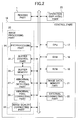
FIG. 2 is a block diagram illustrating a
structure of a control part of the image scanning
apparatus in FIG. 1. As shown in the block diagram in
FIG. 2, the control part 16 comprises a CPU 17
administrating entire operations in the image scanning
apparatus, a RAM 18 serving as a working memory for the
CPU 17, a ROM 19 storing some control programs, an image
processing part 20, an image data memory part 21 and an
external connecting part 22 controlling a delivery of
data stored in the image data memory part 21 to an
external apparatus such as a computer. The control part
16 is connected with the reading part 1 and an operation
displaying part 23. The image processing part 20
comprises a preprocessing part 24, a buffer control part
25, a buffer memory 26, an abnormal pixel detecting part
27, an abnormal pixel correcting part 28 and an image
quality correcting part 29.
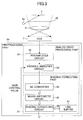
FIG. 3 is a block diagram illustrating a
structure of the preprocessing part 24 in FIG. 2. As
shown in the block diagram in FIG. 3, the preprocessing
part 24 comprises an analog video processing part 30 and
a shading correcting part 31. The analog video
processing part 30 has a preamplifier circuit 32 and a
variable amplifier circuit 33. The shading correcting
part 31 has an A/D converter 34, a black arithmetic
circuit 35, a shading correcting circuit 36 and a line
buffer 37. The illuminant 4a illuminates light to the
manuscript 13 on the manuscript platform 3. Through a
shading adjusting board 38, the reflected light from the
manuscript 13 is gathered by the lens 6, which is sent
to the CCD 7. The shading adjusting board 38 is
responsible to adjust an amount of light so that a
center and an edge of the CCD 7 can have the same amount
of light. At execution of the shading correction, when
there is much difference in the amount of light between
the center and the edge of the CCD 7, the correction
results in distortion. Accordingly, after eliminating
the difference in the amount of light in advance as the
above-mentioned manner, the shading correction should be
performed.
A description will now be given, with
reference to FIG. 4 and FIG. 5, of two manuscript
reading modes of the image scanning apparatus: a book
mode and an SDF mode. In the book mode, the image
scanning apparatus puts the manuscript 13 on the
manuscript reading platform 3 to read image data of the
manuscript 13 as shown in FIG. 4. In the SDF mode, the
image scanning apparatus reads the image data of the
manuscript 13 while the manuscript carrying part 2
carries the manuscript 13 as shown in FIG. 5.
Under the book mode, the image scanning
apparatus mainly performs as follows: After the
manuscript 13 is set on the manuscript reading platform
3 beneath the manuscript press board 14, the CPU 17
powers the illuminant 4a on. Next, the CCD 7 reads the
white reference board 15, and the A/D converter 34 of
the preprocessing part 24 performs analog to digital
conversion for image data read from the white reference
board 15. The digital image data is maintained as
reference data for the shading correction. Then, the
CPU 17 lets the first scanning part 4 moving to a
position of the manuscript 13. The first scanning part
4 scans a surface of the manuscript 13 while moving at a
constant speed. At the time, the CCD 7 performs
photoelectric conversion for an image of the manuscript
13 and sends the resulting image data as an analog video
signal to the preprocessing part 24 of the image
processing part 20.
After the analog video signal to the
preprocessing part 24 is amplified in the analog video
processing part 30, the amplified analog video signal is
converted into a digital signal in the A/D converter 34
of the shading correcting part 31. Under a gain
adjustment of the A/D conversion, a black level
adjustment and a white level adjustment are performed in
order to assure a dynamic range of the digital signal.
When the read image data is mainly formed of
characters, the distinction between the characters and
background of the manuscript 13 can be clearly
recognized. In this situation, if the background
contains dust, signal levels corresponding to the dust
are removed. On the other hand, when the read image
data is formed of a picture, it is necessary to prepare
a wide range of gradation. In this situation, the
background of the manuscript 13 should not be removed
because the background may contain important information.
In addition, it is possible to change a level of
quantization together with a pixel density of the read
image depending on a size of the read image data and how
an external device connected with the image scanning
apparatus uses the read image data. For example, when
an artistic image such as a graphic art is read, it is
expected to enhance resolution and the level of
quantization per a pixel. On the other hand, when
character information is extracted from an image that is
created for optical character reader (OCR), coarse
resolution and the lower level of quantization is
sufficient.
For the resulting digital image data, the
shading correction and spectral unevenness are performed
to correct spectral distribution of the illumination
system, and some image data processes are performed for
the resulting digital image data.
If the digital image data is expected to be
used as binary data, the corresponding binary data is
created. If the digital image data is expected to be
used as multi-valued data, the corresponding 8-bit data
is created. The created data is stored in the image
data memory part 21 and is delivered to a host computer
and others through the external connecting part 22.
Under the SDF mode, the image scanning
apparatus mainly performs as follows: At the beginning,
the image scanning apparatus reads the white reference
board 15. As shown in FIG. 5, a detaching roller 39
detaches a sheet of the manuscript 13 on the manuscript
platform 11 one by one. A carrying roller 40 carries
the detached sheet of the manuscript 13 to a
predetermined position where the first scanning part 4
reads an image of the sheet. At this time, the
manuscript 13 is being carried at a constant speed so
that the first scanning part 4 can read the image of the
manuscript 13 through the CCD 7 in a stationary state.
Subsequent processes are performed similarly to those
under the book mode. The resulting image data is stored
in the image data memory part 21 as binary data or
multi-valued data.
The detailed description will now be given,
with reference to FIG. 6, of actions for reading an
image of the manuscript 13 under the SDF mode. As
mentioned above, in order to read the image of the
manuscript 13 that is carried at a constant speed, the
first scanning part 4 is fixed at the predetermined
position. The read image is formed as a mirror image of
the corresponding image obtained under the book mode
related to the main-scan direction. Consequently, when
the read image is output, it is necessary to perform a
mirroring process whereby the right and the left of the
read image are exchanged. A stepping motor controls how
the manuscript 13 is carried. When the read image is
scaled up or down related to the direction where the
manuscript 13 is being carried (the sub-scan direction),
the stepping motor changes the moving speed of the
manuscript 13.
A sequence of actions for the above-mentioned
operation is as follows; The first scanning part 4 is
staying at its home position 41, where the first
scanning part 4 scans an image of the manuscript 13.
Before reading the image, the first scanning part 4
needs to read the white reference board 15 for the
shading correction. In order to read the white
reference board 15, the first scanning part 4 being now
at the home position 41 temporally moves beneath the
white reference board 15. Then, the first scanning part
4 reads illumination distribution of the white reference
board 15 and produces shading data to normalize read
data. Then, the first scanning part 4 moves back to the
home position 41. The first scanning part 4 is fixed at
the home position 41 to read the image of the carried
manuscript 13. The manuscript 13 is thrown in a
manuscript input part 42, is carried through beneath the
home position 41 and is thrown out a manuscript output
part 43. When the manuscript 13 is carried through
beneath the home position 41, the first scanning part 4
reads the manuscript 13. At this time, if there is any
black dust on a surface of a contact glass, the read
image ends up an image with a black streak 45 shown in
FIG. 7. On the other hand, if there is any dust on the
surface of the contact glass, the read image ends up an
image with a white streak 46 shown in FIG. 7.
In order to detect an abnormal pixel caused by
the dust, as soon as the first scanning part 4 returns
at the home position 41, the first scanning part 4 reads
the surface of the contact glass in a state without any
image by illuminating light from the illuminant 4a.
Basically, the first scanning part 4 reads a condition
of a back board 44 of the SDF 10 for pressing the
carried manuscript 13. In order to detect an abnormal
pixel caused by black dust on the contact glass, a back
board 44 should be white-colored. If there is no black
dust on the contact glass, the first scanning part 4
results in reading a white image. On the other hand, in
order to detect an abnormal pixel caused by white dust
on the contact glass, the back board 44 should be black-colored.
If there is no white dust on the contact glass,
the first scanning part 4 results in reading a black
image. Incorporating the above-mentioned properties,
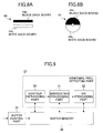
two types of the back board 44 are presented in FIG. 8A
and FIG. 8B. As shown in FIG. 8A, the back board 44 may
be formed of a black back board 44a and a white back
board 44b so that the back board 44 can slide to switch
the colors. As shown in FIG. 8B, the back board 44 may
be shaped as a cylinder one half of which is formed of
the black back board 44a and the other half of which is
formed of the white back board 44b. Rotation of the
back board 44 switches the colors.
The abnormal pixel detecting part 27 of the
image processing part 20 is responsible to detect an
abnormal pixel caused by dust on the contact glass. As
shown in FIG. 9, the abnormal pixel detecting part 27
comprises a contour emphasizing part 50, a binarization
processing part 51 and an OR processing part 52. The
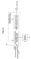
abnormal pixel correcting part 28 is responsible to
correct the detected abnormal pixel on the basis of
image information on the abnormal pixel stored in the
buffer memory 26 when the manuscript 13 is read. As
shown in FIG. 10, the abnormal pixel correcting part 28
comprises a main-scan direction abnormal pixel deleting
part 53 and a main-scan direction pixel enlarging part
54. Based on the corrected image data, the image
quality correcting part 29 enhances the corrected image
data by using a variety of image processing techniques
in accordance with a quality required by an external
device connected with the external connecting part 22:
an error diffusing process, a dither process, a
binarization process, a density conversion, a white-black
inversion, a filtering process, a variable power
process and a image shifting process. The resulting
image data is stored in the image data memory part 21
and is delivered to the external device through the
external connecting part 22. Operations executed in the
image quality correcting part 29 are determined in
accordance with the request of the external device.
Thus, no image quality enhancing operation may be
executed in the image quality correcting part 29. For
example, if all image quality enhancing operation are
executed in the external device, only the abnormal pixel
correcting process is executed without executing any
image quality enhancing operation in the image quality
correcting part 29. In this case, the resulting image
data is stored in the image data memory part 21 as an
original image data.
A description will now be given, with
reference to a flowchart in FIG. 11, of actions at the
time when image data of the manuscript 13 is read under
the SDF mode of the image scanning apparatus mentioned
above.
In order to read the white reference board 15,
the first scanning part 4 now being in the home position
41 temporally moves beneath the white reference board 15,
reads illumination distribution of the white reference
board 15 and produces shading data to normalize read
data. After those tasks, the first scanning part 4
returns to the home position (step S1) Soon after the
first scanning part 4 returns, the illuminant 4a
illuminates light in a state without any image to read a
surface of a contact glass, that is, the back board 44.
When the first scanning part 4 reads the back board 44,
the image scanning apparatus lets the first scanning
part 4 not fixed at the home position 41 but scan a
plurality of lines in the sub-scan direction. Then, the
image scanning apparatus stores the read data in the
buffer memory 26 (step S2). At the storage of the read
data in the buffer memory, the buffer control part 25
does not have to maintain the whole image data. It is
sufficient to store just a range of image where the
image scanning apparatus can detect dust in order to use
efficiently an occupied amount of the memory.
FIG. 12A illustrates a level of an electrical
output of the read image in the main-scan direction in a
case that the back board 44 is white when the image is
read. In the case, a white range of the image has a
high level of the electrical output, whereas a black
range of the image has a low level of the electrical
output. If there is no abnormal pixel caused by dust,
the level of the electrical output would become constant
at the high level of the white range except both edges
of the electrical output. If there are some abnormal
pixels caused by dust, the range where the abnormal
pixels are lying would have the low level of the black
range. FIG. 12B illustrates a case that there are some
abnormal pixels. As shown in FIG. 12B, if dust 55 is in
some places, the dust 55 can give some influence to
other pixels on a plurality of lines in which the dust
55 is read because the dust 55 occupies an area for
itself. As illustrated in FIG. 12B, suppose that the
dust 55 is lying in a plurality of lines from a first
line to a third line and the first scanning part 4 is
currently located at a second line where the first
scanning part 4 should be located at the reading of the
image in a stationary state. In this case, if a
position of the line where the first scanning part 4
reads the image fluctuates for some reasons, a position
of the dust 55 is also changed slightly. FIG. 12C
illustrates an average density obtained when the dust 55
lying in the range from the first line to the third line
is projected in the vertical direction. In order to
detect accurately an abnormal pixel caused by the dust
55 that occupies a plurality of the lines, the first
scanning part 4 additionally scans a plurality of the
lines in the sub-scan direction as well as the main-scan
direction. There are some reasons that a position in
which the first scanning part 4 reads the image
fluctuates slightly. Since the first scanning part 4
moves mechanically to a predetermined position, the
first scanning part 4 may move to a position different
slightly from a predetermined position for the sake of
vibration resulting from the manuscript feeding. In
addition, some dust on the surface is also likely to
move around for the sake of the vibration and airflow
while the image of the manuscript 13 is read. In order
to overcome the trouble, the first scanning part 4 scans
a plurality of the lines in the sub-scan direction,
thereby also preventing a noise signal caused by the
vibration and other factors.
The abnormal pixel detecting part 27 detects
an abnormal pixel in image data that has been read in
the state without any image by the first scanning part 4
and has been stored in the buffer memory 26 (step S3).
In order to detect the abnormal pixel in the image data
stored in the buffer memory 26, the contour emphasizing
part 50 executes a two-dimensional filtering process by
using a filter 56 as shown in FIG. 13A and emphasizes
edges of the abnormal pixel to define a boundary of the
area occupied by dust 55 so that the abnormal pixel
detecting part 27 can use the two-dimensional image
stored in the buffer memory 26 to determine
appropriately what extent of pixels the abnormal pixel
gives influence. Then, a binarization processing part
51 performs binarization for the resulting contour
emphasized image on the basis of a predetermined
threshold to discriminate between the abnormal pixel and
a normal pixel. In addition, an OR processing part 52
performs an OR process for the resulting binarized image
data with respect to each of the positions read in the
main-scan direction by the first scanning part 4.
Namely, for a normal pixel not being in the first line,
a fluctuation of a position where the image is read in
the sub-scan direction may make the normal pixel
abnormal under the influence of the first line.
Therefore, the OR processing part 52 performs the OR
process for a whole range where the abnormal pixel may
emerge so that the abnormal pixel detecting part 27 can
consider all pixels in the whole range to be candidates
of abnormal pixels. Then, the resulting candidates are
related to coordinates in the main-scan direction and
are stored in the buffer memory 26. FIG. 13B
illustrates data containing abnormal pixels 57 that is
stored in the buffer memory 26. In the data 57 shown in
FIG. 13B, a position having "0" means that a pixel at
the position is normal, and a position having "1" means
that a pixel at the position is likely to become
abnormal.
After detecting the abnormal pixel, the image
scanning apparatus is ready to read the manuscript 13
(step S4). The image data read from the manuscript 13
includes not only image data of the manuscript 13 itself
but also information on the dust 55. The abnormal pixel
correcting part 28 uses information of an abnormal pixel
caused by the dust 55 to remove information of the dust
55 from the read image data and correct the abnormal
pixel of the read image data (step 5). Actually, a
main-scan direction abnormal pixel deleting part 53 of
the abnormal pixel correcting part 28 is responsible to
delete the abnormal pixel in the main-scan direction
from the image data read from the manuscript 13 with
reference to the information on the abnormal pixel
caused by the dust 55 in the buffer memory 26. This
deletion of the abnormal pixel results in shortening the
length of the image data of the manuscript 13 in the
main-scan direction. In order to restore the original
image data of the manuscript 13, a main-scan direction
pixel enlarging part 54 is responsible to enlarge the
image data without any abnormal pixels in compensation
for the deleted portion of the image data. This
enlarging process exploits a resampling process for
scaling up and down image data.
The resampling process will now be described.
In a scaling process of image data, required data is
interpolated by resampling a sampling signal. A
convolution operation is preformed for the digital
sampling signal. By applying a sampling function h(r)
in FIG. 14A for the digital sampling signal, the
convolution operation can completely restore a
continuous signal corresponding to the digital sampling
signal. In a scaling-up process, more sampling points
are required to restore data. In a scaling-down process,
by contrast, sampling points are decreased by
lengthening intervals between sampling points. Although
the sampling point r for digital data has a discrete
value, it is not necessary that the sampling point r is
an integer. Let input digital data be f(r) and
resampling data g(r). The g(r) is computed as follows;
g(r) = f(r)*h(r), where a notation "*" represents the
convolution operation summing all products of the
sampling point r and each of points adjacent to the
sampling point r.
There are some approximation methods for
generating interpolation data except the computation
based on the sampling function h. Especially, some
approximation formulae such as the nearest pixel
substitution method, the method of distance linear
distribution between adjacent pixels and the method of
three-dimensional function convolution operation related
to the sampling function are often used for the sake of
some constraints related to hardware configuration in
use. The nearest pixel substitution method substitutes
a resampling point for original input data nearest to a
resampling point. The method of distance linear
distribution between adjacent pixels assigns a density
according to distances between a resampling point and
each of the adjacent pixels. The method of three-dimensional
function convolution operation approximates
a sampling function based on a trigonometric function to
a three-dimensional function. The resulting three-dimensional
function is used to compute interpolation
when densities of pixels adjacent to a resampling point
are distributed to assign a density of the resampling
point. Since these approximation methods aims at
implementation in hardware, an appropriate method should
be selected on the basis of a tradeoff between required
image quality and resources required to implement the
method on the hardware.
FIG. 14B illustrates interpolation for
resampling positions. When a processor and a controller
are used to perform the interpolation, any constraint of
hardware configuration to the above-mentioned
approximation can be ignored. Although there still
remains a constraint on a tradeoff between time and a
degree of approximation, the degree of approximation is
improved under programmable configuration. In FIG. 14B,
white circles represent original image data, and a
density of a position j is notated as a S(j). Also, a
white triangle represents interpolation data E(k) at a
resampling point k.
The main-scan direction enlarging part 54
supplies a resampling position to perform the scaling-up
process and executes the convolution operation for the
resampling position. When the computation is performed
by a programmable processor, the computation for the
above-mentioned resampling process can be performed with
high precision because of no constraint on the hardware
in use.
A description will now be given, with
reference to FIG. 15, of a sequence of processes for the
abnormal pixel correcting part 28 to delete abnormal
pixels in the image data of the manuscript 13 and then
enlarge the resulting image data. FIG. 15-(a)
illustrates data containing abnormal pixels 57 that have
been detected in the abnormal pixel detecting part 27
and stored in the buffer memory 26. In FIG. 15-(a), a
position containing "0" means that a pixel at the
position is normal, and a position containing "1" means
that a pixel at the position is likely to become
abnormal. Image data 58 in FIG. 15-(b) is formed of a
line of pixels in the sub-scan direction that is
extracted from image data of the manuscript 13. Pixels
corresponding to two positions with "1" show up as
images with a black streak 59. In FIG. 15-(c), image
data 60 results from deletion of the two pixels in the
main-scan direction causing the images with the black
streak 59. When the images with the black streak 59 are
deleted, the main-scan direction abnormal pixel deleting
part 53 actually skips the reading of the two positions
corresponding to abnormal pixels at access to a sequence
of pixel data 57. After skipping, the main-scan
direction abnormal pixel deleting part 53 subsequently
starts to read a position of the next normal pixel in
the sequence of pixel data 57, thereby deleting the
abnormal pixels from the image data containing the two
abnormal pixels. Then, the main-scan direction pixel
enlarging part 54 enlarges the resulting image data 60
just enough long to supply an enlarged image data 61 of
a predetermined length. In this scaling-up process,
there are two methods to interpolate a deleted portion.
One method interpolates the deleted portion by using the
whole remaining image data. The other method
interpolates the deleted portion by using pixels of the
remaining image data that are in the neighborhood of the
deleted portion. If interpolated by the former method,
resampling information prevails to the whole range of
the image, whereby an inherent vertical streak hardly
becomes noticeable. On the other hand, if interpolated
by the latter method, pixels indifferent from the
deletion can remain their original values and it can
take less time to perform the scaling-up process because
of restricted range where the process is performed.
For the image data 61, the image quality
correcting part 29 performs a predetermined image
quality process (step S6), and then the resulting image
data is stored in the image data memory part 21 (step
S7). The image data in the image data memory part 21 is
delivered to an external device through the external
connection part 22 (step S8).
In the above description of the abnormal pixel
detecting part 27, the case has been described that the
abnormal pixel detecting part 27 comprises the contour
emphasizing part 50, the binarization processing part 51
and the OR processing part 52. On the other hand, as
shown in a block diagram in FIG. 16, the abnormal pixel
detecting part 27 may comprise a line averaging part 70,
a binarization processing part 71 and an abnormal pixel
average density computing part 72. In this case, the
abnormal pixel detecting part 27 performs a prescanning
process in a state without the manuscript 13. The
abnormal pixel detecting part 27 not completes
prescanning for short time but spends as much time
prescanning as reading the manuscript 13 by moving the
first scanning part 4. While the image is read,
vibration is caused, thereby incurring emergence of dust.
The abnormal pixel detecting part 27 reads an image
containing an abnormal pixel caused by dust anticipated.
At this time, the abnormal pixel detecting part 27 lets
the first scanning part 4 move slightly in the sub-scan
direction. Also, it is not necessary to store read
image data in a two-dimensional form in the buffer
memory 26. To prevent an accidental noise, the line
averaging part 70 averages image data between the lines,
and the resulting averaged image data is stored in the
buffer memory 26. Namely, the first scanning part 4
begins to read the image data with the first line, and
the read image data is stored in the buffer memory 26.
A series of the image data to be read hereafter from a
plurality of the lines is considered to be under the
influence of vibration caused by the stepping motor and
mechanical movements of the first scanning part 4. For
the remaining lines of the image data, the line
averaging part 70 computes a weighted-average of image
data being currently stored in the buffer memory 26 and
a line of the image data that the first scanning part 4
is currently reading with respect to each coordinate in
the main-scan direction. The resulting average image
data is stored again in the buffer memory 26, which is
used for the averaging process of image data in the next
line.
After the line averaging part 70 performs the
averaging process for the last line and the final
average image data is stored in the buffer memory 26,
the binarization processing part 71 starts to detect an
abnormal pixel for the image data that have been read in
the state without any image, that is, from a null image.
The binarization processing part 71 performs a
binarization process for image data stored in the buffer
memory 26 on the basis of a predetermined threshold.
Then, the binarization processing part 71 relates normal
pixels and abnormal pixels to coordinates in the main-scan
direction and the resulting data is stored in the
buffer memory 26. For the average image data in the
sub-scan direction, the abnormal pixel average density
computing part 72 additionally performs an averaging
process in the main-scan direction and computes an
average density of a detected abnormal pixel. Then, the
abnormal pixel average density computing part 72 stores
the computed average density in another address in the
buffer memory 26. As mentioned above, the abnormal
pixel detecting part 27 comprising a line averaging part
70, a binarization processing part 71 and an abnormal
pixel average density computing part 72 can not only
detect a core range of the dust causing the abnormal
pixel but also checks a noise condition resulting from
reading the manuscript 13.
A description will now be given of another
example in which the abnormal pixel average density
computing part 72 computes density of an abnormal pixel.
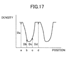
As shown in FIG. 17, if there is some dust or a sensor
has some trouble, the abnormal pixel data represents a
sharp density fluctuation at some positions. For
example, suppose that sampling points a, b, c and d have
densities Da, Db, Dc and Dd, respectively. If the
sampling points have deviations of their densities out
of a predetermined range, the abnormal pixel average
density computing part 72 considers the sampling points
out of the range to be candidates of an abnormal pixel
and computes density gradients of the sampling points.
As shown in FIG. 17, if the density level decreases from
the point a to the point b and increases from the point
c to the point d, the abnormal pixel average density
computing part 72 can identify positions of the abnormal
pixels in a range between the point a and the point d.
Then, the abnormal pixel average density computing part
72 computes an average density of the abnormal pixels,
which is stored in the buffer memory 26.
A description will now be given of
correction of the image data read from the manuscript 13
on the basis of a position and a density of an abnormal
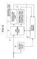
pixel. As shown in a block diagram in FIG. 18, the
abnormal pixel correcting part 28 comprises a density
correcting part 72, an MTF correcting part 73, an MTF
weak-correcting part 74 and a selecting part 75.
Regarding the abnormal pixel information stored in the
buffer memory 26, the density correcting part 72 refers
to density information of an abnormal pixel that has
been detected in the abnormal pixel detecting part 27
with respect to both in the main-scan direction and in
the sub-scan direction. Then, the density correcting
part 72 subtracts an average density computed by the
abnormal pixel detecting part 27 from a density of the
abnormal pixel to correct the density level of the
abnormal pixel. Then, the MTF correcting part 73 and
the MTF weak-correcting part 74 perform sharpness
correction for the resulting image data. The MTF
correcting part 73 corrects the image data in accordance
with a normal level of sharpness, and the MTF correcting
part 74 corrects pixels in the neighborhood of the
abnormal pixel in accordance with a lower level of
sharpness. As a result, a black streak caused by the
abnormal pixel almost disappears. Although the black
streak cannot be removed completely and there remains a
slight trace of the black streak, information included
in the manuscript can be restored. Also, through the
slight trace, it can be determined whether or not the
correction for the black streak has been performed,
thereby urging an operator to observe pixels surrounding
the abnormal pixel carefully.
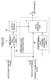
On the other hand, as shown in a block
diagram in FIG. 19, the abnormal pixel correcting part
28 may comprise a surrounding pixel statistic operating
part 76 and a data switching part 77 to correct the
image data of the manuscript 13 through interpolation by
using statistic data. In this case, when the image of
the manuscript 13 is read, the surrounding pixel
statistic operating part 76 computes statistics helpful
to maintain continuity between an abnormal pixel to be
corrected and its surrounding pixels with reference to
abnormal pixel data stored in the buffer memory 26. The
statistics may include a density average and a density
gradient with respect to a plurality of lines to be
corrected. The statistics may include an
autocorrelation of a discrete dot, which is an
informative statistic to maintain the continuity.
According to the statistics derived from the surrounding
pixel statistic operating part 76, the data switching
part 77 generates a substitution pixel to substitute the
abnormal pixel in the read image data for the
substitution pixel.
A description will now be given, with
reference to FIG. 20, of an example in which the
abnormal pixel correcting part 28 uses the statistics to
correct the read image data. The abnormal pixel
correcting part 28 maintains a flag in a position where
an abnormal pixel has been detected. A detected signal
"1" means that the pixel in the position is abnormal,
and a detected signal "0", by contrast, means that the
pixel in the position is normal. The abnormal pixel
correcting part 28 determines reference pixels, which
serve to correct the abnormal pixels, in the
neighborhood of the detected abnormal pixels. The
reference pixels are points a and b. The point a is
located at the position before the detected abnormal
pixel, and the point b is located at the position after
the detected abnormal pixel. These points a and b
should be located at positions where the abnormal pixel
has no influence on the points. The abnormal pixel
correcting part 28 performs sampling of density
information of the read image data from the manuscript
13. Let an input density at the point a be Da and an
input density at the point b be Db. The abnormal pixel
correcting part 28 uses the input densities Da and Db to
compute correction density. Linear interpolation is a
statistical correcting method to compute the correction
density. A density step ΔD is computed as follows; ΔD
= (Db - Da) / (b - a). A density of each abnormal pixel
is substituted for an interpolating density D as
follows; D = Da + n×ΔD, where the notation n represents
a distance between the point a and a position of the
abnormal pixel. In a case that the manuscript 13 is
solid, that is, the densities Da and Db have the almost
same value, the correction density of an abnormal pixel
resulting in a vertical streak is substituted for the
input density Da or Db. On the other hand, in a case
that there is a difference of the density between the
points a and b, if the abnormal pixel should is
corrected to have the same density as the input density
Da, the parameter gives adverse influence to a corrected
density of the abnormal pixel, thereby producing density
mixture with neighboring pixels of the abnormal pixel in
the shape of the vertical streak. Although the
resulting image under the latter case makes a greater
deal of improvement than the vertical streak showing up
without any correction, the resulting image is inferior
to the original image of the manuscript 13. Accordingly,
the operator needs to check whether or not the
correction is useful.
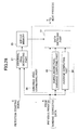
As shown in a block diagram in FIG. 21, the
abnormal pixel correcting part 28 may comprise a
corrected pixel computing part 81 and a data switching
part 77. In this case, the reading part 1 reads a null-image
in order to detect dust on the surface of the
contact glass before the manuscript 13 is actually read.
The detection process starts by receiving an enable
signal of a detection starting signal C. The abnormal
pixel detecting part 27 receives the image data to be
detected, binarizes a line of the image data and stores
the binarized line of the image data in the buffer
memory 26. In this case, it is assumed that an abnormal
pixel is caused by an object on the surface of the
contact glass that obstructs an input of the reflected
light to the CCD 7. At the reading of the white back
board 44b, if black dust is lying on the surface of the
contact glass, a density level of the corresponding
pixel becomes high. On the other hand, at the reading
of the black back board 44a, if white dust is lying on
the surface of the contact glass, a density level of the
corresponding pixel becomes low. At the reading of the
white back board 44b, in the binarized data in the
buffer memory 26, a pixel at a position where "0" is
written is normal and, by contrast, a pixel at a
position where "1" is written is abnormal. On the other
hand, at the reading of the black back board 44a, in the
binarized data in the buffer memory 26, a pixel at a
position where "1" is written is normal and, by contrast,
a pixel at a position where "0" is written is abnormal.
Then, the SDF 10 delivers the manuscript
13 on the surface of the contact glass. The CCD 7 reads
each line of the delivered manuscript 13 as a line data.
After completing the shading correction, the resulting
image data is delivered to the data switching part 77
and the corrected pixel computing part 81 as input image
data A. The corrected pixel computing part 81 generates
a 3×3 pixel matrix 82 whose center of pixels is e as
shown in FIG. 22. Using the pixel matrix 82, the
corrected pixel computing part 81 performs correction if
the pixel e is abnormal. The data switching part 77
performs with reference to data stored in the buffer
memory 26 as follows; If the pixel concerned has the
signal "1" for the white back board 44b or the signal
"0" for the black board 44a, the data switching part 77
delivers the image data produced by the corrected pixel
computing part 81 to the next process as image data B.
On the other hand, if the pixel concerned has the signal
"0" for the white back board 44b or the signal "1" for
the black board 44a, the data switching part 77 delivers
the input image data A to the next process. In this
manner, the image scanning apparatus surely detects and
corrects an abnormal pixel caused by the dust.
As shown in FIG. 23, the abnormal
pixel
correcting part 28 may comprise a surrounding pixel
variance computing part 83 and the
data switching part
77. In this case, the surrounding pixel
variance
computing part 83 computes variances of the image data
with respect to both the main-scan direction and the
sub-scan direction from the surrounding pixels for the
input image data A. When the pixel e should be
corrected, the 3×3
pixel matrix 82 is used as shown in
FIG. 22 for the correction under the surrounding pixel
variance computing part 83. The 3×3
pixel matrix 82
has pixels a, b, c, d, f, g, h and i surrounding the
pixel e to be corrected. Let each density of the
surrounding pixels be Da, Db, Dc, Dd, Df, Dg, Dh and Di,
respectively. For example, suppose that the pixels b, e
and h are abnormal. Then, these pixels are set aside at
the correction. The correction data is selected among
variances of three directions: a horizontal direction, a
right-rising diagonal and a right-falling diagonal,
where the variances in the horizontal direction, in the
right-rising direction and in the right-falling
direction are computed by the following formulae,
respectively:
Among the three variances, a direction with a minimal
variance is selected and the pixel e to be corrected is
interpolated by using an average in the selected
direction. For example, if the variance in the
horizontal direction is minimal, the pixel e to be
corrected is interpolated by an average (Dd+Df)/2.
As shown in a block diagram in FIG. 24, the
abnormal pixel correcting part 28 may comprise an
average computing part 84 and the data switching part 77.
The average computing part 84 computes the density level
De of the pixel e to be corrected from the density
levels of the surrounding pixels as follows;
De = (Da + Dc + Dd + Df + Dg + Di)/6, where the pixels b,
e and h are set aside because it is assumed that these
three pixels are abnormal.
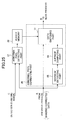
As shown in a block diagram in FIG. 25, the
abnormal pixel correcting part 28 may comprise a maximum
detecting part 85, the average computing part 84 and the
data switching part 77. In this case, the maximum
detecting part 85 sorts the left-side pixels a, d and g
in the 3×3 pixel matrix 82 in descending order
regarding the density level. Suppose that Da > Dd > Dg.
Then, the maximum detecting part 85 sorts the right-side
pixels c, f and i in the 3×3 pixel matrix 82 in the
same order. Suppose that Di > Df > Dc. The maximum
detecting part 85 delivers the left-side maximal density
level Da and the right-side maximal density level Di to
the average computing part 84. The average computing
part 84 computes an average De = (Da+Di)/2 and delivers
the result to the data switching part 77. If the pixel
e is abnormal, the data switching part 77 delivers the
average density De to the next process. If the pixel e
is normal, the data switching part 77 delivers the input
data A to the next process as an input data B.
As shown in a block diagram in FIG. 26, the
abnormal pixel correcting part 28 may comprise a
binarization/measurement processing part 86, a dynamic
average computing part 87 and the data switching part 77.
In this case, the binarization/measurement processing
part 86 binarizes surrounding pixels of the 3×3 pixel
matrix 82, counts the number of "0"s, which is notated
as an NW and the number of "1"s, which is notated as an
NB and delivers position information of pixels belonging
to a collection of pixels with bigger number to the
dynamic average computing part 87. The dynamic average
computing part 87 computes an average density by using
the position information delivered by the
binarization/measurement processing part 86 and the
input image data A in the matrix. For example, it is
assumed that a result of the binarization is shown in a
matrix 88 in FIG. 27. Since the pixels b, e and h are
assumed as abnormal pixels, the NB is equal to 4 and the
NW is equal to 2. Using the pixels a, c, d and i whose
collection has the bigger number 4, the dynamic average
computing part 87 computes the density De as follws;
De = (Da + Dc + Dd + Di)/4, and delivers the density De
to the data switching part 77. If the pixel e is
abnormal, the data switching part 77 delivers the
density De to the next process. If the pixel e is
normal, the data switching part 77 delivers the input
data A to the next process as an input data B.
As shown in a block diagram in FIG. 28, the
abnormal pixel correcting part 28 may comprise the
surrounding pixel variance computing part 83, the
average computing part 84 and the data switching part 77.
It is assumed that the image scanning apparatus has two
modes, a character mode and a picture mode. The
character mode is suitable for processing the manuscript
13 whose contents are mainly formed of characters. The
picture mode is suitable for processing a printed
picture formed of dots. Suppose that a mode signal D
has "0" in the character mode and "1" in the picture
mode. When the mode signal D has "0", the surrounding
pixel variance computing part 83 performs correction by
computing an average of surrounding pixels in the
direction with a minimal variance. When the mode signal
D has "1", the average computing part 84 performs
correction by computing an average of surrounding pixels.
According to the position information of an abnormal
pixel and the mode signal D, if the pixel e is abnormal,
the data switching part 77 delivers the resulting
density De to the next process, and if the pixel e is
normal, the data switching part 77 delivers the input
data A to the next process as an input data B.
A result of the correction is illustrated in
pattern diagrams in FIG. 29A through FIG. 29C. FIG. 29A
illustrates data containing abnormal pixel 57 stored in
the buffer memory 26. In this diagram, a black streak
90 is information indicating a position of a abnormal
pixel. FIG. 29B illustrates an image 91 read from the
manuscript 13. In this diagram, there are many black
streaks 92 caused by abnormal pixels, thereby having
trouble transferring information of the manuscript 13.
FIG. 29C illustrates an image 93 resulting from
correcting the image 91. In the resulting image 93, a
considerable number of black streaks are deleted. The
image data 93 is interpolated by using surrounding
pixels in the main-scan direction. As a result, if a
corrected range originates from a white-solid range or a
black-solid range, corrected density does not
deteriorate because the correction uses uniform density
of the solid range. However, a density difference may
be identified from the neighborhood of the abnormal
pixel, because the correction uses a variance of the
density level. The abnormal pixel data 57 and the image
93 are displayed under the operation displaying part 23
so that an operator can set a level of correction freely.
As a result, the operator can obtain an image that the
operator recognizes to be appropriate. In this case,
when the correction is performed to the extent that the
black streaks are completely deleted, a dot range of the
manuscript 13 deteriorates in comparison with the
original one. Even if the correction is not performed
to the extent, the number of the black streaks 92
decreases as shown in FIG. 29C. Accordingly, there is
great improvement on image recognition.
A description will now be given, with
reference to flowcharts of FIG. 30 and FIG. 31, of
procedures for a preview process of the abnormal pixel
data 57 and the corrected image 93. Suppose that there
are a plurality of the manuscripts 13. In this setting,
two possibilities regarding the preview process are
considered. One is the case that a result of preview
process is determined on the basis of just a first sheet
of the manuscripts 13. In this case, after the first
sheet of the manuscripts 13 is read and the correcting
process is performed for the read image (step S11), the
abnormal pixel data 57 in the buffer memory 26 and the
corrected image 93 in the image data memory part 21 are
positioned so that positions of the common abnormal
pixels contained in the two data can be just fitted.
Then, the result is displayed on the operation
displaying part 23. For the displayed result, the
preview process prompts an operator to set hereafter
processes (step S12). Through the display, the operator
can check the extent of the density mixture in a dot
range and the lack of character information caused by
vertical streaks. If the operator determines to
maintain current setting in order to incorporate the
correction result for hereafter processes (step S13),
the operator instructs the abnormal pixel correcting
part 28 to perform the same correction for all sheets of
the manuscripts 13 (step S14). When all sheets of the
manuscripts 13 are corrected, the detecting process of
the abnormal pixels is performed for each sheet of the
manuscripts 13. Accordingly, a detection result of the
abnormal pixels may differ from each other depending on
reading conditions.
If the operator determines to alter the
current setting in order not to incorporate the
correction result, the operator instructs the abnormal
pixel correcting part 28 to alter a condition of the
correcting process and performs correction (step S15).
In this case, if the operator is not so concerned about
the vertical streaks and there is outstanding influence
caused by the image correction because the manuscripts
13 are mainly formed of halftones, the operator
instructs the abnormal pixel correcting part 28 not to
perform correction without interpolating any pixel. The
operator then instructs the abnormal pixel correcting
part 28 not to correct any sheet of the manuscripts 13
(step S16). If the operator is concerned about vertical
streaks and there is outstanding influence caused by the
image correction, the operator alters a parameter for
the abnormal pixel detection or a parameter involved in
a corrected range on the operation displaying part 23 in
order to perform correction and read image again. If
the operator realizes the limited improvement of the
image quality just through the alternation of the
parameters, the operator cleans up the reading surface
of the SDF 10 to remove factors causing trouble and read
again (step S17) .
The other is the case that all sheets of the
manuscripts 13 are processed and the operator determines
the whole processes from one of the sheets. As shown in
FIG. 31, after the image scanning apparatus reads all of
the sheets and performs the correcting process for the
abnormal pixels (step S21), the preview process displays
an arbitrary sheet of the abnormal pixel data 57 stored
in the buffer memory and the corrected image 93 stored
in the image data memory part 21 on the operation
displaying part 23 (step S22). When one sheet of the
corrected image 93 is displayed, the operator operates
the operation displaying part 23 to select a preview
image of an arbitrary sheet of the manuscripts 13.
Through the display, the operator determines whether or
not the correcting process should be valid (step S23).
If the operator realizes that the correction is
performed successfully, the operator maintains the
current status and transfer the corrected image 93 to an
external device (step S24). If the operator realizes
that the correction is unsuccessful, the operator alters
the current status (step S25) and the manuscripts are
read one more time (step S21).
In this manner, a high quality image without
any black and white streak caused by an abnormal pixel
is obtained.
The description has been given of the case
that when the abnormal pixel detecting part 27 detects
an abnormal pixel caused by dust on the surface of the
contact glass, the abnormal pixel correcting part 28
corrects the abnormal pixel. However, if there remains
the dust on the surface of the contact glass, an
abnormal pixel would be detected again. In order to
prevent this situation, as shown in a block diagram in
FIG. 32, when the abnormal pixel detecting part 27
detects an abnormal pixel caused by dust on the surface
of the contact glass, the abnormal pixel detecting part
27 sends an abnormal pixel detection signal to an alarm
display control part 94. When the alarm display control
part 94 receives the abnormal pixel detection signal,
the alarm display control part 94 lets the operation
displaying part 23 display information indicating that
the contact glass should be cleaned up. The alarm
display control part 94 identifies a position on the
contact glass where dust is lying from a position of the
abnormal pixel contained in the abnormal pixel detection
signal. As shown in FIG. 33, the operation displaying
part 23 designates the position by an arrowhead and
displays a message "Clean the surface of the contact
glass." to urge the operator to clean up the contact
glass.
Also, when an abnormal pixel is detected, the
image scanning apparatus may clean the contact glass
automatically. In this case, as shown in a block
diagram in FIG. 34, when the abnormal pixel detecting
part 27 detects an abnormal pixel caused by dust on the
surface of the contact glass, the abnormal pixel
detecting part 27 sends the abnormal pixel detection
signal to a cleaning control part 95. When receiving
the abnormal pixel detection signal, the cleaning
control part 95 lets a cleaning part 96 clean up the
surface of the contact glass. As shown in FIG. 35A, the
cleaning part 96 may have a rolling cleaning part 96a at
a position tangential to a contact glass 97 of the SDF
10. Also, as shown in FIG. 35B, an air blowout part 96b
is installed in the SDF 10 so that the air can blow out
dust on the contact glass 97. In this manner, the
automatic removal of the dust prevents an abnormal pixel
to obtain a high quality image reliably.
The present invention is not limited to the
specifically disclosed embodiments, and variations and
modifications may be made without departing from the
scope of the present invention.
The present application is based on Japanese
priority application No. 2001-328888 filed October 26,
2001, the entire contents of which are hereby
incorporated by reference.