EP1306908A1 - Piezoelectric/electrostrictive device and method of producing the same - Google Patents
Piezoelectric/electrostrictive device and method of producing the same Download PDFInfo
- Publication number
- EP1306908A1 EP1306908A1 EP01938552A EP01938552A EP1306908A1 EP 1306908 A1 EP1306908 A1 EP 1306908A1 EP 01938552 A EP01938552 A EP 01938552A EP 01938552 A EP01938552 A EP 01938552A EP 1306908 A1 EP1306908 A1 EP 1306908A1
- Authority
- EP
- European Patent Office
- Prior art keywords
- piezoelectric
- movable parts
- base
- electrostrictive
- parts
- Prior art date
- Legal status (The legal status is an assumption and is not a legal conclusion. Google has not performed a legal analysis and makes no representation as to the accuracy of the status listed.)
- Withdrawn
Links
- 238000000034 method Methods 0.000 title claims description 60
- 239000000853 adhesive Substances 0.000 claims abstract description 75
- 230000001070 adhesive effect Effects 0.000 claims abstract description 75
- 239000000919 ceramic Substances 0.000 claims description 107
- 239000000463 material Substances 0.000 claims description 54
- 229910052751 metal Inorganic materials 0.000 claims description 40
- 239000002184 metal Substances 0.000 claims description 40
- 238000006073 displacement reaction Methods 0.000 claims description 36
- 238000005520 cutting process Methods 0.000 claims description 30
- 238000001354 calcination Methods 0.000 claims description 23
- 238000010030 laminating Methods 0.000 claims description 17
- 238000003475 lamination Methods 0.000 claims description 16
- 238000005452 bending Methods 0.000 claims description 12
- 238000011161 development Methods 0.000 claims description 4
- 238000005304 joining Methods 0.000 description 37
- 239000010408 film Substances 0.000 description 19
- 238000004519 manufacturing process Methods 0.000 description 18
- MCMNRKCIXSYSNV-UHFFFAOYSA-N Zirconium dioxide Chemical compound O=[Zr]=O MCMNRKCIXSYSNV-UHFFFAOYSA-N 0.000 description 14
- 230000008569 process Effects 0.000 description 14
- 230000006870 function Effects 0.000 description 11
- 229920005989 resin Polymers 0.000 description 11
- 239000011347 resin Substances 0.000 description 11
- BASFCYQUMIYNBI-UHFFFAOYSA-N platinum Chemical compound [Pt] BASFCYQUMIYNBI-UHFFFAOYSA-N 0.000 description 9
- 239000000203 mixture Substances 0.000 description 8
- 239000007769 metal material Substances 0.000 description 7
- 239000000843 powder Substances 0.000 description 7
- CPLXHLVBOLITMK-UHFFFAOYSA-N Magnesium oxide Chemical compound [Mg]=O CPLXHLVBOLITMK-UHFFFAOYSA-N 0.000 description 6
- VYPSYNLAJGMNEJ-UHFFFAOYSA-N Silicium dioxide Chemical compound O=[Si]=O VYPSYNLAJGMNEJ-UHFFFAOYSA-N 0.000 description 6
- 238000004140 cleaning Methods 0.000 description 6
- 150000001875 compounds Chemical class 0.000 description 6
- 239000000470 constituent Substances 0.000 description 6
- 230000000694 effects Effects 0.000 description 6
- 230000008859 change Effects 0.000 description 5
- 239000002002 slurry Substances 0.000 description 5
- 239000000758 substrate Substances 0.000 description 5
- XEEYBQQBJWHFJM-UHFFFAOYSA-N Iron Chemical compound [Fe] XEEYBQQBJWHFJM-UHFFFAOYSA-N 0.000 description 4
- PXHVJJICTQNCMI-UHFFFAOYSA-N Nickel Chemical compound [Ni] PXHVJJICTQNCMI-UHFFFAOYSA-N 0.000 description 4
- KDLHZDBZIXYQEI-UHFFFAOYSA-N Palladium Chemical compound [Pd] KDLHZDBZIXYQEI-UHFFFAOYSA-N 0.000 description 4
- 239000010931 gold Substances 0.000 description 4
- 239000000395 magnesium oxide Substances 0.000 description 4
- 229910002077 partially stabilized zirconia Inorganic materials 0.000 description 4
- 229910052697 platinum Inorganic materials 0.000 description 4
- 229910002076 stabilized zirconia Inorganic materials 0.000 description 4
- BQCADISMDOOEFD-UHFFFAOYSA-N Silver Chemical compound [Ag] BQCADISMDOOEFD-UHFFFAOYSA-N 0.000 description 3
- FKSZLDCMQZJMFN-UHFFFAOYSA-N [Mg].[Pb] Chemical compound [Mg].[Pb] FKSZLDCMQZJMFN-UHFFFAOYSA-N 0.000 description 3
- PNEYBMLMFCGWSK-UHFFFAOYSA-N aluminium oxide Inorganic materials [O-2].[O-2].[O-2].[Al+3].[Al+3] PNEYBMLMFCGWSK-UHFFFAOYSA-N 0.000 description 3
- 238000005219 brazing Methods 0.000 description 3
- 229910010293 ceramic material Inorganic materials 0.000 description 3
- 238000005229 chemical vapour deposition Methods 0.000 description 3
- 230000003247 decreasing effect Effects 0.000 description 3
- NKZSPGSOXYXWQA-UHFFFAOYSA-N dioxido(oxo)titanium;lead(2+) Chemical compound [Pb+2].[O-][Ti]([O-])=O NKZSPGSOXYXWQA-UHFFFAOYSA-N 0.000 description 3
- 239000003822 epoxy resin Substances 0.000 description 3
- 239000011521 glass Substances 0.000 description 3
- PCHJSUWPFVWCPO-UHFFFAOYSA-N gold Chemical compound [Au] PCHJSUWPFVWCPO-UHFFFAOYSA-N 0.000 description 3
- 229910052737 gold Inorganic materials 0.000 description 3
- SIWVEOZUMHYXCS-UHFFFAOYSA-N oxo(oxoyttriooxy)yttrium Chemical compound O=[Y]O[Y]=O SIWVEOZUMHYXCS-UHFFFAOYSA-N 0.000 description 3
- 229920000647 polyepoxide Polymers 0.000 description 3
- -1 polyethylene terephthalate Polymers 0.000 description 3
- 238000007639 printing Methods 0.000 description 3
- 238000007650 screen-printing Methods 0.000 description 3
- 239000000377 silicon dioxide Substances 0.000 description 3
- 229910052709 silver Inorganic materials 0.000 description 3
- 239000004332 silver Substances 0.000 description 3
- 239000000725 suspension Substances 0.000 description 3
- VYZAMTAEIAYCRO-UHFFFAOYSA-N Chromium Chemical compound [Cr] VYZAMTAEIAYCRO-UHFFFAOYSA-N 0.000 description 2
- ZOKXTWBITQBERF-UHFFFAOYSA-N Molybdenum Chemical compound [Mo] ZOKXTWBITQBERF-UHFFFAOYSA-N 0.000 description 2
- ATJFFYVFTNAWJD-UHFFFAOYSA-N Tin Chemical compound [Sn] ATJFFYVFTNAWJD-UHFFFAOYSA-N 0.000 description 2
- HCHKCACWOHOZIP-UHFFFAOYSA-N Zinc Chemical compound [Zn] HCHKCACWOHOZIP-UHFFFAOYSA-N 0.000 description 2
- LIABKAQKQSUQJX-UHFFFAOYSA-N [Mn].[Pb] Chemical compound [Mn].[Pb] LIABKAQKQSUQJX-UHFFFAOYSA-N 0.000 description 2
- 239000000654 additive Substances 0.000 description 2
- 239000000956 alloy Substances 0.000 description 2
- 229910045601 alloy Inorganic materials 0.000 description 2
- 230000008901 benefit Effects 0.000 description 2
- 239000011230 binding agent Substances 0.000 description 2
- FSAJRXGMUISOIW-UHFFFAOYSA-N bismuth sodium Chemical compound [Na].[Bi] FSAJRXGMUISOIW-UHFFFAOYSA-N 0.000 description 2
- BRPQOXSCLDDYGP-UHFFFAOYSA-N calcium oxide Chemical compound [O-2].[Ca+2] BRPQOXSCLDDYGP-UHFFFAOYSA-N 0.000 description 2
- 239000000292 calcium oxide Substances 0.000 description 2
- ODINCKMPIJJUCX-UHFFFAOYSA-N calcium oxide Inorganic materials [Ca]=O ODINCKMPIJJUCX-UHFFFAOYSA-N 0.000 description 2
- 229910000420 cerium oxide Inorganic materials 0.000 description 2
- 229910052804 chromium Inorganic materials 0.000 description 2
- 239000011651 chromium Substances 0.000 description 2
- 229910017052 cobalt Inorganic materials 0.000 description 2
- 239000010941 cobalt Substances 0.000 description 2
- GUTLYIVDDKVIGB-UHFFFAOYSA-N cobalt atom Chemical compound [Co] GUTLYIVDDKVIGB-UHFFFAOYSA-N 0.000 description 2
- 239000013078 crystal Substances 0.000 description 2
- 230000007423 decrease Effects 0.000 description 2
- 230000005684 electric field Effects 0.000 description 2
- 239000007772 electrode material Substances 0.000 description 2
- 238000001962 electrophoresis Methods 0.000 description 2
- 238000005530 etching Methods 0.000 description 2
- 238000010438 heat treatment Methods 0.000 description 2
- 230000010354 integration Effects 0.000 description 2
- 229910052742 iron Inorganic materials 0.000 description 2
- 229910052746 lanthanum Inorganic materials 0.000 description 2
- FZLIPJUXYLNCLC-UHFFFAOYSA-N lanthanum atom Chemical compound [La] FZLIPJUXYLNCLC-UHFFFAOYSA-N 0.000 description 2
- 229910052451 lead zirconate titanate Inorganic materials 0.000 description 2
- AXZKOIWUVFPNLO-UHFFFAOYSA-N magnesium;oxygen(2-) Chemical compound [O-2].[Mg+2] AXZKOIWUVFPNLO-UHFFFAOYSA-N 0.000 description 2
- 150000002739 metals Chemical class 0.000 description 2
- 229910052750 molybdenum Inorganic materials 0.000 description 2
- 239000011733 molybdenum Substances 0.000 description 2
- 238000000465 moulding Methods 0.000 description 2
- 229910052759 nickel Inorganic materials 0.000 description 2
- 229910052758 niobium Inorganic materials 0.000 description 2
- 239000010955 niobium Substances 0.000 description 2
- GUCVJGMIXFAOAE-UHFFFAOYSA-N niobium atom Chemical compound [Nb] GUCVJGMIXFAOAE-UHFFFAOYSA-N 0.000 description 2
- BMMGVYCKOGBVEV-UHFFFAOYSA-N oxo(oxoceriooxy)cerium Chemical compound [Ce]=O.O=[Ce]=O BMMGVYCKOGBVEV-UHFFFAOYSA-N 0.000 description 2
- UZLYXNNZYFBAQO-UHFFFAOYSA-N oxygen(2-);ytterbium(3+) Chemical compound [O-2].[O-2].[O-2].[Yb+3].[Yb+3] UZLYXNNZYFBAQO-UHFFFAOYSA-N 0.000 description 2
- 229910052763 palladium Inorganic materials 0.000 description 2
- 239000002245 particle Substances 0.000 description 2
- 238000007747 plating Methods 0.000 description 2
- 239000002243 precursor Substances 0.000 description 2
- 238000002360 preparation method Methods 0.000 description 2
- 238000012545 processing Methods 0.000 description 2
- 230000009467 reduction Effects 0.000 description 2
- 229910000679 solder Inorganic materials 0.000 description 2
- 238000004544 sputter deposition Methods 0.000 description 2
- 229910052712 strontium Inorganic materials 0.000 description 2
- CIOAGBVUUVVLOB-UHFFFAOYSA-N strontium atom Chemical compound [Sr] CIOAGBVUUVVLOB-UHFFFAOYSA-N 0.000 description 2
- 229910052715 tantalum Inorganic materials 0.000 description 2
- GUVRBAGPIYLISA-UHFFFAOYSA-N tantalum atom Chemical compound [Ta] GUVRBAGPIYLISA-UHFFFAOYSA-N 0.000 description 2
- 239000010409 thin film Substances 0.000 description 2
- 229910052718 tin Inorganic materials 0.000 description 2
- 229910000314 transition metal oxide Inorganic materials 0.000 description 2
- WFKWXMTUELFFGS-UHFFFAOYSA-N tungsten Chemical compound [W] WFKWXMTUELFFGS-UHFFFAOYSA-N 0.000 description 2
- 229910052721 tungsten Inorganic materials 0.000 description 2
- 239000010937 tungsten Substances 0.000 description 2
- 238000004017 vitrification Methods 0.000 description 2
- 229910003454 ytterbium oxide Inorganic materials 0.000 description 2
- 229940075624 ytterbium oxide Drugs 0.000 description 2
- 229910052725 zinc Inorganic materials 0.000 description 2
- 239000011701 zinc Substances 0.000 description 2
- OYPRJOBELJOOCE-UHFFFAOYSA-N Calcium Chemical compound [Ca] OYPRJOBELJOOCE-UHFFFAOYSA-N 0.000 description 1
- RYGMFSIKBFXOCR-UHFFFAOYSA-N Copper Chemical compound [Cu] RYGMFSIKBFXOCR-UHFFFAOYSA-N 0.000 description 1
- 239000004831 Hot glue Substances 0.000 description 1
- WHXSMMKQMYFTQS-UHFFFAOYSA-N Lithium Chemical compound [Li] WHXSMMKQMYFTQS-UHFFFAOYSA-N 0.000 description 1
- KJTLSVCANCCWHF-UHFFFAOYSA-N Ruthenium Chemical compound [Ru] KJTLSVCANCCWHF-UHFFFAOYSA-N 0.000 description 1
- 229910052581 Si3N4 Inorganic materials 0.000 description 1
- GWEVSGVZZGPLCZ-UHFFFAOYSA-N Titan oxide Chemical compound O=[Ti]=O GWEVSGVZZGPLCZ-UHFFFAOYSA-N 0.000 description 1
- RTAQQCXQSZGOHL-UHFFFAOYSA-N Titanium Chemical compound [Ti] RTAQQCXQSZGOHL-UHFFFAOYSA-N 0.000 description 1
- PYPDMIQMPWEFHX-UHFFFAOYSA-N [Pb].[Co] Chemical compound [Pb].[Co] PYPDMIQMPWEFHX-UHFFFAOYSA-N 0.000 description 1
- VNSWULZVUKFJHK-UHFFFAOYSA-N [Sr].[Bi] Chemical compound [Sr].[Bi] VNSWULZVUKFJHK-UHFFFAOYSA-N 0.000 description 1
- 230000001133 acceleration Effects 0.000 description 1
- 230000009471 action Effects 0.000 description 1
- 230000000996 additive effect Effects 0.000 description 1
- 238000005054 agglomeration Methods 0.000 description 1
- 230000002776 aggregation Effects 0.000 description 1
- 229910052782 aluminium Inorganic materials 0.000 description 1
- XAGFODPZIPBFFR-UHFFFAOYSA-N aluminium Chemical compound [Al] XAGFODPZIPBFFR-UHFFFAOYSA-N 0.000 description 1
- 229910052787 antimony Inorganic materials 0.000 description 1
- WATWJIUSRGPENY-UHFFFAOYSA-N antimony atom Chemical compound [Sb] WATWJIUSRGPENY-UHFFFAOYSA-N 0.000 description 1
- QQHJESKHUUVSIC-UHFFFAOYSA-N antimony lead Chemical compound [Sb].[Pb] QQHJESKHUUVSIC-UHFFFAOYSA-N 0.000 description 1
- 229910052788 barium Inorganic materials 0.000 description 1
- DSAJWYNOEDNPEQ-UHFFFAOYSA-N barium atom Chemical compound [Ba] DSAJWYNOEDNPEQ-UHFFFAOYSA-N 0.000 description 1
- JRPBQTZRNDNNOP-UHFFFAOYSA-N barium titanate Chemical compound [Ba+2].[Ba+2].[O-][Ti]([O-])([O-])[O-] JRPBQTZRNDNNOP-UHFFFAOYSA-N 0.000 description 1
- 229910002113 barium titanate Inorganic materials 0.000 description 1
- 230000015572 biosynthetic process Effects 0.000 description 1
- 229910052797 bismuth Inorganic materials 0.000 description 1
- JCXGWMGPZLAOME-UHFFFAOYSA-N bismuth atom Chemical compound [Bi] JCXGWMGPZLAOME-UHFFFAOYSA-N 0.000 description 1
- 238000005422 blasting Methods 0.000 description 1
- 229910052793 cadmium Inorganic materials 0.000 description 1
- BDOSMKKIYDKNTQ-UHFFFAOYSA-N cadmium atom Chemical compound [Cd] BDOSMKKIYDKNTQ-UHFFFAOYSA-N 0.000 description 1
- 229910052792 caesium Inorganic materials 0.000 description 1
- TVFDJXOCXUVLDH-UHFFFAOYSA-N caesium atom Chemical compound [Cs] TVFDJXOCXUVLDH-UHFFFAOYSA-N 0.000 description 1
- 229910052791 calcium Inorganic materials 0.000 description 1
- 239000011575 calcium Substances 0.000 description 1
- 238000003490 calendering Methods 0.000 description 1
- 239000003575 carbonaceous material Substances 0.000 description 1
- 238000005266 casting Methods 0.000 description 1
- 239000004568 cement Substances 0.000 description 1
- 238000005253 cladding Methods 0.000 description 1
- 238000000576 coating method Methods 0.000 description 1
- 238000004891 communication Methods 0.000 description 1
- 238000010276 construction Methods 0.000 description 1
- 229910052802 copper Inorganic materials 0.000 description 1
- 239000010949 copper Substances 0.000 description 1
- PMHQVHHXPFUNSP-UHFFFAOYSA-M copper(1+);methylsulfanylmethane;bromide Chemical compound Br[Cu].CSC PMHQVHHXPFUNSP-UHFFFAOYSA-M 0.000 description 1
- 230000000593 degrading effect Effects 0.000 description 1
- 238000010586 diagram Methods 0.000 description 1
- 238000007598 dipping method Methods 0.000 description 1
- 239000002270 dispersing agent Substances 0.000 description 1
- 238000007606 doctor blade method Methods 0.000 description 1
- 239000000428 dust Substances 0.000 description 1
- 238000010894 electron beam technology Methods 0.000 description 1
- 239000000839 emulsion Substances 0.000 description 1
- 238000001704 evaporation Methods 0.000 description 1
- 230000008020 evaporation Effects 0.000 description 1
- 238000004299 exfoliation Methods 0.000 description 1
- 238000007733 ion plating Methods 0.000 description 1
- 238000010884 ion-beam technique Methods 0.000 description 1
- 229910052741 iridium Inorganic materials 0.000 description 1
- GKOZUEZYRPOHIO-UHFFFAOYSA-N iridium atom Chemical compound [Ir] GKOZUEZYRPOHIO-UHFFFAOYSA-N 0.000 description 1
- 239000011133 lead Substances 0.000 description 1
- JQJCSZOEVBFDKO-UHFFFAOYSA-N lead zinc Chemical compound [Zn].[Pb] JQJCSZOEVBFDKO-UHFFFAOYSA-N 0.000 description 1
- HFGPZNIAWCZYJU-UHFFFAOYSA-N lead zirconate titanate Chemical compound [O-2].[O-2].[O-2].[O-2].[O-2].[Ti+4].[Zr+4].[Pb+2] HFGPZNIAWCZYJU-UHFFFAOYSA-N 0.000 description 1
- 229910052744 lithium Inorganic materials 0.000 description 1
- 239000000314 lubricant Substances 0.000 description 1
- 238000003754 machining Methods 0.000 description 1
- WPBNNNQJVZRUHP-UHFFFAOYSA-L manganese(2+);methyl n-[[2-(methoxycarbonylcarbamothioylamino)phenyl]carbamothioyl]carbamate;n-[2-(sulfidocarbothioylamino)ethyl]carbamodithioate Chemical compound [Mn+2].[S-]C(=S)NCCNC([S-])=S.COC(=O)NC(=S)NC1=CC=CC=C1NC(=S)NC(=O)OC WPBNNNQJVZRUHP-UHFFFAOYSA-L 0.000 description 1
- 238000010297 mechanical methods and process Methods 0.000 description 1
- 230000005226 mechanical processes and functions Effects 0.000 description 1
- 230000007246 mechanism Effects 0.000 description 1
- 230000004048 modification Effects 0.000 description 1
- 238000012986 modification Methods 0.000 description 1
- 230000003287 optical effect Effects 0.000 description 1
- 239000013307 optical fiber Substances 0.000 description 1
- 239000002985 plastic film Substances 0.000 description 1
- 229920006255 plastic film Polymers 0.000 description 1
- 239000004014 plasticizer Substances 0.000 description 1
- 229920000139 polyethylene terephthalate Polymers 0.000 description 1
- 239000005020 polyethylene terephthalate Substances 0.000 description 1
- 239000011148 porous material Substances 0.000 description 1
- BITYAPCSNKJESK-UHFFFAOYSA-N potassiosodium Chemical compound [Na].[K] BITYAPCSNKJESK-UHFFFAOYSA-N 0.000 description 1
- 238000003672 processing method Methods 0.000 description 1
- 230000009257 reactivity Effects 0.000 description 1
- 230000004043 responsiveness Effects 0.000 description 1
- 229910052703 rhodium Inorganic materials 0.000 description 1
- 239000010948 rhodium Substances 0.000 description 1
- MHOVAHRLVXNVSD-UHFFFAOYSA-N rhodium atom Chemical compound [Rh] MHOVAHRLVXNVSD-UHFFFAOYSA-N 0.000 description 1
- 238000007788 roughening Methods 0.000 description 1
- 229910052707 ruthenium Inorganic materials 0.000 description 1
- 238000005488 sandblasting Methods 0.000 description 1
- 238000000926 separation method Methods 0.000 description 1
- HQVNEWCFYHHQES-UHFFFAOYSA-N silicon nitride Chemical compound N12[Si]34N5[Si]62N3[Si]51N64 HQVNEWCFYHHQES-UHFFFAOYSA-N 0.000 description 1
- 238000005245 sintering Methods 0.000 description 1
- 238000005476 soldering Methods 0.000 description 1
- 238000003980 solgel method Methods 0.000 description 1
- 239000007787 solid Substances 0.000 description 1
- 239000002904 solvent Substances 0.000 description 1
- 230000006641 stabilisation Effects 0.000 description 1
- 238000011105 stabilization Methods 0.000 description 1
- 230000000087 stabilizing effect Effects 0.000 description 1
- 229940071182 stannate Drugs 0.000 description 1
- 239000000126 substance Substances 0.000 description 1
- 230000003746 surface roughness Effects 0.000 description 1
- 238000007669 thermal treatment Methods 0.000 description 1
- 239000011135 tin Substances 0.000 description 1
- 229910052719 titanium Inorganic materials 0.000 description 1
- 239000010936 titanium Substances 0.000 description 1
- OGIDPMRJRNCKJF-UHFFFAOYSA-N titanium oxide Inorganic materials [Ti]=O OGIDPMRJRNCKJF-UHFFFAOYSA-N 0.000 description 1
- 238000007740 vapor deposition Methods 0.000 description 1
- 238000003466 welding Methods 0.000 description 1
- 229910052727 yttrium Inorganic materials 0.000 description 1
- VWQVUPCCIRVNHF-UHFFFAOYSA-N yttrium atom Chemical compound [Y] VWQVUPCCIRVNHF-UHFFFAOYSA-N 0.000 description 1
Images








Classifications
-
- G—PHYSICS
- G11—INFORMATION STORAGE
- G11B—INFORMATION STORAGE BASED ON RELATIVE MOVEMENT BETWEEN RECORD CARRIER AND TRANSDUCER
- G11B5/00—Recording by magnetisation or demagnetisation of a record carrier; Reproducing by magnetic means; Record carriers therefor
- G11B5/48—Disposition or mounting of heads or head supports relative to record carriers ; arrangements of heads, e.g. for scanning the record carrier to increase the relative speed
- G11B5/4806—Disposition or mounting of heads or head supports relative to record carriers ; arrangements of heads, e.g. for scanning the record carrier to increase the relative speed specially adapted for disk drive assemblies, e.g. assembly prior to operation, hard or flexible disk drives
- G11B5/4873—Disposition or mounting of heads or head supports relative to record carriers ; arrangements of heads, e.g. for scanning the record carrier to increase the relative speed specially adapted for disk drive assemblies, e.g. assembly prior to operation, hard or flexible disk drives the arm comprising piezoelectric or other actuators for adjustment of the arm
-
- H—ELECTRICITY
- H10—SEMICONDUCTOR DEVICES; ELECTRIC SOLID-STATE DEVICES NOT OTHERWISE PROVIDED FOR
- H10N—ELECTRIC SOLID-STATE DEVICES NOT OTHERWISE PROVIDED FOR
- H10N30/00—Piezoelectric or electrostrictive devices
- H10N30/01—Manufacture or treatment
- H10N30/09—Forming piezoelectric or electrostrictive materials
- H10N30/093—Forming inorganic materials
- H10N30/097—Forming inorganic materials by sintering
-
- G—PHYSICS
- G11—INFORMATION STORAGE
- G11B—INFORMATION STORAGE BASED ON RELATIVE MOVEMENT BETWEEN RECORD CARRIER AND TRANSDUCER
- G11B5/00—Recording by magnetisation or demagnetisation of a record carrier; Reproducing by magnetic means; Record carriers therefor
- G11B5/48—Disposition or mounting of heads or head supports relative to record carriers ; arrangements of heads, e.g. for scanning the record carrier to increase the relative speed
- G11B5/4806—Disposition or mounting of heads or head supports relative to record carriers ; arrangements of heads, e.g. for scanning the record carrier to increase the relative speed specially adapted for disk drive assemblies, e.g. assembly prior to operation, hard or flexible disk drives
- G11B5/4826—Mounting, aligning or attachment of the transducer head relative to the arm assembly, e.g. slider holding members, gimbals, adhesive
- G11B5/483—Piezoelectric devices between head and arm, e.g. for fine adjustment
-
- H—ELECTRICITY
- H10—SEMICONDUCTOR DEVICES; ELECTRIC SOLID-STATE DEVICES NOT OTHERWISE PROVIDED FOR
- H10N—ELECTRIC SOLID-STATE DEVICES NOT OTHERWISE PROVIDED FOR
- H10N30/00—Piezoelectric or electrostrictive devices
- H10N30/01—Manufacture or treatment
- H10N30/05—Manufacture of multilayered piezoelectric or electrostrictive devices, or parts thereof, e.g. by stacking piezoelectric bodies and electrodes
- H10N30/053—Manufacture of multilayered piezoelectric or electrostrictive devices, or parts thereof, e.g. by stacking piezoelectric bodies and electrodes by integrally sintering piezoelectric or electrostrictive bodies and electrodes
-
- H—ELECTRICITY
- H10—SEMICONDUCTOR DEVICES; ELECTRIC SOLID-STATE DEVICES NOT OTHERWISE PROVIDED FOR
- H10N—ELECTRIC SOLID-STATE DEVICES NOT OTHERWISE PROVIDED FOR
- H10N30/00—Piezoelectric or electrostrictive devices
- H10N30/20—Piezoelectric or electrostrictive devices with electrical input and mechanical output, e.g. functioning as actuators or vibrators
- H10N30/204—Piezoelectric or electrostrictive devices with electrical input and mechanical output, e.g. functioning as actuators or vibrators using bending displacement, e.g. unimorph, bimorph or multimorph cantilever or membrane benders
- H10N30/2041—Beam type
- H10N30/2042—Cantilevers, i.e. having one fixed end
- H10N30/2043—Cantilevers, i.e. having one fixed end connected at their free ends, e.g. parallelogram type
-
- Y—GENERAL TAGGING OF NEW TECHNOLOGICAL DEVELOPMENTS; GENERAL TAGGING OF CROSS-SECTIONAL TECHNOLOGIES SPANNING OVER SEVERAL SECTIONS OF THE IPC; TECHNICAL SUBJECTS COVERED BY FORMER USPC CROSS-REFERENCE ART COLLECTIONS [XRACs] AND DIGESTS
- Y10—TECHNICAL SUBJECTS COVERED BY FORMER USPC
- Y10T—TECHNICAL SUBJECTS COVERED BY FORMER US CLASSIFICATION
- Y10T29/00—Metal working
- Y10T29/42—Piezoelectric device making
-
- Y—GENERAL TAGGING OF NEW TECHNOLOGICAL DEVELOPMENTS; GENERAL TAGGING OF CROSS-SECTIONAL TECHNOLOGIES SPANNING OVER SEVERAL SECTIONS OF THE IPC; TECHNICAL SUBJECTS COVERED BY FORMER USPC CROSS-REFERENCE ART COLLECTIONS [XRACs] AND DIGESTS
- Y10—TECHNICAL SUBJECTS COVERED BY FORMER USPC
- Y10T—TECHNICAL SUBJECTS COVERED BY FORMER US CLASSIFICATION
- Y10T29/00—Metal working
- Y10T29/43—Electric condenser making
-
- Y—GENERAL TAGGING OF NEW TECHNOLOGICAL DEVELOPMENTS; GENERAL TAGGING OF CROSS-SECTIONAL TECHNOLOGIES SPANNING OVER SEVERAL SECTIONS OF THE IPC; TECHNICAL SUBJECTS COVERED BY FORMER USPC CROSS-REFERENCE ART COLLECTIONS [XRACs] AND DIGESTS
- Y10—TECHNICAL SUBJECTS COVERED BY FORMER USPC
- Y10T—TECHNICAL SUBJECTS COVERED BY FORMER US CLASSIFICATION
- Y10T29/00—Metal working
- Y10T29/43—Electric condenser making
- Y10T29/435—Solid dielectric type
-
- Y—GENERAL TAGGING OF NEW TECHNOLOGICAL DEVELOPMENTS; GENERAL TAGGING OF CROSS-SECTIONAL TECHNOLOGIES SPANNING OVER SEVERAL SECTIONS OF THE IPC; TECHNICAL SUBJECTS COVERED BY FORMER USPC CROSS-REFERENCE ART COLLECTIONS [XRACs] AND DIGESTS
- Y10—TECHNICAL SUBJECTS COVERED BY FORMER USPC
- Y10T—TECHNICAL SUBJECTS COVERED BY FORMER US CLASSIFICATION
- Y10T29/00—Metal working
- Y10T29/49—Method of mechanical manufacture
- Y10T29/49002—Electrical device making
- Y10T29/49117—Conductor or circuit manufacturing
- Y10T29/49124—On flat or curved insulated base, e.g., printed circuit, etc.
- Y10T29/49126—Assembling bases
-
- Y—GENERAL TAGGING OF NEW TECHNOLOGICAL DEVELOPMENTS; GENERAL TAGGING OF CROSS-SECTIONAL TECHNOLOGIES SPANNING OVER SEVERAL SECTIONS OF THE IPC; TECHNICAL SUBJECTS COVERED BY FORMER USPC CROSS-REFERENCE ART COLLECTIONS [XRACs] AND DIGESTS
- Y10—TECHNICAL SUBJECTS COVERED BY FORMER USPC
- Y10T—TECHNICAL SUBJECTS COVERED BY FORMER US CLASSIFICATION
- Y10T29/00—Metal working
- Y10T29/49—Method of mechanical manufacture
- Y10T29/49789—Obtaining plural product pieces from unitary workpiece
- Y10T29/49798—Dividing sequentially from leading end, e.g., by cutting or breaking
Definitions
- the present invention relates to a piezoelectric/electrostrictive device of a form such that the displacement operation of a piezoelectric/electrostrictive element is transmitted to a pair of right and left movable parts to control a component to be controlled, which component is sandwiched and held by the other ends of the movable parts, or the displacement operation of a pair of right and left movable parts that sandwich and hold a component to be inspected on the other end is sensed by a piezoelectric/electrostrictive element to sense the characteristics of the component to be inspected.
- a conventional piezoelectric/electrostrictive device having such a form is constructed in such a manner that a piezoelectric/electrostrictive element 10b is disposed on each of the outside surfaces of a pair of right and left movable parts 11, 12 constituting abase 10a.
- Movable parts 11, 12 are connected with each other by means of a connecting part 13 on one end thereof, and movable part bodies 11a, 12a extend towards the other end thereof.
- the other end of movable part bodies 11a, 12a are made into mounting parts 11b, 12b for mounting a component H such as a component to be controlled or a component to be inspected.
- Mounting parts 11b, 12b protrude inwards by a predetermined width from the other end of movable part bodies 11a, 12a, so as to oppose each other by holding a predetermined interval.
- Component H is fixed to the inside surfaces (joining surfaces) 11b1, 12b1 of mounting parts 11b, 12b via adhesives h1, h2 on the side surfaces of component H, so as to be sandwiched and held by mounting parts 11b, 12b of movable parts 11, 12.
- a piezoelectric/electrostrictive device having such a form, if component H to be mounted is long in the longitudinal direction of the device, onemust increase the length L4 of mounting parts 11b, 12b, as shown in Fig. 2. In this case, the total length L1 of the device is elongated by the amount of increase in the length L4 of mounting parts 11b, 12b. Thus, if the length h of component H to be mounted is equal to the length L4 of mounting parts 11b, 12b, the total length L1 of the device is restricted by the length h of component H.
- a component H having a large dimension h in the longitudinal direction will have a mass that is increased by the amount of elongation of the length h if the other dimensions and the density thereof remain unchanged. Therefore, if the bonding area is small, for example, if mounting parts 11b, 12b are each in a state shown in Fig. 1, the impact imposed upon each of the adhesives h1, h2 will be large, whereby component H is more liable to be dismounted from each of mounting parts 11b, 12b.
- a piezoelectric/electrostrictive device having such a form, if component H is dismounted from one of mounting parts 11b, 12b, the other of mounting parts 11b, 12b must support component H to succeed receiving the impact applied to component H. In this state, component H is liable to be dismounted from the other mounting part, and also there is a fear that the supporting balance of the mounted state may be lost to cause the one supporting mounting part or the movable part connected thereto to be broken by the action of torsional force.
- the bonding area of joining surfaces 11b1, 12b1 at the mounting parts 11b, 12b will be smaller to weaken the adhesive force of component H to joining surfaces 11b1, 12b1 of mounting parts 11b, 12b all the more, whereby component H will be more liable to be dismounted and drop off from joining surfaces 11b1, 12b1.
- a piezoelectric/electrostrictive device having such a form, in order to mount component H onto mounting parts 11b 12b of movable parts 11, 12, component H is bonded to joining surfaces 11b1, 12b1 generally through the intermediary of adhesives h1, h2 made of resin.
- adhesives h1, h2 made of resin will have a reduced hardness or reduced Young's modulus when the temperature changes above room temperature.
- the temperature change of the state of use of piezoelectric/electrostrictive devices is, for example, of a degree within a range from room temperature to 100°C. However, even in this temperature range, adhesives h1, h2 will be softened at a high temperature.
- the distortion of adhesives h1, h2 when an external force is applied will differ greatly between the state of room temperature and the state of higher temperature than this. Therefore, the device properties of the piezoelectric/electrostrictive device having this form will differ greatly at a state of high temperature, even though the device properties in a state of room temperature remain as originally set.
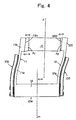
- Figs. 3 and 4 illustrate the operation state of the device at a low temperature such as room temperature and at a higher temperature than room temperature, respectively.
- the influence caused by such a temperature change will be larger according as the bonding area is smaller, because the distortion imposed upon the adhesive will be larger according as the bonding area is smaller. Therefore, according as the bonding area increases, the influence of the temperature variation will be smaller.
- fixing part 13 for fixing the device itself must support the combined mass of component H and the device itself. Therefore, if an impact is received, fixing part 13 is liable to be dismounted. If the length L2 of fixing part 13 is increased in order to increase the bonding area, the total length L1 of the device will also increase.
- an object of the present invention is to increase the displacement of each movable part and to sufficiently ensure the bonding between each mounting part and the component as well as the fixation of the device itself without changing the total length of the device and without reducing the bonding area at the joining surfaces of the mounting parts in a piezoelectric/electrostrictive device having such a form. Further, an object of the present invention is to firmly mount the component and the device in the case where the component is especially large and heavy or in the case where a large adhesive strength is needed.
- the present invention relates to a piezoelectric/electrostrictive device and a production method thereof, and is directed to a piezoelectric/electrostrictive device having a base including a pair of movable parts opposing each other and a fixing part that connects the movable parts with each other at one end thereof, wherein the piezoelectric/electrostrictive device has a piezoelectric/electrostrictive element disposed on at least one outside surface of the movable parts of the base.
- the piezoelectric/electrostrictive device is characterized in that the base includes a pair of long mounting parts disposed at the other end of the movable parts for mounting a component to be controlled or a component to be inspected, and the mounting parts extend for a predetermined length while holding slit-shaped gaps of a predetermined width along inside surfaces of the movable parts by being turned around at the other end of the movable parts.
- the fixing part constituting the base can be constructed to include a pair of slit-shaped gaps of a predetermined width disposed on the opposing sides of the fixing part and extending along the inside surfaces of the movable parts.
- the base is constructed with a ceramic laminate formed by laminating and calcining a plurality of ceramic green sheets in a large number, or can be constructed with a metal laminate formed by laminating and joining a plurality of metal plates in a large number, or can be constructed by bending one sheet of flat plate made of metal.
- the slit-shaped gaps between the movable parts and the mounting parts constituting the base and/or the slit-shaped gaps along the movable parts of the fixing part can be set to have a dimension that does not restrict a displacement of the movable parts during an operation of the piezoelectric/electrostrictive device.
- each mounting part and each movable part can be formed to have identical or approximately equal thicknesses.
- a component to be controlled or a component to be inspected is fixed onto inside surfaces of the movable parts constituting the base via an adhesive, and the piezoelectric/electrostrictive device can be used in a state in which the component to be controlled or the component to be inspected is sandwiched and held by the mounting parts.
- a more specific construction of the piezoelectric/electrostrictive device is a piezoelectric/electrostrictive device having a base including a pair of plate-shaped movable parts opposing each other, a fixing part that connects the movable parts with each other at one end thereof, and mounting parts connecting to the other end of the movable parts, the piezoelectric/electrostrictive device having a piezoelectric/electrostrictive element disposed on at least one outside surface of the movable parts constituting the base, characterized in that slit-shaped gaps intervene between the movable parts and the mounting parts, and a length L12 of the slit-shaped gaps is set to be larger than a length L5 of connecting parts that connect the movable parts to the mounting parts.
- the length L12 of the slit-shaped gaps is at least two times, preferably at least five times, as large as the length L5 of the connecting parts.
- the length L5 of the connecting parts and the length L12 of the slit-shaped gaps in the piezoelectric/electrostrictive device refer to the dimensions of the sites as defined in the piezoelectric/electrostrictive device shown in Fig. 21.
- a method of producing a piezoelectric/electrostrictive device is a method of producing a piezoelectric/electrostrictive device having a base including a pair of movable parts opposing each other, a fixing part that connects the movable parts with each other at one end thereof, and mounting parts that extend for a predetermined length while holding slit-shaped gaps of a predetermined width along inside surfaces of the movable parts by being turned around at the other end of the movable parts, wherein the piezoelectric/electrostrictive device has a piezoelectric/electrostrictive element disposed on at least one outside surface of the movable parts of the base.
- the first method of producing a piezoelectric/electrostrictive device according to the present invention is characterized in that a base block formed by laminating and calcining a large number of ceramic green sheets is adopted as a material for forming the base, and the base including the movable parts, the fixing part, and the mounting parts is formed by cutting the base block at a predetermined site along a lamination direction of the ceramic green sheets.
- the second method of producing a piezoelectric/electrostrictive device according to the present invention is characterized in that a flexible and bendable flat plate made of metal is adopted as a material for forming the base, and the base including the movable parts, the fixing part, and the mounting parts is formed by stamping the flat plate into a shape that delineates a planar development of the base so as to obtain a stamped structure, and bending the stamped structure at a predetermined site.
- the third method of producing a piezoelectric/electrostrictive device according to the present invention is characterized in that a base block formed by laminating and bonding a plurality of plates made of metal in a large number is adopted, and the base including the movable parts, the fixing part, and the mounting parts is formed by cutting the base block at apredetermined site along a lamination direction of the metal plates.
- each movable part constituting the base includes a long mounting part, whereby the joining surface of each mounting part is large and the area of bonding the component with each mounting part can be set to be large.
- the adhesive force of the component to the joining surface of each mounting part is strong, so that the component will not be easily dismounted from each mounting part, thereby making it possible to construct a joining structure that is strong against impact. Further, it is possible to prevent a situation in which the separation of the component from one mounting part causes damages of the other mounting part.
- each mounting part extends for a predetermined length while holding a slit-shaped gap of a predetermined width along the inside surface of each movable part by being turned around at the other end of the movable part. For this reason, a joining structure having a strong adhesive force between each mounting part and the component can be constructed without increasing the total length of the device and without degrading the displacement characteristics of the movable parts.
- this joining structure even if the component to be bonded to the mounting parts is large and has an increased mass to impose a large external force on the adhesive, a large bonding area can be ensured without increasing the total length of the device, so that the distortion per bonding area can be reduced. For this reason, according to the joining structure, the influence given to the device properties by the temperature change of the adhesive can be greatly restrained as compared with the case in which the bonding area is small, and the operation range in which the set device properties are exhibited in a stable state can be extended to a wide range from low temperature to high temperature.
- the area of the fixing part can be increased, without increasing the total length of the device, by increasing the length of the grooves.
- the bonding area that fixes the piezoelectric/electrostrictive device can be increased to provide a strong adhesive force, whereby the piezoelectric/electrostrictive device can be firmly fixed.
- the adhesive force can be sufficiently enhanced to stabilize the fixation of the device.
- a base constituting the piezoelectric/electrostrictive device As a base constituting the piezoelectric/electrostrictive device according to the present invention, it is possible to adopt a base (first base) constructed with a ceramic laminate formed by laminating and calcining a large number of ceramic green sheets, a base (second base) constructed by bending one sheet of flat plate made of metal, or a base (third base) constructed with a metal laminate formed by laminating and bonding a plurality of metal plates in a large number.
- the slit-shaped gaps between the movable parts and the mounting parts constituting the base are preferably set to have a slit width that does not restrict a displacement of the movable parts during an operation of the piezoelectric/electrostrictive device.
- each mounting part and each movable part constituting the base are preferably formed to have identical or approximately equal thicknesses.
- the base can be produced as follows.
- the first base can be produced with ease by adopting a base block obtained by lamination and calcination of a large number of ceramic green sheets as a material for forming the base, and using means for cutting the base block at a predetermined site along a lamination direction of the ceramic layers to form the base.
- the second base can be produced with ease by adopting a flexible and bendable flat plate made of metal as a material for forming the base, and stamping the flat plate into a shape that delineates a planar development of the base so as to obtain a stamped structure, and bending the stamped structure at a predetermined site to form the base.
- the third base can be produced with ease by adopting a flexible and bendable flat plate made of metal and adopting a base block formed by laminating and bonding a large number of the flat plates as a material for forming the base, and using means for cutting the base block at a predetermined site along a lamination direction to form the base.
- the piezoelectric/electrostrictive device can be used as active elements such as various transducers, various actuators, frequency region function components (filters), transformers, vibrators for communication or mechanical power, oscillators, and discriminators, as well as sensor elements for various sensors such as supersonic wave sensors, acceleration sensors, angular velocity sensors, impact sensors, and mass sensors.
- the piezoelectric/electrostrictive device can be suitably used as various actuators that are put to use for displacement, positioning adjustment, and angle adjustment mechanism for various precision components of optical instruments and precision apparatus.
- the piezoelectric/electrostrictive device according to the present invention is a concept used to encompass elements that convert electrical energy to mechanical energy and vice versa.
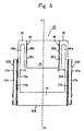
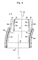
- Figs. 5 and 6 illustrate a first piezoelectric/electrostrictive device according to the present invention.
- the piezoelectric/electrostrictive device 10 is made of a base 10a and a pair of piezoelectric/electrostrictive elements 10b.
- Base 10a is formed by calcination of a laminate of ceramic green sheets.
- base 10a has a shape of an open-topped square whose one side is closed and whose other side is open.
- Base 10a is constructed with a pair of right and left movable parts 11, 12, a fixing part 13 that connects movable parts 11, 12 with each other at one endû ⁇ 1 ⁇ 2reof, and mounting parts 15, 16 that connect to the other end of movable parts 11, 12 via a connecting part 14.
- These parts 11 to 16 has an integrated structure composed of a ceramic structure.
- each of the movable parts 11, 12 constitutes an operating part by having a piezoelectric/electrostrictive element 10b adhere to an outside surface thereof.
- Fixing part 13 is fixed at its upper surface side or at its lower surface side, for example, by being bonded to gimbals of a suspension that holds a magnetic head of a hard disk drive.
- Magnetic head H for hard disk drive for example, which is a component to be controlled, is bonded and fixed to an inside surface of each of the mounting parts 15, 16.
- Mounting parts 15, 16 constituting the base 10a each extend for a predetermined length towards one end of movable parts 11, 12 along the inside surfaces of movable parts 11, 12 by being turned around at the other end of movable parts 11, 12 so as to hold slit-shaped gaps 15a, 16a of a predetermined width between mounting parts 15, 16 and inside surfaces of movable parts 11, 12.
- Mounting parts 15, 16 each extend approximately to a central part of movable parts 11, 12, and the inside surfaces thereof are formed to be joining surfaces 15b, 16b for bonding magnetic head H.
- the side surfaces of magnetic head H are bonded to the entire surface of joining surfaces 15b, 16b via adhesives 15c, 16c.
- An adhesive made of epoxy resin or the like is adopted as adhesives 15c, 16c so as to ensure a large bonding area.
- Slit-shaped gaps 15a, 16a between mounting parts 15, 16 and movable parts 11, 12 are set to have such a dimension that the displacement of movable parts 11, 12 is not restricted when piezoelectric/electrostrictive device 10 operates.
- slit-shaped gaps 15a, 16a are set to have an interval such that movable parts 11, 12 do not abut against mounting parts 15, 16 when movable parts 11, 12 are subjected to displacement operation. This prevents influence on the displacement properties of movable parts 11, 12 caused by mounting parts 15, 16 that are located on the inner surface side of movable parts 11, 12 and on the device characteristics caused by this.
- Piezoelectric/electrostrictive device 10 is in a state shown in Fig. 5 at the time of non-operation when a voltage is not applied to piezoelectric/electrostrictive element 10b.
- the longitudinal axis m (central axis of fixing part 13) of piezoelectric/electrostrictive device 10 is almost coincident with the central axis n of mounting parts 15, 16.
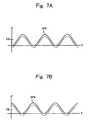
- a sinusoidal wave Wb having a predetermined bias voltage Vb is applied to a pair of electrodes 17a, 17b in one piezoelectric/electrostrictive element 10b, for example, as shown in the waveform diagram of Fig.
- a sinusoidal wave Wa having a phase different by approximately 180° from that of the sinusoidal wave Wb is applied to a pair of electrodes 17a, 17b in the other piezoelectric/electrostrictive element 10b, for example, as shown in Fig. 7B.
- the piezoelectric/electrostrictive layer 17c in the one piezoelectric/electrostrictive element 10b undergoes shrinking displacement in its principal surface direction.
- movable parts 11, 12 both displace in the illustrated right direction with respect to the longitudinal axis m of piezoelectric/electrostrictive device 10.
- the displacement amount of this displacement changes in accordance with the maximum value of the voltage applied to each piezoelectric/electrostrictive element 10b. The larger the maximum value of the voltage is, the large the displacement amount will be.
- piezoelectric/electrostrictive device 10 a minute displacement of piezoelectric/electrostrictive element 10b is amplified to become a large displacement operation by utilizing the deflection of movable parts 11, 12, and is transmitted to movable parts 11, 12.
- This makes it possible to displace mounting parts 15, 16 to a large extent with respect to the longitudinal axis m of piezoelectric/electrostrictive device 10, whereby position control of magnetic head H, for example, can be carried out accurately.
- piezoelectric/electrostrictive device 10 produces various conspicuous functions and effects such as described below, as compared with conventional piezoelectric/electrostrictive devices having this type of form. Namely, in piezoelectric/eiectrostrictive device 10, the area of bonding component H (for example, a magnetic head) can be set to a large value to greatly increase the bonding force without increasing the total length of the device, whereby the dislocation of component H from mounting parts 15, 16 and damages to mounting parts 15, 16 can be prevented.
- the area of bonding component H for example, a magnetic head
- the thickness of adhesives 15c, 16c that are allowed to intervene between component H and joining surfaces 15b, 16b of mounting parts 15, 16 can be decreased to greatly reduce the influence given to the device characteristics caused by the temperature change of adhesives 15c, 16c.
- the arm length (movable part bodies 11a, 12a) of movable parts 11, 12 can be set to a large value, whereby the maximum displacement amount of movable parts 11, 12 can be increased to improve the device characteristics.
- Fig. 1 that shows a conventional piezoelectric/electrostrictive device having this type of form
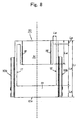
- Fig. 8 that shows a piezoelectric/electrostrictive device 10 according to one example of the present invention
- the same symbols represent the dimensional relationship of each site in the piezoelectric/electrostrictive device and the base.
- symbol L1 is the length of the device (which is also the total length of the base)
- symbol L2 is the length of the fixing part in the base
- symbol L3 is the length of the arm of the movable part in the base
- symbol L4 is the length of the joining surface of the mounting part in the base.
- Symbol L5 is the length of the connecting part which is a characteristic site of the piezoelectric/electrostrictive device according to the present invention
- symbol L6 is the interval of the slit-shaped gaps between the movable parts and the mounting parts, which gaps are characteristic sites of the piezoelectric/electrostrictive device according to the present invention.
- piezoelectric/electrostrictive device 10 according to the present invention can be confirmed to have excellent functions and effects such as described below, as compared with conventional piezoelectric/electrostrictive devices.
- the first one of the functions and effects produced by piezoelectric/electrostrictive device 10 is that the length L4 of the joining part to component H is extremely large, so that the bonding area to component H can be set to be large without increasing the total length L1 of the base.
- the adhesive force to component H is made considerably strong to prevent dislocation of component H from mounting parts 15, 16 and the damages to mounting parts 15, 16.
- the second one of the functions and effects produced by piezoelectric/electrostrictive device 10 is that, due to the length L4 of the joining part, the bonding area to component H can be set to a large value to increase the force of bonding component H, whereby the thickness of adhesives 15c, 16c that are allowed to intervene between component H and joining surfaces 15b, 16b of mounting parts 15, 16 can be decreased to greatly reduce the influence given to the device characteristics caused by the temperature change of adhesives 15c, 16c.
- the third one of the functions and effects produced by piezoelectric/electrostrictive device 10 is that the arm length L3 of movable parts 11, 12 and the length L4 of joining surfaces 15b, 16b of mounting parts 15, 16 can be set independently from each other.
- the arm length L3 of movable parts 11, 12, and the length L4 of joining surfaces 15b, 16b of mounting parts 15, 16 can be set to arbitrary large values to improve the device characteristics, and to strengthen the bonding force to component H to a greater extent.
- piezoelectric/electrostrictive device 10 if the component H to be used is short as shown in Fig. 9, adhesives 15c, 16c can be allowed to go around to one end surface side of component H to ensure a sufficient adhesive strength, and if component H has a cylindrical shape such as a cross section of an optical fiber as shown in Fig. 10, the gap between the outer perimeter of component H and mounting parts 15, 16 can be filled with adhesives 15c, 16c to ensure a sufficient adhesive strength.
- the production method is the first one of the production methods according to the present invention, and in this production method, each constituent member is defined as follows.
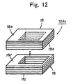
- the laminate shown in Fig. 12, which is obtained by laminating ceramic green sheets 18 shown in Fig. 11, is referred to as ceramic green laminate 10A1.
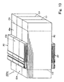
- the laminate shown in Fig. 13, which is obtained by calcining and integrating the ceramic green laminate 10A1, is referred to as ceramic laminate 10A2.
- the base shown in Fig. 14, in which mounting parts 15, 16, movable parts 11, 12 and fixing part 13 are integrated by cutting unnecessary portions from the ceramic laminate 10A2, is referred to as ceramic base 10a.
- the ceramic laminate 10A2 is eventually cut into chips in a form such that a plurality of piezoelectric/electrostrictive devices 10 are arranged in longitudinal and lateral directions in the same substrate, so as to produce piezoelectric/electrostrictive devices 10 in a large number in the same step; however, for simplicity of description, a method of producing one piezoelectric/electrostrictive device 10 will be described.
- ceramic powder such as zirconia is mixed with a binder, a solvent, a dispersant, a plasticizer, and the like by addition to prepare a slurry and, after the slurry is subjected to a defoaming treatment, a ceramic green sheet having a predetermined thickness is prepared by a method such as the reverse roll coater method or the doctor blade method.
- the ceramic green sheet is processed into various shapes and thicknesses by a method such as a stamping process using a mold or a laser process, so as to produce plural sheets of ceramic green sheets 18 shown in Fig. 11 for forming a base.
- These ceramic green sheets 18a to 18j are prepared to include at least plural sheets (for example, four sheets) of ceramic green sheets 18c, 18d, 18g, 18h having a window part k1 formed for forming a space between movable parts 11, 12, plural sheets (for example, seven sheets) of ceramic green sheets 18e to 18f having a window part k2 formed for forming mounting parts 15, 16 having joining surfaces 15b, 16b that are opposed to window part k1 for forming the space between movable parts 11, 12, plural sheets (for example, two sheets) of ceramic green sheets 18b, 18i in which a window part k3 that is to become slit-shaped gaps 15a, 16a is formed, and plural sheets (for example, two sheets) of ceramic green sheets 18a, 18j that are to become mov
- these ceramic green sheets 18 are laminated and press-bonded so that ceramic green sheets 18c to 18h, ceramic green sheets 18b, 18i, and ceramic green sheets 18e to 18f are sandwiched by ceramic green sheets 18a, 18j, so as to form ceramic green laminate 10A1, as shown in Fig. 12.
- the ceramic green sheets 18 are laminated by positioning ceramic green sheets 18e to 18f at the center.
- window part k2 a site appears to which a pressure is not applied at the time of press-bonding. Therefore, it is necessary to prevent generation of such a site by changing the order of lamination and press-bonding.
- the ceramic green laminate 10A1 is calcined to form ceramic laminate 10A2 shown in Fig. 13.
- the number of lamination times and the order of lamination for forming ceramic green laminate 10A1 are suitably changed in accordance with the set structure, so that a ceramic green laminate 10A1 having a set structure can be produced, for example, by suitably changing the shapes of window parts k1 to k3, the number of ceramic green sheets 18, or the like in accordance with the set structure.
- the shapes of window parts k1 to k3 can be determined in accordance with the desired functions, and the number of ceramic green sheets 18 and the thickness of each ceramic green sheet 18 are not specifically limited.
- the press-bonding of laminated ceramic green sheets 18 can provide an improved lamination property by addition of heat. Further, in laminating ceramic green sheets 18, a paste, a slurry, or the like containing ceramic powder and a binder as major components can be applied and printed on ceramic green sheets 18 to form a joining aid layer, whereby the lamination property at the interface of ceramic green sheets 18 can be improved.
- the ceramic powder it is preferable to use a ceramic powder having the same or similar composition as the ceramic used in ceramic green sheets 18. This can ensure the reliability of lamination of ceramic green sheets 18.
- ceramic green sheets 18a, 18j are small, it is preferable to handle them using a plastic film, particularly a polyethylene terephthalate film whose surface is coated with a silicone-series lubricant.
- a piezoelectric/electrostrictive element body (later-mentioned piezoelectric/electrostrictive element body 30) for forming piezoelectric/electrostrictive element 10b is formed on both surfaces of the obtained ceramic laminate 10A2, that is, on the surfaces formed by laminated ceramic green sheets 18a, 18j, as shown in Fig. 13.
- piezoelectric/electrostrictive element body 30 As a method for forming piezoelectric/electrostrictive element body 30, one can use a thick film forming method such as the screen printing method, the dipping method, the coating method, or the electrophoresis method, or a thin film forming method such as the ion beam method, the sputtering method, the vacuum vapor deposition method, the ion plating method, the chemical vapor deposition method (CVD), or the plating method.
- CVD chemical vapor deposition method
- piezoelectric/electrostrictive element body 30 it is preferable to use particularly a thick film forming method. This is because, if a thick film forming method is used for forming piezoelectric/electrostrictive layers 31 to 34, one can form a film by using a paste, a slurry, a suspension, an emulsion, or a sol containing piezoelectric ceramic particles or powder having an average particle size of from 0.01 to 5 ⁇ m, preferably from 0.05 to 3 ⁇ m, as a major component and, by calcining the formed film, one can obtain good piezoelectric/electrostrictive properties.
- the electrophoresis method for forming piezoelectric/electrostrictive element body 30 has an advantage of being capable of forming a film at a high density and with a high shape precision.
- the screen printing method is advantageous for simplification of the production process because one can carry out film forming and pattern forming at the same time.
- ceramic green laminate 10A1 is first calcined at a temperature of from 1200°C to 1600°C, and integrated to form ceramic laminate 10A2. Subsequently, electrode 36 of movable parts 11, 12 are printed and calcined at a predetermined position on both surfaces of ceramic laminate 10A2, and then piezoelectric/electrostrictive layer 34 is printed and calcined, and further the other electrode 35 is printed and calcined. This process is repeated for a predetermined number of times, and during this, a plurality of piezoelectric/electrostrictive layers 33 to 31 are formed in the same manner as piezoelectric/electrostrictive layer 34.
- terminals 37, 38 for electrically connecting electrodes 35, 36 to a driving circuit are printed and calcined.
- piezoelectric/electrostrictive element body 30 if materials are selected so that the temperature of calcining each member lowers in accordance with the order of lamination, for example, by using platinum (Pt) as one electrode 36, lead zirconate titanate (PZT) as piezoelectric/electrostrictive layers 31 to 34, gold (Au) as the other electrode 35, and silver (Ag) as terminals 37, 38, then, at each calcination stage, the resintering of the materials previously calcined does not occur, thereby avoiding generation of inconveniences such as exfoliation or agglomeration of electrode materials and others.
- platinum platinum
- PZT lead zirconate titanate
- Au gold
- Ag silver
- each member of piezoelectric/electrostrictive element body 30 and terminals 37, 38 can be successively printed and integrally calcined at a time. Also, after piezoelectric/electrostrictive layer 31 of the outermost layer is formed, electrode 35 or the like of the outermost layer can be disposed at a low temperature. Each member of piezoelectric/electrostrictive element body 30 and terminals 37, 38 do not necessarily need a heat treatment.
- piezoelectric/electrostrictive element body 30 In forming piezoelectric/electrostrictive element body 30, it is suitably carried out to form piezoelectric/electrostrictive element body 30 in advance on both surfaces of ceramic green laminate 10A1, that is, on each surface of ceramic green sheets 18a, 18j, and then ceramic green laminate 10A1 and piezoelectric/electrostrictive element body 30 are calcined at the same time.
- the calcination may be carried out on all the constituent films of ceramic green laminate 10A1 and piezoelectric/electrostrictive element body 30, or methods may be mentioned such that one electrode 36 and ceramic green laminate 10A1 are calcined at the same time or such that the other constituent films excluding the other electrode 35 and ceramic green laminate 10A1 are calcined at the same time.
- a method for simultaneously calcining piezoelectric element body 30 and ceramic green laminate 10A one can mention a method in which precursors of piezoelectric/electrostrictive layers 31 to 34 are molded by the tape molding method or the like using a slurry source material, then the precursors of piezoelectric/electrostrictive layers 31 to 34 before calcination are laminated on the surface of ceramic green laminate 10A1 by thermal press-bonding or the like, and calcined at the same time to prepare mounting parts 15, 16, movable parts 11, 12, piezoelectric/electrostrictive layers 31 to 34, and fixing part 13 at the same time.
- this method one must form electrode 36 in advance on the surface of ceramic green laminate 10A1 and/or piezoelectric/electrostrictive layers 31 to 34 by using the above-mentioned film forming method.
- the temperature for calcining the constituent films of piezoelectric/electrostrictive element body 30 is suitably determined by the materials constituting these films. Generally, the temperature is from 500°C to 1500°C and, for piezoelectric/electrostrictive layers 31 to 34, the temperature is preferably from 1000°C to 1400°C. In this case, in order to control the composition of piezoelectric/electrostrictive layers 31 to 34, it is preferable to sinter them in the presence of an evaporation source of the materials of piezoelectric/electrostrictive layers 31 to 34.
- Piezoelectric/electrostrictive element body 30 is not necessarily formed on both surfaces of ceramic laminate 10A2 or ceramic green laminate 10A1, so that it is of course possible to form piezoelectric/electrostrictive element body 30 on only one surface.
- piezoelectric/electrostrictive element body 30 instead of forming piezoelectric/electrostrictive element body 30 directly on ceramic laminate 10A2, one can form piezoelectric/electrostrictive element body 30 as a separate body by the previously mentioned method, and then cut it in an arbitrary manner to form piezoelectric/electrostrictive element 10b. Piezoelectric/electrostrictive element 10b thus formed can be stuck onto a previously formed base 10a with an adhesive such as an organic resin or glass for preparation.
- Ceramic laminate 10A2 having piezoelectric/electrostrictive element body 30 formed thereon is cut at a predetermined site to be formed into piezoelectric/electrostrictive device 10 according to the present invention.
- ceramic laminate 10A2 integral with piezoelectric/electrostrictive element body 30 along cutting lines C1, C2, C3 shown in Fig. 13, the side parts and the tip end parts of ceramic laminate 10A2 are excised.
- this excision forms piezoelectric/electrostrictive device 10 having mounting parts 15, 16 having joining surfaces 15b, 16b opposing each other in which ceramic base 10a and piezoelectric/electrostrictive element 10b are integrated.
- the timing for cutting ceramic laminate 10A2 and piezoelectric/electrostrictive element body 30 may be such that one may cut along cutting line C3 after cutting along cutting lines C1, C2 or one can cut along cutting lines C1, C2 after cutting along cutting line C3. Of course, these cuttings may be carried out at the same time. Further, the end surface of fixing part 13 opposing to cutting line C3 may be suitably cut as cutting line C4 at the time of, for example, precisely controlling the total length of the piezoelectric/electrostrictive device or the like.
- piezoelectric/electrostrictive device 10 having mounting parts 15, 16 having joining surfaces 15b, 16b opposing each other in which ceramic base 10a and piezoelectric/electrostrictive element 10b are integrated, thereby achieving simplification of the production process and improving the yield of piezoelectric/electrostrictive devices 10.
- the aforesaid production method is especially preferable in taking out piezoelectric/electrostrictive devices 10 in a large number in the same step by constructing the same substrate (integrated structure of ceramic laminate 10A2 and piezoelectric/electrostrictive element body 30) in such a manner that a plurality of piezoelectric/electrostrictive devices 10 are arranged both in the longitudinal direction and in the lateral direction.
- a mechanical process such as a dicing process or a wire-saw process, a laser beam process using laser such as YAG laser or excimer laser, or an electron beam process. In cutting out ceramic laminate 10A2, these processing methods are combined for processing.
- cutting lines C1, C2 shown in Fig. 13 are subjected to a wire-saw process, and cutting lines C3, C4 perpendicular to cutting lines C1, C2 (formation of end surfaces of fixing part 13 and mounting parts 15, 16) are subjected to dicing process.
- ceramic base 10a and piezoelectric/electrostrictive element 10b individually formed by cutting can be separately prepared, and these can be bonded to prepare piezoelectric/electrostrictive device 10.
- the materials of mounting parts 15, 16 and fixing part 13 constituting base 10a are not particularly limited as long as they have rigidity; however, it is preferable to use a ceramic to which the ceramic green sheet lamination method can be applied.
- a ceramic to which the ceramic green sheet lamination method can be applied.
- materials and others containing zirconia starting with stabilized zirconia and partially stabilized zirconia, alumina, magnesia, silicon nitride, aluminum nitride, or titanium oxide as a major component may be mentioned.
- materials containing a mixture of these as a major component may be mentioned.
- materials containing zirconia, particularly stabilized zirconia, as a major component, and materials containing partially stabilized zirconia as a major component are preferable.
- movable parts 11, 12 constituting base 10a are parts that are driven by displacement of piezoelectric/electrostrictive element 10b.
- Movable parts 11, 12 are flexible members shaped like a thin plate, and have a function of amplifying the extending and shrinking displacement of piezoelectric/electrostrictive element 10b disposed on the surface as a bending displacement, and transmits the displacement to mounting parts 15, 16. Therefore, it is sufficient that the shape or the material quality of movable parts 11, 12 are flexible and have mechanical strength of a degree that will not be broken by bending deformation, so that the materials can be suitably selected in consideration of the responsiveness and operability of mounting parts 15, 16.
- the thickness L10 of movable parts 11, 12 is preferably about 2 ⁇ m to 100 ⁇ m, and the combined thickness of movable parts 11, 12 and piezoelectric/electrostrictive element 10b is preferably from 7 ⁇ m to 500 ⁇ m.
- the thickness of electrodes 35, 36 is preferably from 0.1 ⁇ m to 50 ⁇ m, and the thickness of piezoelectric/electrostrictive layers 31 to 34 is preferably from 3 ⁇ m to 300 ⁇ m.
- materials constituting movable parts 11, 12 one can suitably use ceramics similar to mounting parts 15, 16 and fixing part 13.
- materials containing zirconia, particularly stabilized zirconia, as a major component, and materials containing partially stabilized zirconia as a major component are most suitably used because of having a large mechanical strength, having a high toughness, and having a small reactivity with the piezoelectric/electrostrictive layers or the electrode materials, though being thin.
- stabilized zirconia and partially stabilized zirconia those that are stabilized or partially stabilized in the following manner are preferable. Namely, as the compounds that stabilize or partially stabilize zirconia, there are yttrium oxide, ytterbium oxide, cerium oxide, calcium oxide, and magnesium oxide. Intended stabilization of zirconia is possible by adding at least one of the compounds and allowing the compound to be contained, or by not only adding only one kind of compound but also adding these compounds in combination.
- the amount of addition of each compound is from 1 to 30 mol%, preferably from 1.5 to 10 mol%, in the case of yttrium oxide or ytterbium oxide; from 6 to 50 mol%, preferably 8 to 20 mol%, in the case of cerium oxide; and from 5 to 40 mol%, preferably from 5 to 20 mol% in the case of calcium oxide or magnesium oxide.
- an additive such as a sintering aid
- alumina, silica, transition metal oxide, and others within a range of from 0.05 to 20 wt%; however, if calcining integration by the film forming method is adopted as a technique for forming piezoelectric/electrostrictive element 10b, it is also preferable to add alumina, magnesia, transition metal oxide, and others as additives.
- the average crystal grain size of zirconia is preferably from 0.05 to 1 ⁇ m.
- movable parts 11, 12 one can use ceramics similar to mounting parts 15, 16 and fixing part 13; however, it is advantageous in obtaining reliability of the joining part, strength of piezoelectric/electrostrictive device 10, and reduction of the cumbersomeness of the structure to construct movable parts 11, 12 preferably with substantially the same material.
- Fig. 15 shows a modified example in which the first piezoelectric/electrostrictive device 10 is modified.
- slit-shaped gaps 13a, 13b opposing to gaps 15a, 16a are disposed at the site of the fixing part 13 constituting base 10a on the side of movable parts 11, 12.
- Rear wall portions of slit-shaped gaps 15a, 16a and slit-shaped gaps 13a, 13b are each filled with elastic members 19a, 19b made of resin.
- Piezoelectric/electrostrictive device 10A is intended to cope with the impact from outside of movable parts 11, 12 opposing to mounting parts 15, 16 via slit-shaped gaps 15a, 16a.
- the stress concentrated on connecting part 14 of movable parts 11, 12 and fixing parts 15, 16 is dispersed and absorbed by elastic members 19a, 19b, thereby improving the impact resistance of movable parts 11, 12 caused by the stress concentration at the connecting part 14.
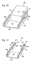
- Figs. 16 and 17 show a piezoelectric/electrostrictive device 20 according to the second embodiment of the present invention.
- Piezoelectric/electrostrictive device 20 is composed of a base 20a and a pair of piezoelectric/electrostrictive elements 20b.
- Base 20a is constructed by bending one sheet of flat plate made of metal.
- base 20a is constructed with a pair of right and left movable parts 21, 22, a fixing part 23 that connects movable parts 21, 22 with each other at one end thereof, and a pair of mounting parts 25, 26 that connect to the other end of movable parts 21, 22 via a connecting part 24.
- These sites 21 to 26 are integrally formed with one sheet of flat plate made of metal, and piezoelectric/electrostrictive element 20b is the same as piezoelectric/electrostrictive element 10b constituting the first piezoelectric/electrostrictive device 10 according to the first embodiment.
- each of the movable parts 21, 22 constitutes an operating part by having a piezoelectric/electrostrictive element 20b adhere to an outside surface thereof.
- Fixing part 23 is fixed at its lower surface side, for example, by being bonded to gimbals of a suspension that holds a magnetic head of a hard disk drive.
- Magnetic head H for hard disk drive for example, which is a component to be controlled, is bonded and fixed to an inside surface of each of the mounting parts 25, 26.
- Each of movable parts 21, 22 constituting base 20a shows a narrow flat-plate shape erected by being bent from the side peripheries of flat-plate-shaped fixing part 23, and extends over fixing part 23 for a predetermined length towards the other end.
- Mounting parts 25, 26 are integral with movable parts 21, 22 via connecting part 24, and each extend for a predetermined length towards the one end along the inside surfaces of movable parts 21, 22 by being turned around at the other end of movable parts 21, 22 so as to hold slit-shaped gaps 25a, 26a of a predetermined width between mounting parts 25, 26 and inside surfaces of movable parts 21, 22.
- Mounting parts 25, 26 each extend approximately to a central part of movable parts 21, 22, and the inside surfaces thereof are formed to be joining surfaces 25b, 26b for bonding magnetic head H.
- the side surfaces of magnetic head H are bonded to the entire surface of joining surfaces 25b, 26b via adhesives in the same manner as in piezoelectric/electrostrictive device 10.
- An adhesive made of epoxy resin or the like is adopted as the adhesives so as to ensure a large bonding area.
- Piezoelectric/electrostrictive device 20 is substantially the same as piezoelectric/electrostrictive device 10 in that the base 20a constituting piezoelectric/electrostrictive device 20 includes mounting parts 25, 26 that extend for a predetermined length towards the one end along the inside surfaces of movable parts 21, 22 by being turned around at the other end of movable parts 21, 22, and mounting parts 25, 26 hold slit-shaped gaps 25a, 26a of a predetermined width between mounting parts 25, 26 and inside surfaces of movable parts 21, 22, and in that the inside surfaces of mounting parts 25, 26 are formed to be joining surfaces 25b, 26b for bonding component H, whereby piezoelectric/electrostrictive device 20 operates in the same manner and produces similar functions and effects as piezoelectric/electrostrictive device 10.
- base 20a constituting piezoelectric/electrostrictive device 20 according to the second embodiment of the present invention is formed by the second production method according to the present invention, as will be described below.
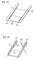
- Base 20a constituting piezoelectric/electrostrictive device 20 according to the second embodiment of the present invention is formed by using an original base plate 20A shown in Fig. 18.
- Original base plate 20A is formed by stamping a flat plate made of metal into a shape that delineates a planar development of base 20a, and original base plate 20A is bent along two-dotted chain lines E1, E2, E3 shown in Fig. 18.
- Original base plate 20A is formed into base 20a composed of movable parts 21, 22, fixing part 23, connecting part 24, and mounting parts 25, 26 by this bending process.
- base 20a slit-shaped gaps 25a, 26a are ensured between movable parts 21, 22 and mounting parts 25, 26.
- a piezoelectric/electrostrictive element 20b is stuck via an adhesive onto the outside surfaces of movable parts 21, 22 in base 20a thus prepared by bending, thereby to form piezoelectric/electrostrictive device 20.
- piezoelectric/electrostrictive elements 10a, 20a constituting the first piezoelectric/electrostrictive device 10 and the second piezoelectric/electrostrictive device 20; however, piezoelectric/electrostrictive element 30A developed by the applicant of the present invention and shown in Fig. 20 is adopted in each of piezoelectric/electrostrictive devices 10, 20.
- the piezoelectric/electrostrictive layer has a four-layer structure, and is constructed with piezoelectric/electrostrictive layers 31, 32, 33, 34, first and second electrodes 35, 36 that intervene between and surround these piezoelectric/electrostrictive layers, and a pair of terminals 37, 38.
- Piezoelectric/electrostrictive element 30A corresponds to the one cut out by cutting piezoelectric/electrostrictive element body 30 shown in Fig. 13.
- piezoelectric ceramic is used in piezoelectric/electrostrictive layers 31 to 34 constituting piezoelectric/electrostrictive element 30A
- electrostrictive ceramic ferroelectric ceramic, antiferroelectric ceramic, or the like
- ferroelectric ceramic ferroelectric ceramic
- antiferroelectric ceramic or the like
- lead zirconate As a material for forming piezoelectric/electrostrictive layers 31 to 34, one can specifically mention lead zirconate, lead titanate, magnesium lead niobate, zinc lead niobate, manganese lead niobate, antimony lead stannate, manganese lead tungstate, cobalt lead niobate, barium titanate, bismuth sodium titanate, potassium sodium niobate, strontium bismuth tantalate, which are used alone or as a suitable mixture thereof.
- a material containing lead zirconate, lead titanate, or magnesium lead niobate as a major component or a material containing bismuth sodium titanate as a major component is suitable.
- the characteristics of the piezoelectric/electrostrictive layers can be adjusted by adding a suitable material to the materials for forming piezoelectric/electrostrictive layers 31 to 34.
- a suitable material to be added one can mention oxides of lanthanum, calcium, strontium, molybdenum, tungsten, barium, niobium, zinc, nickel, manganese, cesium, cadmium, chromium, cobalt, antimony, iron, yttrium, tantalum, lithium, bismuth, or tin, or materials that eventually become oxides, which are used alone or as a suitable mixture thereof.
- the coercive electric field or the piezoelectric property can be adjusted.
- Electrodes 35, 36 constituting piezoelectric/electrostrictive elements 30A are preferably made of a metal material that is solid at room temperature and excellent in electrical conductivity.
- a metal material one can mention metals such as aluminum, titanium, chromium, iron, cobalt, nickel, copper, zinc, niobium, molybdenum, ruthenium, palladium, rhodium, silver, tin, tantalum, tungsten, iridium, platinum, gold, or lead, which are used as a single metal or an alloy of these metals .
- a thermet material obtained by dispersing ceramics made of the same materials as or made of different materials from the piezoelectric/electrostrictive layers into these metal materials.
- Piezoelectric/electrostrictive element 30A is preferably formed by integrally calcining piezoelectric/electrostrictive layers 31 to 34 and electrodes 35, 36 in a mutually laminated state.
- electrodes 35, 36 it is preferable to adopt those made of a high-melting-point metal material such as platinum, palladium, or an alloy of these, or an electrode made of a thermet material which is a mixture of a high-melting-point metal material and the materials for forming piezoelectric/electrostrictive layers 31 to 34 or other ceramic materials.
- the thickness of electrodes 35, 36 preferably has a film shape as thin as possible because the thickness becomes a factor that affects the displacement of piezoelectric/electrostrictive element 30. For this reason, in order that the electrodes formed by being integrally calcined with piezoelectric/electrostrictive layers 31 to 34 have a film shape as thin as possible, it is preferable to use the material for forming electrodes 35, 36 in a form of a metal paste, for example, a gold resinate paste, platinum resinate paste, silver resinate paste, or the like.
- the thickness of piezoelectric/electrostrictive element 30A is preferably within a range from 40 ⁇ m to 180 ⁇ m if piezoelectric/electrostrictive element 30A is to be used as piezoelectric/electrostrictive elements 10b, 20b of piezoelectric/electrostrictive devices 10, 20 according to each embodiment. If the thickness is below 40 ⁇ m, piezoelectric/electrostrictive element 30A is liable to be broken during the handling, whereas if the thickness exceeds 180 ⁇ m, the scale reduction of the device will be difficult.
- the piezoelectric/electrostrictive element by allowing the piezoelectric/electrostrictive element to have a multi-layer structure such as in piezoelectric/electrostrictive element 30, one can increase the output of piezoelectric/electrostrictive element to enlarge the displacement of the device. Furthermore, by allowing the piezoelectric/electrostrictive element to have a multi-layer structure, the rigidity of the device will be improved, thereby advantageously raising the resonance frequency of the device to increase the speed of the displacement operation of the device.
- Piezoelectric/electrostrictive element 30A is prepared using means for cutting an original plate of a large area such as piezoelectric/electrostrictive element 30, which is formed by laminating and calcining piezoelectric/electrostrictive layers 31 to 34 and electrodes 35, 36 by printing or tape molding, cut into a predetermined dimension in a large number with the use of a dicing machine, a slicer, a wire-saw, or the like.
- Piezoelectric/electrostrictive element 30A is thinner and has a lower hardness than a ceramic base, so that the speed of cutting the original plate can be set to be high, whereby the original plates can be processed in a large mass and at a high speed.
- Piezoelectric/electrostrictive element 30A has a simple plate-shaped structure and can be easily handled with. Also, since the surface area is small, the amount of adhering dust is small, and the stains can be easily removed. However, since piezoelectric/electrostrictive element 30A is mainly made of a ceramic material, a suitable cleaning condition must be set in supersonic cleaning. In piezoelectric/electrostrictive element cut out from the original plate, it is preferable to perform a precision cleaning treatment by US cleaning and then perform a heat treatment at 100°C to 1000°C in atmospheric air so as to completely remove the moisture and organic substances that have penetrated into fine pores of the ceramic material.
- piezoelectric/electrostrictive element 30A is to be adopted as piezoelectric/electrostrictive elements 10b, 20b constituting piezoelectric/electrostrictive devices 10, 20 according to each embodiment, it is preferable to use a resin-series adhesive such as epoxy resin, UV resin, or hot-melt adhesive, or an inorganic adhesive such as glass, cement, solder, or brazing material as a bonding means to the base of each piezoelectric/electrostrictive element 30A. Also, a mixture of resin-series adhesive with metal powder or ceramic powder can be used as well. The hardness of the adhesive is preferably not less than 80 in terms of Shore hardness D.
- the bonding site it is preferable to perform a surface roughening treatment such as blasting, etching, or plating on the site of the surface of the base where piezoelectric/electrostrictive element 30A is to be bonded.
- a surface roughening treatment such as blasting, etching, or plating
- the surface roughness of the bonding site it is preferable to perform a surface roughening treatment such as blasting, etching, or plating on the site of the surface of the base where piezoelectric/electrostrictive element 30A is to be bonded.
- the surface of the bonding site on the piezoelectric/electrostrictive element side is preferably rough as well. If one wishes that the electrodes are not electrically conducted to the base, the electrodes are not disposed on the surface of the piezoelectric/electrostrictive layer
- solder or brazing material is to be used as the adhesive, it is preferable to dispose an electrode layer made of a metal material on the surface of the piezoelectric/electrostrictive element in order to improve the wettability.
- the thickness of the adhesive is preferably within the range from 1 ⁇ m to 50 ⁇ m.
- the thickness of the adhesive is preferably small in view of reducing variations in the displacement and in the resonance characteristics of the device and in view of saving space; however, in order to ensure the characteristics such as adhesive strength, displacement, and resonance, the optimal thickness is set for each adhesive to be adopted.
- the piezoelectric/electrostrictive element In bonding the piezoelectric/electrostrictive element to the base, the piezoelectric/electrostrictive element is bonded to the base so that the piezoelectric/electrostrictive element completely overlaps the bending position of the fixing part while allowing the electrodes of the piezoelectric/electrostrictive element to be on the side of the fixing part of the base.
- the piezoelectric/electrostrictive element is preferably bonded so as to align with the end of the base on the fixing part side; however, in order to facilitate the connection between the terminals of the piezoelectric/electrostrictive element and the external terminals, one may bond the piezoelectric/electrostrictive element to protrude outward from the end of the base.
- the piezoelectric/electrostrictive element is liable to be broken as compared with the base which is made of metal, one must take care in handling the piezoelectric/electrostrictive element. After the piezoelectric/electrostrictive element is stuck onto a predetermined position of the base with an adhesive, a cutting and cleaning process is carried out to produce the device.
- the piezoelectric/electrostrictive device according to the third embodiment of the present invention is obtained by replacing ceramic with metal in the base having the same shape as base 10a constituting the first piezoelectric/electrostrictive device 10, where the base material is changed from ceramic to metal in forming the base. Further, in the production of the piezoelectric/electrostrictive device, the third production method according to the present invention is adopted.
- metal plates are prepared instead of the ceramic green sheets in the first production method.
- the base is prepared.
- bonding means one can adopt bonding, brazing, soldering, diffusion-joining, supersonic joining, thermal press-bonding, cladding method or the like using an adhesive such as organic resin or glass. Further, one can adopt means for integrating the laminated metal plates by welding or the like.
- each metal plate to be laminated For preparation of the window part of each metal plate to be laminated, one can adopt laser processing, electric discharge machining, etching, sand-blasting, or the like in addition to stamping with a mold.
- the material of the metal plates constituting the base one can adopt the same material as the material of base 20a of piezoelectric/electrostrictive device 20.
- the material constituting the base as the material constituting the base, one can use metal plates and ceramic plates in combination, and this can form a base having a hybrid structure.
- resin as the material constituting the base to form a base made of resin and, depending on the usage of the piezoelectric/electrostrictive device, one can construct a piezoelectric/electrostrictive device having a base made of resin as a constituent member.
- the number of times for bonding and the order of bonding for laminating and integrating the metal plates are by no means limited, and the number of sheets, the shape, the thickness, and others of the metal plates are suitably determined in accordance with the set structure.
- a carbon material or a resin material in place of metal plates if the bonding method or the material does not raise a problem.
- piezoelectric/electrostrictive element 30A1 for the piezoelectric/electrostrictive element to be used, one can adopt a piezoelectric/electrostrictive element 30A1 in the same manner as piezoelectric/electrostrictive elements 10b, 20b of piezoelectric/electrostrictive devices 10, 20.
- a cutting and cleaning process can be carried out to produce the piezoelectric/electrostrictive device.
- the piezoelectric/electrostrictive element is preferably constructed with at least four layers. Further, the piezoelectric/electrostrictive element is preferably constructed with at most 10 layers.
- the piezoelectric/electrostrictive element is preferably prepared by the printing multi-layer method.
- the positional shift of the electrodes of the piezoelectric/electrostrictive element is preferably below 50 ⁇ m. If the number of layers of the piezoelectric/electrostrictive layers is increased, the driving power can be enhanced; however, in accordance therewith, the power consumption increases. Therefore, in practically carrying out the process, one may determine the number of layers suitably in accordance with the usage. It is preferable to produce the piezoelectric/electrostrictive element by a method of forming a film such as a thin film or a thick film.
- the base In constructing the base with a metal material, it is preferable to adopt a cold-calendered metal plate at least in the movable parts.
- a piezoelectric/electrostrictive device 10 according to the first embodiment of the present invention is prepared, and Fig. 21 shows the dimensional relationship of piezoelectric/electrostrictive device 10 and each site of component H.
- Symbols L of the same series in piezoelectric/electrostrictive device 10 each denote the length L1 of the device (total length of the base), the length L2 of the fixing part in the base, the length L3 of the arm of the movable parts in the base, the length L4 of the joining surface of the mounting parts in the base, the length L5 of the connecting part, the interval L6 of the slit-shaped gaps between the movable parts and the mounting parts, the interval L7 between the two movable parts, the interval L8 between the two mounting parts, the thickness L9 of the mounting parts, the thickness L10 of the movable parts, the height L11 of the movable parts (the distance in the front-and-back direction of the document sheet), and the length L12 of the slit-
- the relationship between the interval L8 of the mounting parts and the lateral length M4 of the piezoelectric/electrostrictive device is such that L8 ⁇ M4, more preferably L8 - M4. If L8 ⁇ M4, it is necessary to enlarge the gap between the two mounting parts in inserting component H, and there is a fear of breaking the device in enlarging the gap between the two mounting parts.
- the thickness M6 of the adhesive is from 0.1 to 0.005 mm, preferably from 0.05 to 0.01 mm. If the thickness of the adhesive is larger than 0.1 mm, there will be a large influence of the temperature on the displacement of the two movable parts at a high temperature.
- the thickness M6 of the adhesive is set to be smaller than 0.01 mm, variations are liable to occur in the adhesive strength to component H. Therefore, the thickness M6 of the adhesive is more preferably from 0.01 to 0.03 mm.
- the relationship between the length L5 of the connecting part and the thickness L10 of the movable parts is such that L5 ⁇ L10
- the relationship between the length L5 of the connecting part and the thickness L9 of the mounting parts is such that L5 ⁇ L9.
- the connecting part is a site that connects the movable parts to the mounting parts, and is structurally the weakest site. Therefore, if the length L5 of the connecting part does not satisfy these relationships, the connecting part becomes liable to be broken.
- the relationship between the longitudinal length M5 of component H and the length L4 of the joining surfaces of the mounting parts is such that M5 ⁇ L4.
- the joining surfaces of the mounting parts function so as to ensure the adhesive strength to component H, and it makes no sense if the length L4 of the joining surfaces of the mounting parts is made longer than the longitudinal length M5 of component H.
- the component to be adopted has a different shape from that of component H, for example, if it is a component having a shape shown in Figs. 8 and 9, this does not apply.
- the interval L6 of the slit-shaped gaps (slit gaps) between the movable parts and the mounting parts is from 0.2 to 0.001 mm, preferably from 0.1 to 0.01 mm, more preferably from 0.07 to 0.03 mm. If the interval L6 of the slit gaps is below 0.001 mm, the movable parts are brought into contact with the mounting parts at the time of high displacement of the movable parts, thereby to restrict the displacement operation of the movable parts. Further, if the interval L6 of the slit gaps is larger than 0.2 mm, the total lateral width M1 of the device will be larger, which is meaningless.
- the injected adhesive is liable to go around into the slit gaps to fill the slit gaps. If the interval L6 of the slit gaps is larger than 0.03 mm, the going around of the adhesive into the slit gaps is restrained.
- piezoelectric/electrostrictive device 10 can have a mode of having a stopper function against the impact from the outside of the movable parts by utilizing the abutment of the movable parts to the mounting parts at the time of,high displacement operation of the two movable parts.
- the length L12 of the slit-shaped gaps is set to be at least two times, preferably at least five times, as large as the length L5 of the connecting part. This allows that, even if the length M5 of component H cannot be made equal to the length L4 of the mounting parts, that is, even if M5 > L4, the bonding area to component H can be set to be large to ensure an adhesive strength, and also the length L3 of the arm of the movable parts can be set to be large to ensure a large displacement.
- the thickness L9 of the mounting parts is from 0.2 to 0.11 mm, preferably from 0.1 to 0.02 mm, more preferably from 0.07 to 0.03 mm. If the thickness L9 of the mounting parts exceeds 0.2 mm, the total width M1 of the device will be disadvantageously large, whereas if the thickness L9 of the mounting parts is below 0.01 mm, the device is liable to be broken.
- the thickness L10 of the movable parts is from 0.2 to 0.001 mm, preferably from 0.1 to 0.01 mm, more preferably from 0.08 to 0.03 mm.
- the length L2 of the fixing part, the arm length L3 of the movable parts, the length L5 of the connecting part, the interval L6 of the slit gaps, the thickness L9 of the mounting parts, the thickness L10 of the movable parts, and the thickness M6 of the adhesive are preferably as small as possible. This reduces the total length L1 and the total width M1 of the device.
- the arm length L3 of the movable parts is from 0.2 to 3 mm, preferably from 0.3 to 2 mm.
- the length L4 of the joining surfaces of the mounting parts is from 0.05 to 2 mm.
- the interval L7 between the two movable parts is from 0.1 to 2 mm, preferably from 0.2 to 1.6 mm.
- the thickness L9 of the mounting parts is from 0.002 to 0.1 mm, preferably from 0.01 to 0.08 mm.
- the height L11 of the movable parts is from 0.05 to 2 mm, preferably from 0.1 to 0.5 mm.
- the thickness M3 between the mounting parts and the piezoelectric/electrostrictive element is from 0.0007 to 0.5 mm.
- the ratio of the arm length L3 of the movable parts to the interval L7 between the two movable parts is from 0.5 to 10, preferably from 0.5 to 5.
- the ratio of the interval L7 between the two movable parts to the thickness L10 of the movable parts is from 0.5 to 20, preferably from 1 to 15, more preferably from 1 to 10.
- the thickness L10 of the movable parts and the height L11 of the movable parts satisfy a relationship of L10 ⁇ L11.
- the thickness L10 of the movable parts and the length M2 by which the end of the substantial driving part of the piezoelectric/electrostrictive element overlaps with the fixing part satisfy a relationship of M2 > (L10)/2.
- This Example is a modified example in which the first piezoelectric/electrostrictive device 10 according to the present invention is modified, where a piezoelectric/electrostrictive device 10B is prepared in which the base has a form corresponding to the base of the piezoelectric/electrostrictive device shown in Fig. 15.
- the dimensional relationship of the sites of piezoelectric/electrostrictive device 10B is shown in Fig. 22.
- Symbols L of the same series in piezoelectric/electrostrictive device 10B are the same as those in piezoelectric/electrostrictive device 10 formed in Example 1; however, the dimensions of some of the sites and the dimension of the sites of component H are omitted.
- the width L13 of the slit-shaped gaps of the fixing part is from 0.2 to 0.001 mm, preferably from 0.1 to 0.01 mm, more preferably from 0.07 to 0.03 mm.
- the length L14 of the slit-shaped gaps of the fixing part can be a length till the fixing part interferes with component H, and is preferably from 0.05 to 2 mm, more preferably from 0.1 to 0.5 mm.
- the dimensions of the other sites are set to be the same dimensions as in piezoelectric/electrostrictive device 10 prepared in Example 1.
Landscapes
- Engineering & Computer Science (AREA)
- Manufacturing & Machinery (AREA)
- Chemical & Material Sciences (AREA)
- Inorganic Chemistry (AREA)
- General Electrical Machinery Utilizing Piezoelectricity, Electrostriction Or Magnetostriction (AREA)
Abstract
An object of the present invention is to enhance the adhesive
force of bonding a component H to one ends of a pair of right
and left movable parts 11, 12 of a piezoelectric/electrostrlctive
device, wherein the piezoelectric/electrostrictive device has
a base 10a including the movable parts 11, 12 and a fixing part
13 on the other ends thereof, and a
piezoelectric/electrostrictive elements 10b, 10b on the side
surfaces of movable parts 11, 12 of base 10a. Base 10a
constituting the piezoelectric/electrostrictive device has a
pair of long
mounting parts 15, 16 for mounting component H on the other end
of movable parts 11, 12. Mounting parts 15, 16 extend for a
predetermined length while holding slit-shaped gaps 15a, 16a
of a predetermined width along the inside surfaces of movable
parts 11, 12 by being turned around at the other end of movable
parts 11, 12. This increases the bonding area of mounting parts
15, 16 to component H, thereby greatly improving the adhesive
force of bonding the component.
Description
The present invention relates to a
piezoelectric/electrostrictive device of a form such that the
displacement operation of a piezoelectric/electrostrictive
element is transmitted to a pair of right and left movable parts
to control a component to be controlled, which component is
sandwiched and held by the other ends of the movable parts, or
the displacement operation of a pair of right and left movable
parts that sandwich and hold a component to be inspected on the
other end is sensed by a piezoelectric/electrostrictive element
to sense the characteristics of the component to be inspected.
Referring to Fig. 1, a conventional
piezoelectric/electrostrictive device having such a form is
constructed in such a manner that a
piezoelectric/electrostrictive element 10b is disposed on each
of the outside surfaces of a pair of right and left movable parts
11, 12 constituting abase 10a. Movable parts 11, 12 are connected
with each other by means of a connecting part 13 on one end thereof,
and movable part bodies 11a, 12a extend towards the other end
thereof. The other end of movable part bodies 11a, 12a are made
into mounting parts 11b, 12b for mounting a component H such
as a component to be controlled or a component to be inspected.
In a piezoelectric/electrostrictive device having such
a form, if component H to be mounted is long in the longitudinal
direction of the device, onemust increase the length L4 of mounting
parts 11b, 12b, as shown in Fig. 2. In this case, the total length
L1 of the device is elongated by the amount of increase in the
length L4 of mounting parts 11b, 12b. Thus, if the length h of
component H to be mounted is equal to the length L4 of mounting
parts 11b, 12b, the total length L1 of the device is restricted
by the length h of component H.
On the other hand, in the case of mounting a long component
H shown in Fig. 2 to mounting parts 11b, 12b, if the length L4
of mounting parts lib, 12b are, for example, let as it is shown
in Fig. 1 without being changed, the total length L1 of the device
is unchanged irrespective of the length h of component H. However,
in this case, the length L4 of mounting parts 11b, 12b will be
shorter than the length h of component H, thereby decreasing
the area of the joining surface (bonding area) on component H.
Therefore, if an ordinary adhesive made of resin is used as
adhesives h1, h2, the adhesive strength on component H decreases.
Decrease in the adhesive strength on component H in the worst
cases causes component H to be dismounted from mounting parts
11b, 12b.
A component H having a large dimension h in the longitudinal
direction will have a mass that is increased by the amount of
elongation of the length h if the other dimensions and the density
thereof remain unchanged. Therefore, if the bonding area is small,
for example, if mounting parts 11b, 12b are each in a state shown
in Fig. 1, the impact imposed upon each of the adhesives h1,
h2 will be large, whereby component H is more liable to be
dismounted from each of mounting parts 11b, 12b.
In a piezoelectric/electrostrictive device having such
a form, if component H is dismounted from one of mounting parts
11b, 12b, the other of mounting parts 11b, 12b must support
component H to succeed receiving the impact applied to component
H. In this state, component H is liable to be dismounted from
the other mounting part, and also there is a fear that the
supporting balance of the mounted state may be lost to cause
the one supporting mounting part or the movable part connected
thereto to be broken by the action of torsional force.
In order to meet this problem, one must use an adhesive
having an extremely high adhesive strength; however, it is
generally difficult to obtain a special adhesive that can ensure
a sufficient adhesive strength no matter how small the bonding
area is. Furthermore, there is naturally a limit even in the
case of Using an adhesive having such a special property.
In a piezoelectric/electrostrictive device having such
a form, in the case of improving the device properties by increasing
the displacement of mounting parts 11b, 12b, one must increase
the amount of displacement of the movable part bodies 11a, 12a
by increasing the length of the movable part bodies 11a, 12a
of movable parts 11, 12. However, in order to increase the length
of the movable part bodies 11a, 12a of movable parts 11, 12 without
increasing the total length L1 of the device, one must reduce
the length of mounting parts 11b, 12b. As a result of this, the
bonding area of joining surfaces 11b1, 12b1 at the mounting parts
11b, 12b will be smaller to weaken the adhesive force of component
H to joining surfaces 11b1, 12b1 of mounting parts 11b, 12b all
the more, whereby component H will be more liable to be dismounted
and drop off from joining surfaces 11b1, 12b1.
In a piezoelectric/electrostrictive device having such
a form, in order to mount component H onto mounting parts 11b
12b of movable parts 11, 12, component H is bonded to joining
surfaces 11b1, 12b1 generally through the intermediary of
adhesives h1, h2 made of resin. However, adhesives h1, h2 made
of resin will have a reduced hardness or reduced Young's modulus
when the temperature changes above room temperature. The
temperature change of the state of use of
piezoelectric/electrostrictive devices is, for example, of a
degree within a range from room temperature to 100°C. However,
even in this temperature range, adhesives h1, h2 will be softened
at a high temperature. For this reason, the distortion of
adhesives h1, h2 when an external force is applied will differ
greatly between the state of room temperature and the state of
higher temperature than this. Therefore, the device properties
of the piezoelectric/electrostrictive device having this form
will differ greatly at a state of high temperature, even though
the device properties in a state of room temperature remain as
originally set.
Figs. 3 and 4 illustrate the operation state of the device
at a low temperature such as room temperature and at a higher
temperature than room temperature, respectively. The influence
caused by such a temperature change (temperature variation) will
be larger according as the bonding area is smaller, because the
distortion imposed upon the adhesive will be larger according
as the bonding area is smaller. Therefore, according as the
bonding area increases, the influence of the temperature
variation will be smaller.
In a piezoelectric/electrostrictive device having such
a form, if component H increases in size to increase its mass,
fixing part 13 for fixing the device itself must support the
combined mass of component H and the device itself. Therefore,
if an impact is received, fixing part 13 is liable to be dismounted.
If the length L2 of fixing part 13 is increased in order to increase
the bonding area, the total length L1 of the device will also
increase.
Thus, an object of the present invention is to increase
the displacement of each movable part and to sufficiently ensure
the bonding between each mounting part and the component as well
as the fixation of the device itself without changing the total
length of the device and without reducing the bonding area at
the joining surfaces of the mounting parts in a
piezoelectric/electrostrictive device having such a form.
Further, an object of the present invention is to firmly mount
the component and the device in the case where the component
is especially large and heavy or in the case where a large adhesive
strength is needed.
The present invention relates to a
piezoelectric/electrostrictive device and a production method
thereof, and is directed to a piezoelectric/electrostrictive
device having a base including a pair of movable parts opposing
each other and a fixing part that connects the movable parts
with each other at one end thereof, wherein the
piezoelectric/electrostrictive device has a
piezoelectric/electrostrictive element disposed on at least one
outside surface of the movable parts of the base.
Now, the piezoelectric/electrostrictive device according
to the present invention is characterized in that the base includes
a pair of long mounting parts disposed at the other end of the
movable parts for mounting a component to be controlled or a
component to be inspected, and the mounting parts extend for
a predetermined length while holding slit-shaped gaps of a
predetermined width along inside surfaces of the movable parts
by being turned around at the other end of the movable parts.
In the piezoelectric/electrostrictive device according
to the present invention, the fixing part constituting the base
can be constructed to include a pair of slit-shaped gaps of a
predetermined width disposed on the opposing sides of the fixing
part and extending along the inside surfaces of the movable parts.
In the piezoelectric/electrostrictive device according
to the present invention, the base is constructed with a ceramic
laminate formed by laminating and calcining a plurality of ceramic
green sheets in a large number, or can be constructed with a
metal laminate formed by laminating and joining a plurality of
metal plates in a large number, or can be constructed by bending
one sheet of flat plate made of metal.
In the piezoelectric/electrostrictive device according
to the present invention, the slit-shaped gaps between the movable
parts and the mounting parts constituting the base and/or the
slit-shaped gaps along the movable parts of the fixing part can
be set to have a dimension that does not restrict a displacement
of the movable parts during an operation of the
piezoelectric/electrostrictive device. Further, each mounting
part and each movable part can be formed to have identical or
approximately equal thicknesses. A component to be controlled
or a component to be inspected is fixed onto inside surfaces
of the movable parts constituting the base via an adhesive, and
the piezoelectric/electrostrictive device can be used in a state
in which the component to be controlled or the component to be
inspected is sandwiched and held by the mounting parts.
A more specific construction of the
piezoelectric/electrostrictive device according to the present
invention is a piezoelectric/electrostrictive device having a
base including a pair of plate-shaped movable parts opposing
each other, a fixing part that connects the movable parts with
each other at one end thereof, and mounting parts connecting
to the other end of the movable parts, the
piezoelectric/electrostrictive device having a
piezoelectric/electrostrictive element disposed on at least one
outside surface of the movable parts constituting the base,
characterized in that slit-shaped gaps intervene between the
movable parts and the mounting parts, and a length L12 of the
slit-shaped gaps is set to be larger than a length L5 of connecting
parts that connect the movable parts to the mounting parts. In
the piezoelectric/electrostrictive device, the length L12 of
the slit-shaped gaps is at least two times, preferably at least
five times, as large as the length L5 of the connecting parts.
Here, the length L5 of the connecting parts and the length
L12 of the slit-shaped gaps in the piezoelectric/electrostrictive
device refer to the dimensions of the sites as defined in the
piezoelectric/electrostrictive device shown in Fig. 21.
A method of producing a piezoelectric/electrostrictive
device according to the present invention is a method of producing
a piezoelectric/electrostrictive device having a base including
a pair of movable parts opposing each other, a fixing part that
connects the movable parts with each other at one end thereof,
and mounting parts that extend for a predetermined length while
holding slit-shaped gaps of a predetermined width along inside
surfaces of the movable parts by being turned around at the other
end of the movable parts, wherein the
piezoelectric/electrostrictive device has a
piezoelectric/electrostrictive element disposed on at least one
outside surface of the movable parts of the base.
Now, the first method of producing a
piezoelectric/electrostrictive device according to the present
invention is characterized in that a base block formed by
laminating and calcining a large number of ceramic green sheets
is adopted as a material for forming the base, and the base
including the movable parts, the fixing part, and the mounting
parts is formed by cutting the base block at a predetermined
site along a lamination direction of the ceramic green sheets.
The second method of producing a
piezoelectric/electrostrictive device according to the present
invention is characterized in that a flexible and bendable flat
plate made of metal is adopted as a material for forming the
base, and the base including the movable parts, the fixing part,
and the mounting parts is formed by stamping the flat plate into
a shape that delineates a planar development of the base so as
to obtain a stamped structure, and bending the stamped structure
at a predetermined site.
The third method of producing a
piezoelectric/electrostrictive device according to the present
invention is characterized in that a base block formed by
laminating and bonding a plurality of plates made of metal in
a large number is adopted, and the base including the movable
parts, the fixing part, and the mounting parts is formed by cutting
the base block at apredetermined site along a lamination direction
of the metal plates.
In the piezoelectric/electrostrictive device according
to the present invention, each movable part constituting the
base includes a long mounting part, whereby the joining surface
of each mounting part is large and the area of bonding the component
with each mounting part can be set to be large. For this reason,
according to the piezoelectric/electrostrictive device, the
adhesive force of the component to the joining surface of each
mounting part is strong, so that the component will not be easily
dismounted from each mounting part, thereby making it possible
to construct a joining structure that is strong against impact.
Further, it is possible to prevent a situation in which the
separation of the component from one mounting part causes damages
of the other mounting part.
Also, in the joining structure, each mounting part extends
for a predetermined length while holding a slit-shaped gap of
a predetermined width along the inside surface of each movable
part by being turned around at the other end of the movable part.
For this reason, a joining structure having a strong adhesive
force between each mounting part and the component can be
constructed without increasing the total length of the device
and without degrading the displacement characteristics of the
movable parts.
Further, according to this joining structure, even if the
component to be bonded to the mounting parts is large and has
an increased mass to impose a large external force on the adhesive,
a large bonding area can be ensured without increasing the total
length of the device, so that the distortion per bonding area
can be reduced. For this reason, according to the joining
structure, the influence given to the device properties by the
temperature change of the adhesive can be greatly restrained
as compared with the case in which the bonding area is small,
and the operation range in which the set device properties are
exhibited in a stable state can be extended to a wide range from
low temperature to high temperature.
In the piezoelectric/electrostrictive device according
to the present invention, if slit-shaped grooves are provided
on both sides of the fixing part constituting the base, the area
of the fixing part can be increased, without increasing the total
length of the device, by increasing the length of the grooves.
By this, the bonding area that fixes the
piezoelectric/electrostrictive device can be increased to
provide a strong adhesive force, whereby the
piezoelectric/electrostrictive device can be firmly fixed.
Even if the component to be mounted onto the
piezoelectric/electrostrictive device increases in size to have
an increased mass and the fixing part must support the combined
mass of the device and the component, the adhesive force can
be sufficiently enhanced to stabilize the fixation of the device.
As a base constituting the piezoelectric/electrostrictive
device according to the present invention, it is possible to
adopt a base (first base) constructed with a ceramic laminate
formed by laminating and calcining a large number of ceramic
green sheets, a base (second base) constructed by bending one
sheet of flat plate made of metal, or a base (third base)
constructed with a metal laminate formed by laminating and bonding
a plurality of metal plates in a large number. In this case,
the slit-shaped gaps between the movable parts and the mounting
parts constituting the base are preferably set to have a slit
width that does not restrict a displacement of the movable parts
during an operation of the piezoelectric/electrostrictive device.
Further, each mounting part and each movable part constituting
the base are preferably formed to have identical or approximately
equal thicknesses. By this, the influence given to the
displacement characteristics of the movable parts by the long
mounting parts can be restrained to the minimum.
The base can be produced as follows. The first base can
be produced with ease by adopting a base block obtained by
lamination and calcination of a large number of ceramic green
sheets as a material for forming the base, and using means for
cutting the base block at a predetermined site along a lamination
direction of the ceramic layers to form the base. The second
base can be produced with ease by adopting a flexible and bendable
flat plate made of metal as a material for forming the base,
and stamping the flat plate into a shape that delineates a planar
development of the base so as to obtain a stamped structure,
and bending the stamped structure at a predetermined site to
form the base. The third base can be produced with ease by
adopting a flexible and bendable flat plate made of metal and
adopting a base block formed by laminating and bonding a large
number of the flat plates as a material for forming the base,
and using means for cutting the base block at a predetermined
site along a lamination direction to form the base.
The piezoelectric/electrostrictive device according to
the present invention can be used as active elements such as
various transducers, various actuators, frequency region
function components (filters), transformers, vibrators for
communication or mechanical power, oscillators, and
discriminators, as well as sensor elements for various sensors
such as supersonic wave sensors, acceleration sensors, angular
velocity sensors, impact sensors, and mass sensors.
Particularly, the piezoelectric/electrostrictive device can be
suitably used as various actuators that are put to use for
displacement, positioning adjustment, and angle adjustment
mechanism for various precision components of optical
instruments and precision apparatus. Here, the
piezoelectric/electrostrictive device according to the present
invention is a concept used to encompass elements that convert
electrical energy to mechanical energy and vice versa.
Hereafter, the present invention will be described with
reference to the attached drawings. Figs. 5 and 6 illustrate
a first piezoelectric/electrostrictive device according to the
present invention. The piezoelectric/electrostrictive device
10 is made of a base 10a and a pair of
piezoelectric/electrostrictive elements 10b. Base 10a is
formed by calcination of a laminate of ceramic green sheets.
In the piezoelectric/electrostrictive device 10, base 10a
has a shape of an open-topped square whose one side is closed
and whose other side is open. Base 10a is constructed with a
pair of right and left movable parts 11, 12, a fixing part 13
that connects movable parts 11, 12 with each other at one
endûþ÷½reof, and mounting parts 15, 16 that connect to the other
end of movable parts 11, 12 via a connecting part 14. These parts
11 to 16 has an integrated structure composed of a ceramic
structure.
In base 10a, each of the movable parts 11, 12 constitutes
an operating part by having a piezoelectric/electrostrictive
element 10b adhere to an outside surface thereof. Fixing part
13 is fixed at its upper surface side or at its lower surface
side, for example, by being bonded to gimbals of a suspension
that holds a magnetic head of a hard disk drive. Magnetic head
H for hard disk drive for example, which is a component to be
controlled, is bonded and fixed to an inside surface of each
of the mounting parts 15, 16.
Mounting parts 15, 16 constituting the base 10a each extend
for a predetermined length towards one end of movable parts 11,
12 along the inside surfaces of movable parts 11, 12 by being
turned around at the other end of movable parts 11, 12 so as
to hold slit-shaped gaps 15a, 16a of a predetermined width between
mounting parts 15, 16 and inside surfaces of movable parts 11,
12. Mounting parts 15, 16 each extend approximately to a central
part of movable parts 11, 12, and the inside surfaces thereof
are formed to be joining surfaces 15b, 16b for bonding magnetic
head H. The side surfaces of magnetic head H are bonded to the
entire surface of joining surfaces 15b, 16b via adhesives 15c,
16c. An adhesive made of epoxy resin or the like is adopted as
adhesives 15c, 16c so as to ensure a large bonding area.
Slit-shaped gaps 15a, 16a between mounting parts 15, 16
and movable parts 11, 12 are set to have such a dimension that
the displacement of movable parts 11, 12 is not restricted when
piezoelectric/electrostrictive device 10 operates. In other
words, slit-shaped gaps 15a, 16a are set to have an interval
such that movable parts 11, 12 do not abut against mounting parts
15, 16 when movable parts 11, 12 are subjected to displacement
operation. This prevents influence on the displacement
properties of movable parts 11, 12 caused by mounting parts 15,
16 that are located on the inner surface side of movable parts
11, 12 and on the device characteristics caused by this.
Piezoelectric/electrostrictive device 10 is in a state
shown in Fig. 5 at the time of non-operation when a voltage is
not applied to piezoelectric/electrostrictive element 10b. In
this state, the longitudinal axis m (central axis of fixing part
13) of piezoelectric/electrostrictive device 10 is almost
coincident with the central axis n of mounting parts 15, 16.
In this state, a sinusoidal wave Wb having a predetermined bias
voltage Vb is applied to a pair of electrodes 17a, 17b in one
piezoelectric/electrostrictive element 10b, for example, as
shown in the waveform diagram of Fig. 7A, and a sinusoidal wave
Wa having a phase different by approximately 180° from that of
the sinusoidal wave Wb is applied to a pair of electrodes 17a,
17b in the other piezoelectric/electrostrictive element 10b,
for example, as shown in Fig. 7B. As a result of this, at the
stage when for example the maximum voltage is applied to the
pair of electrodes 17a, 17b in the one
piezoelectric/electrostrictive element 10b, the
piezoelectric/electrostrictive layer 17c in the one
piezoelectric/electrostrictive element 10b undergoes shrinking
displacement in its principal surface direction.
This generates a stress that deflects one movable part
11 in the illustrated right direction (direction shown by arrow
A) in piezoelectric/electrostrictive device 10, for example,
as shown in Fig. 6. By this stress, movable part 11 is deflected
in that direction. In this case, the pair of electrodes 17a,
17b in the other piezoelectric/electrostrictive element 10b is
in a state in which a voltage is not applied. Therefore, the
other movable part 12 follows the deflection of the one movable
part 11 so as to deflect in the same direction as that of movable
part 11. As a result of this, movable parts 11, 12 both displace
in the illustrated right direction with respect to the
longitudinal axis m of piezoelectric/electrostrictive device
10. The displacement amount of this displacement changes in
accordance with the maximum value of the voltage applied to each
piezoelectric/electrostrictive element 10b. The larger the
maximum value of the voltage is, the large the displacement amount
will be.
Thus, in piezoelectric/electrostrictive device 10, a
minute displacement of piezoelectric/electrostrictive element
10b is amplified to become a large displacement operation by
utilizing the deflection of movable parts 11, 12, and is
transmitted to movable parts 11, 12. This makes it possible to
displace mounting parts 15, 16 to a large extent with respect
to the longitudinal axis m of piezoelectric/electrostrictive
device 10, whereby position control of magnetic head H,
for example, can be carried out accurately.
In the meantime, piezoelectric/electrostrictive device
10 produces various conspicuous functions and effects such as
described below, as compared with conventional
piezoelectric/electrostrictive devices having this type of form.
Namely, in piezoelectric/eiectrostrictive device 10, the area
of bonding component H (for example, a magnetic head) can be
set to a large value to greatly increase the bonding force without
increasing the total length of the device, whereby the dislocation
of component H from mounting parts 15, 16 and damages to mounting
parts 15, 16 can be prevented. Further, the thickness of
adhesives 15c, 16c that are allowed to intervene between component
H and joining surfaces 15b, 16b of mounting parts 15, 16 can
be decreased to greatly reduce the influence given to the device
characteristics caused by the temperature change of adhesives
15c, 16c. Furthermore, the arm length ( movable part bodies 11a,
12a) of movable parts 11, 12 can be set to a large value, whereby
the maximum displacement amount of movable parts 11, 12 can be
increased to improve the device characteristics.
In Fig. 1 that shows a conventional
piezoelectric/electrostrictive device having this type of form
and in Fig. 8 that shows a piezoelectric/electrostrictive device
10 according to one example of the present invention, the same
symbols represent the dimensional relationship of each site in
the piezoelectric/electrostrictive device and the base. In
these figures, symbol L1 is the length of the device (which is
also the total length of the base), symbol L2 is the length of
the fixing part in the base, symbol L3 is the length of the arm
of the movable part in the base, and symbol L4 is the length
of the joining surface of the mounting part in the base. Symbol
L5 is the length of the connecting part which is a characteristic
site of the piezoelectric/electrostrictive device according to
the present invention, and symbol L6 is the interval of the
slit-shaped gaps between the movable parts and the mounting
parts, which gaps are characteristic sites of the
piezoelectric/electrostrictive device according to the present
invention.
As will be clearly understood by making a reference to
these Figs. 1 and 8, piezoelectric/electrostrictive device 10
according to the present invention can be confirmed to have
excellent functions and effects such as described below, as
compared with conventional piezoelectric/electrostrictive
devices. Namely, the first one of the functions and effects
produced by piezoelectric/electrostrictive device 10 is that
the length L4 of the joining part to component H is extremely
large, so that the bonding area to component H can be set to
be large without increasing the total length L1 of the base.
By this, the adhesive force to component H is made considerably
strong to prevent dislocation of component H from mounting parts
15, 16 and the damages to mounting parts 15, 16.
The second one of the functions and effects produced by
piezoelectric/electrostrictive device 10 is that, due to the
length L4 of the joining part, the bonding area to component
H can be set to a large value to increase the force of bonding
component H, whereby the thickness of adhesives 15c, 16c that
are allowed to intervene between component H and joining surfaces
15b, 16b of mounting parts 15, 16 can be decreased to greatly
reduce the influence given to the device characteristics caused
by the temperature change of adhesives 15c, 16c.
The third one of the functions and effects produced by
piezoelectric/electrostrictive device 10 is that the arm length
L3 of movable parts 11, 12 and the length L4 of joining surfaces
15b, 16b of mounting parts 15, 16 can be set independently from
each other.. By this, in consideration of the characteristics
of the base 10a as a material, the arm length L3 of movable parts
11, 12, and the length L4 of joining surfaces 15b, 16b of mounting
parts 15, 16 can be set to arbitrary large values to improve
the device characteristics, and to strengthen the bonding force
to component H to a greater extent.
In piezoelectric/electrostrictive device 10, if the
component H to be used is short as shown in Fig. 9, adhesives
15c, 16c can be allowed to go around to one end surface side
of component H to ensure a sufficient adhesive strength, and
if component H has a cylindrical shape such as a cross section
of an optical fiber as shown in Fig. 10, the gap between the
outer perimeter of component H and mounting parts 15, 16 can
be filled with adhesives 15c, 16c to ensure a sufficient adhesive
strength.
Next, a specific method of producing
piezoelectric/electrostrictive device 10 will be described with
reference to Figs. 11 to 14. The production method is the first
one of the production methods according to the present invention,
and in this production method, each constituent member is defined
as follows. The laminate shown in Fig. 12, which is obtained
by laminating ceramic green sheets 18 shown in Fig. 11, is referred
to as ceramic green laminate 10A1. The laminate shown in Fig.
13, which is obtained by calcining and integrating the ceramic
green laminate 10A1, is referred to as ceramic laminate 10A2.
The base shown in Fig. 14, in which mounting parts 15, 16, movable
parts 11, 12 and fixing part 13 are integrated by cutting
unnecessary portions from the ceramic laminate 10A2, is referred
to as ceramic base 10a.
Here, actually in this production method, the ceramic
laminate 10A2 is eventually cut into chips in a form such that
a plurality of piezoelectric/electrostrictive devices 10 are
arranged in longitudinal and lateral directions in the same
substrate, so as to produce piezoelectric/electrostrictive
devices 10 in a large number in the same step; however, for
simplicity of description, a method of producing one
piezoelectric/electrostrictive device 10 will be described.
In order to adopt the first production method according
to the present invention, ceramic powder such as zirconia is
mixed with a binder, a solvent, a dispersant, a plasticizer,
and the like by addition to prepare a slurry and, after the slurry
is subjected to a defoaming treatment, a ceramic green sheet
having a predetermined thickness is prepared by a method such
as the reverse roll coater method or the doctor blade method.
Next, the ceramic green sheet is processed into various
shapes and thicknesses by a method such as a stamping process
using a mold or a laser process, so as to produce plural sheets
of ceramic green sheets 18 shown in Fig. 11 for forming a base.
These ceramic green sheets 18a to 18j are prepared to include
at least plural sheets (for example, four sheets) of ceramic
green sheets 18c, 18d, 18g, 18h having a window part k1 formed
for forming a space between movable parts 11, 12, plural sheets
(for example, seven sheets) of ceramic green sheets 18e to 18f
having a window part k2 formed for forming mounting parts 15,
16 having joining surfaces 15b, 16b that are opposed to window
part k1 for forming the space between movable parts 11, 12, plural
sheets (for example, two sheets) of ceramic green sheets 18b,
18i in which a window part k3 that is to become slit-shaped gaps
15a, 16a is formed, and plural sheets (for example, two sheets)
of ceramic green sheets 18a, 18j that are to become movable parts
11, 12 later.
Thereafter, these ceramic green sheets 18 are laminated
and press-bonded so that ceramic green sheets 18c to 18h, ceramic
green sheets 18b, 18i, and ceramic green sheets 18e to 18f are
sandwiched by ceramic green sheets 18a, 18j, so as to form ceramic
green laminate 10A1, as shown in Fig. 12. In this lamination,
the ceramic green sheets 18 are laminated by positioning ceramic
green sheets 18e to 18f at the center. In this case, by the presence
of window part k2, a site appears to which a pressure is not
applied at the time of press-bonding. Therefore, it is necessary
to prevent generation of such a site by changing the order of
lamination and press-bonding. Thereafter, the ceramic green
laminate 10A1 is calcined to form ceramic laminate 10A2 shown
in Fig. 13.
Here, the number of lamination times and the order of
lamination for forming ceramic green laminate 10A1 are suitably
changed in accordance with the set structure, so that a ceramic
green laminate 10A1 having a set structure can be produced, for
example, by suitably changing the shapes of window parts k1 to
k3, the number of ceramic green sheets 18, or the like in
accordance with the set structure. Further, the shapes of window
parts k1 to k3 can be determined in accordance with the desired
functions, and the number of ceramic green sheets 18 and the
thickness of each ceramic green sheet 18 are not specifically
limited.
The press-bonding of laminated ceramic green sheets 18
can provide an improved lamination property by addition of heat.
Further, in laminating ceramic green sheets 18, a paste, a
slurry, or the like containing ceramic powder and a binder as
major components can be applied and printed on ceramic green
sheets 18 to form a joining aid layer, whereby the lamination
property at the interface of ceramic green sheets 18 can be
improved. In this case, as the ceramic powder, it is preferable
to use a ceramic powder having the same or similar composition
as the ceramic used in ceramic green sheets 18. This can ensure
the reliability of lamination of ceramic green sheets 18.
Here, if the thickness of ceramic green sheets 18a, 18j
is small, it is preferable to handle them using a plastic film,
particularly a polyethylene terephthalate film whose surface
is coated with a silicone-series lubricant.
A piezoelectric/electrostrictive element body
(later-mentioned piezoelectric/electrostrictive element body
30) for forming piezoelectric/electrostrictive element 10b is
formed on both surfaces of the obtained ceramic laminate 10A2,
that is, on the surfaces formed by laminated ceramic green sheets
18a, 18j, as shown in Fig. 13. As a method for forming
piezoelectric/electrostrictive element body 30, one can use a
thick film forming method such as the screen printing method,
the dipping method, the coating method, or the electrophoresis
method, or a thin film forming method such as the ion beam method,
the sputtering method, the vacuum vapor deposition method, the
ion plating method, the chemical vapor deposition method (CVD),
or the plating method. By forming
piezoelectric/electrostrictive element body 30 using such a film
forming method, piezoelectric/electrostrictive element 10b can
be integrally joined with movable parts 11, 12 and disposed
without using an adhesive, thereby ensuring the reliability and
reproducibility and facilitating the integration.
In forming piezoelectric/electrostrictive element body
30, it is preferable to use particularly a thick film forming
method. This is because, if a thick film forming method is used
for forming piezoelectric/electrostrictive layers 31 to 34, one
can form a film by using a paste, a slurry, a suspension, an
emulsion, or a sol containing piezoelectric ceramic particles
or powder having an average particle size of from 0.01 to 5 µ
m, preferably from 0.05 to 3 µm, as a major component and, by
calcining the formed film, one can obtain good
piezoelectric/electrostrictive properties.
Here, the electrophoresis method for forming
piezoelectric/electrostrictive element body 30 has an advantage
of being capable of forming a film at a high density and with
a high shape precision. The screen printing method is
advantageous for simplification of the production process
because one can carry out film forming and pattern forming at
the same time.
To describe forming of piezoelectric/electrostrictive
element body 30 more specifically, ceramic green laminate 10A1
is first calcined at a temperature of from 1200°C to 1600°C, and
integrated to form ceramic laminate 10A2. Subsequently,
electrode 36 of movable parts 11, 12 are printed and calcined
at a predetermined position on both surfaces of ceramic laminate
10A2, and then piezoelectric/electrostrictive layer 34 is
printed and calcined, and further the other electrode 35 is
printed and calcined. This process is repeated for a
predetermined number of times, and during this, a plurality of
piezoelectric/electrostrictive layers 33 to 31 are formed in
the same manner as piezoelectric/electrostrictive layer 34.
Thereafter, terminals 37, 38 for electrically connecting
electrodes 35, 36 to a driving circuit are printed and calcined.
Here, in forming piezoelectric/electrostrictive element body
30, one may print and calcine electrode 36 of the lowermost layer,
print and calcine piezoelectric/electrostrictive layer 34 and
electrode 35, and repeat the printing and calcining process by
this unit for an arbitrary number of times to form
piezoelectric/electrostrictive element body 30.
In forming piezoelectric/electrostrictive element body
30, if materials are selected so that the temperature of calcining
each member lowers in accordance with the order of lamination,
for example, by using platinum (Pt) as one electrode 36, lead
zirconate titanate (PZT) as piezoelectric/electrostrictive
layers 31 to 34, gold (Au) as the other electrode 35, and silver
(Ag) as terminals 37, 38, then, at each calcination stage, the
resintering of the materials previously calcined does not occur,
thereby avoiding generation of inconveniences such as
exfoliation or agglomeration of electrode materials and others.
Here, by selecting suitable materials, each member of
piezoelectric/electrostrictive element body 30 and terminals
37, 38 can be successively printed and integrally calcined at
a time. Also, after piezoelectric/electrostrictive layer 31 of
the outermost layer is formed, electrode 35 or the like of the
outermost layer can be disposed at a low temperature. Each member
of piezoelectric/electrostrictive element body 30 and terminals
37, 38 do not necessarily need a heat treatment.
In forming piezoelectric/electrostrictive element body
30, it is suitably carried out to form
piezoelectric/electrostrictive element body 30 in advance on
both surfaces of ceramic green laminate 10A1, that is, on each
surface of ceramic green sheets 18a, 18j, and then ceramic green
laminate 10A1 and piezoelectric/electrostrictive element body
30 are calcined at the same time. In carrying out the simultaneous
calcination, the calcination may be carried out on all the
constituent films of ceramic green laminate 10A1 and
piezoelectric/electrostrictive element body 30, or methods may
be mentioned such that one electrode 36 and ceramic green
laminate 10A1 are calcined at the same time or such that the
other constituent films excluding the other electrode 35 and
ceramic green laminate 10A1 are calcined at the same time.
As a method for simultaneously calcining piezoelectric
element body 30 and ceramic green laminate 10A1, one can mention
a method in which precursors of piezoelectric/electrostrictive
layers 31 to 34 are molded by the tape molding method or the
like using a slurry source material, then the precursors of
piezoelectric/electrostrictive layers 31 to 34 before
calcination are laminated on the surface of ceramic green laminate
10A1 by thermal press-bonding or the like, and calcined at the
same time to prepare mounting parts 15, 16, movable parts 11,
12, piezoelectric/electrostrictive layers 31 to 34, and fixing
part 13 at the same time. However, in this method, one must form
electrode 36 in advance on the surface of ceramic green laminate
10A1 and/or piezoelectric/electrostrictive layers 31 to 34 by
using the above-mentioned film forming method.
As another method, one can mention a method of forming
and simultaneously calcining electrodes 35, 36 and
piezoelectric/electrostrictive layers 31 to 34, which are the
constituent layers of piezoelectric/electrostrictive element
body 30, by screen printing on the part of ceramic green laminate
10A1 which will eventually become movable parts.
The temperature for calcining the constituent films of
piezoelectric/electrostrictive element body 30 is suitably
determined by the materials constituting these films. Generally,
the temperature is from 500°C to 1500°C and, for
piezoelectric/electrostrictive layers 31 to 34, the temperature
is preferably from 1000°C to 1400°C. In this case, in order to
control the composition of piezoelectric/electrostrictive
layers 31 to 34, it is preferable to sinter them in the presence
of an evaporation source of the materials of
piezoelectric/electrostrictive layers 31 to 34. Here, in the
case of simultaneously calcining
piezoelectric/electrostrictive layers 31 to 34 and ceramic green
laminate 10A1, one must match the calcination conditions of the
two. Piezoelectric/electrostrictive element body 30 is not
necessarily formed on both surfaces of ceramic laminate 10A2
or ceramic green laminate 10A1, so that it is of course possible
to form piezoelectric/electrostrictive element body 30 on only
one surface.
Instead of forming piezoelectric/electrostrictive
element body 30 directly on ceramic laminate 10A2, one can form
piezoelectric/electrostrictive element body 30 as a separate
body by the previously mentioned method, and then cut it in an
arbitrary manner to form piezoelectric/electrostrictive element
10b. Piezoelectric/electrostrictive element 10b thus formed
can be stuck onto a previously formed base 10a with an adhesive
such as an organic resin or glass for preparation.
Ceramic laminate 10A2 having
piezoelectric/electrostrictive element body 30 formed thereon
is cut at a predetermined site to be formed into
piezoelectric/electrostrictive device 10 according to the
present invention. By cutting ceramic laminate 10A2 integral
with piezoelectric/electrostrictive element body 30 along
cutting lines C1, C2, C3 shown in Fig. 13, the side parts and
the tip end parts of ceramic laminate 10A2 are excised. Referring
to Fig. 14, this excision forms piezoelectric/electrostrictive
device 10 having mounting parts 15, 16 having joining surfaces
15b, 16b opposing each other in which ceramic base 10a and
piezoelectric/electrostrictive element 10b are integrated.
The timing for cutting ceramic laminate 10A2 and
piezoelectric/electrostrictive element body 30 may be such that
one may cut along cutting line C3 after cutting along cutting
lines C1, C2 or one can cut along cutting lines C1, C2 after
cutting along cutting line C3. Of course, these cuttings may
be carried out at the same time. Further, the end surface of
fixing part 13 opposing to cutting line C3 may be suitably cut
as cutting line C4 at the time of, for example, precisely
controlling the total length of the
piezoelectric/electrostrictive device or the like.
In the aforesaid production method, simultaneously with
excising unnecessary portions from ceramic laminate 10A2, one
can obtain piezoelectric/electrostrictive device 10 having
mounting parts 15, 16 having joining surfaces 15b, 16b opposing
each other in which ceramic base 10a and
piezoelectric/electrostrictive element 10b are integrated,
thereby achieving simplification of the production process and
improving the yield of piezoelectric/electrostrictive devices
10.
The aforesaid production method is especially preferable
in taking out piezoelectric/electrostrictive devices 10 in a
large number in the same step by constructing the same substrate
(integrated structure of ceramic laminate 10A2 and
piezoelectric/electrostrictive element body 30) in such a manner
that a plurality of piezoelectric/electrostrictive devices 10
are arranged both in the longitudinal direction and in the lateral
direction. As a method of excision, one can apply a mechanical
process such as a dicing process or a wire-saw process, a laser
beam process using laser such as YAG laser or excimer laser,
or an electron beam process. In cutting out ceramic laminate
10A2, these processing methods are combined for processing. For
example, it is preferable that cutting lines C1, C2 shown in
Fig. 13 are subjected to a wire-saw process, and cutting lines
C3, C4 perpendicular to cutting lines C1, C2 (formation of end
surfaces of fixing part 13 and mounting parts 15, 16) are subjected
to dicing process. Further, in the same manner as the later
mentioned method of preparing piezoelectric/electrostrictive
device 20, ceramic base 10a and piezoelectric/electrostrictive
element 10b individually formed by cutting can be separately
prepared, and these can be bonded to prepare
piezoelectric/electrostrictive device 10.
The materials of mounting parts 15, 16 and fixing part
13 constituting base 10a are not particularly limited as long
as they have rigidity; however, it is preferable to use a ceramic
to which the ceramic green sheet lamination method can be applied.
Specifically, materials and others containing zirconia starting
with stabilized zirconia and partially stabilized zirconia,
alumina, magnesia, silicon nitride, aluminum nitride, or
titanium oxide as a major component may be mentioned. Also,
materials containing a mixture of these as a major component
may be mentioned. However, in view of high mechanical strength
and toughness, materials containing zirconia, particularly
stabilized zirconia, as a major component, and materials
containing partially stabilized zirconia as a major component
are preferable.
As described above, movable parts 11, 12 constituting base
10a are parts that are driven by displacement of
piezoelectric/electrostrictive element 10b. Movable parts 11,
12 are flexible members shaped like a thin plate, and have a
function of amplifying the extending and shrinking displacement
of piezoelectric/electrostrictive element 10b disposed on the
surface as a bending displacement, and transmits the displacement
to mounting parts 15, 16. Therefore, it is sufficient that the
shape or the material quality of movable parts 11, 12 are flexible
and have mechanical strength of a degree that will not be broken
by bending deformation, so that the materials can be suitably
selected in consideration of the responsiveness and operability
of mounting parts 15, 16.
The thickness L10 of movable parts 11, 12 is preferably
about 2 µm to 100 µm, and the combined thickness of movable
parts 11, 12 and piezoelectric/electrostrictive element 10b is
preferably from 7 µm to 500 µm. The thickness of electrodes
35, 36 is preferably from 0.1 µm to 50 µm, and the thickness
of piezoelectric/electrostrictive layers 31 to 34 is preferably
from 3 µm to 300 µm.
As the materials constituting movable parts 11, 12, one
can suitably use ceramics similar to mounting parts 15, 16 and
fixing part 13. In particular, materials containing zirconia,
particularly stabilized zirconia, as a major component, and
materials containing partially stabilized zirconia as a major
component are most suitably used because of having a large
mechanical strength, having a high toughness, and having a small
reactivity with the piezoelectric/electrostrictive layers or
the electrode materials, though being thin.
In stabilized zirconia and partially stabilized zirconia,
those that are stabilized or partially stabilized in the following
manner are preferable. Namely, as the compounds that stabilize
or partially stabilize zirconia, there are yttrium oxide,
ytterbium oxide, cerium oxide, calcium oxide, and magnesium
oxide. Intended stabilization of zirconia is possible by adding
at least one of the compounds and allowing the compound to be
contained, or by not only adding only one kind of compound but
also adding these compounds in combination.
Here, the amount of addition of each compound is from 1
to 30 mol%, preferably from 1.5 to 10 mol%, in the case of yttrium
oxide or ytterbium oxide; from 6 to 50 mol%, preferably 8 to
20 mol%, in the case of cerium oxide; and from 5 to 40 mol%,
preferably from 5 to 20 mol% in the case of calcium oxide or
magnesium oxide. Among these, it is preferable to use
particularly yttrium oxide as a stabilizing material, and in
this case, the amount of addition is from 1.5 to 10 mol%, more
preferably from 2 to 4 mol%. Also, as an additive such as a
sintering aid, one can add alumina, silica, transition metal
oxide, and others within a range of from 0.05 to 20 wt%; however,
if calcining integration by the film forming method is adopted
as a technique for forming piezoelectric/electrostrictive
element 10b, it is also preferable to add alumina, magnesia,
transition metal oxide, and others as additives. Further, in
order to obtain mechanical strength and stable crystal phase,
the average crystal grain size of zirconia is preferably from
0.05 to 1 µm. Furthermore, as described above, for movable parts
11, 12, one can use ceramics similar to mounting parts 15, 16
and fixing part 13; however, it is advantageous in obtaining
reliability of the joining part, strength of
piezoelectric/electrostrictive device 10, and reduction of the
cumbersomeness of the structure to construct movable parts 11,
12 preferably with substantially the same material.
Fig. 15 shows a modified example in which the first
piezoelectric/electrostrictive device 10 is modified. In the
piezoelectric/electrostrictive device 10A according to the
modified example, slit-shaped gaps 13a, 13b opposing to gaps
15a, 16a are disposed at the site of the fixing part 13
constituting base 10a on the side of movable parts 11, 12. Rear
wall portions of slit-shaped gaps 15a, 16a and slit-shaped gaps
13a, 13b are each filled with elastic members 19a, 19b made of
resin.
Piezoelectric/electrostrictive device 10A is intended to
cope with the impact from outside of movable parts 11, 12 opposing
to mounting parts 15, 16 via slit-shaped gaps 15a, 16a. In
piezoelectric/electrostrictive device 10A, if movable parts 11,
12 receive an impact from outside, the stress concentrated on
connecting part 14 of movable parts 11, 12 and fixing parts 15,
16 is dispersed and absorbed by elastic members 19a, 19b, thereby
improving the impact resistance of movable parts 11, 12 caused
by the stress concentration at the connecting part 14.
Figs. 16 and 17 show a piezoelectric/electrostrictive
device 20 according to the second embodiment of the present
invention. Piezoelectric/electrostrictive device 20 is
composed of a base 20a and a pair of
piezoelectric/electrostrictive elements 20b. Base 20a is
constructed by bending one sheet of flat plate made of metal.
In piezoelectric/electrostrictive device 20, base 20a is
constructed with a pair of right and left movable parts 21, 22,
a fixing part 23 that connects movable parts 21, 22 with each
other at one end thereof, and a pair of mounting parts 25, 26
that connect to the other end of movable parts 21, 22 via a
connecting part 24. These sites 21 to 26 are integrally formed
with one sheet of flat plate made of metal, and
piezoelectric/electrostrictive element 20b is the same as
piezoelectric/electrostrictive element 10b constituting the
first piezoelectric/electrostrictive device 10 according to the
first embodiment.
In base 20a, each of the movable parts 21, 22 constitutes
an operating part by having a piezoelectric/electrostrictive
element 20b adhere to an outside surface thereof. Fixing part
23 is fixed at its lower surface side, for example, by being
bonded to gimbals of a suspension that holds a magnetic head
of a hard disk drive. Magnetic head H for hard disk drive for
example, which is a component to be controlled, is bonded and
fixed to an inside surface of each of the mounting parts 25,
26.
Each of movable parts 21, 22 constituting base 20a shows
a narrow flat-plate shape erected by being bent from the side
peripheries of flat-plate-shaped fixing part 23, and extends
over fixing part 23 for a predetermined length towards the other
end. Mounting parts 25, 26 are integral with movable parts 21,
22 via connecting part 24, and each extend for a predetermined
length towards the one end along the inside surfaces of movable
parts 21, 22 by being turned around at the other end of movable
parts 21, 22 so as to hold slit-shaped gaps 25a, 26a of a
predetermined width between mounting parts 25, 26 and inside
surfaces of movable parts 21, 22.
Mounting parts 25, 26 each extend approximately to a
central part of movable parts 21, 22, and the inside surfaces
thereof are formed to be joining surfaces 25b, 26b for bonding
magnetic head H. The side surfaces of magnetic head H are bonded
to the entire surface of joining surfaces 25b, 26b via adhesives
in the same manner as in piezoelectric/electrostrictive device
10. An adhesive made of epoxy resin or the like is adopted as
the adhesives so as to ensure a large bonding area.
Piezoelectric/electrostrictive device 20 is
substantially the same as piezoelectric/electrostrictive device
10 in that the base 20a constituting
piezoelectric/electrostrictive device 20 includes mounting
parts 25, 26 that extend for a predetermined length towards the
one end along the inside surfaces of movable parts 21, 22 by
being turned around at the other end of movable parts 21, 22,
and mounting parts 25, 26 hold slit-shaped gaps 25a, 26a of a
predetermined width between mounting parts 25, 26 and inside
surfaces of movable parts 21, 22, and in that the inside surfaces
of mounting parts 25, 26 are formed to be joining surfaces 25b,
26b for bonding component H, whereby
piezoelectric/electrostrictive device 20 operates in the same
manner and produces similar functions and effects as
piezoelectric/electrostrictive device 10. However, base 20a
constituting piezoelectric/electrostrictive device 20
according to the second embodiment of the present invention is
formed by the second production method according to the present
invention, as will be described below.
Conventionally known piezoelectric/electrostrictive
elements can be adopted as piezoelectric/ electrostrictive
elements 10a, 20a constituting the first
piezoelectric/electrostrictive device 10 and the second
piezoelectric/electrostrictive device 20; however,
piezoelectric/electrostrictive element 30A developed by the
applicant of the present invention and shown in Fig. 20 is adopted
in each of piezoelectric/ electrostrictive devices 10, 20. In
piezoelectric/electrostrictive element 30A, the
piezoelectric/electrostrictive layer has a four-layer structure,
and is constructed with piezoelectric/ electrostrictive layers
31, 32, 33, 34, first and second electrodes 35, 36 that intervene
between and surround these piezoelectric/electrostrictive
layers, and a pair of terminals 37, 38.
Piezoelectric/electrostrictive element 30A corresponds to the
one cut out by cutting piezoelectric/electrostrictive element
body 30 shown in Fig. 13.
Though piezoelectric ceramic is used in
piezoelectric/electrostrictive layers 31 to 34 constituting
piezoelectric/electrostrictive element 30A, one can use
electrostrictive ceramic, ferroelectric ceramic,
antiferroelectric ceramic, or the like as well. However, if the
piezoelectric/electrostrictive device is used for positioning
the magnetic head of a hard disk drive or the like purpose, it
is preferable to use a material whose striction (distortion)
hysteresis is small because the linearity between the
displacement amount of the mounting parts and the driving voltage
or the output voltage is essential. It is preferable to use a
material having a coercive electric field of below 10 kV/mm.
As a material for forming piezoelectric/electrostrictive
layers 31 to 34, one can specifically mention lead zirconate,
lead titanate, magnesium lead niobate, zinc lead niobate,
manganese lead niobate, antimony lead stannate, manganese lead
tungstate, cobalt lead niobate, barium titanate, bismuth sodium
titanate, potassium sodium niobate, strontium bismuth
tantalate, which are used alone or as a suitable mixture
thereof. Particularly, a material containing lead zirconate,
lead titanate, or magnesium lead niobate as a major component,
or a material containing bismuth sodium titanate as a major
component is suitable.
The characteristics of the
piezoelectric/electrostrictive layers can be adjusted by adding
a suitable material to the materials for forming
piezoelectric/electrostrictive layers 31 to 34. As a material
to be added, one can mention oxides of lanthanum, calcium,
strontium, molybdenum, tungsten, barium, niobium, zinc, nickel,
manganese, cesium, cadmium, chromium, cobalt, antimony, iron,
yttrium, tantalum, lithium, bismuth, or tin, or materials that
eventually become oxides, which are used alone or as a suitable
mixture thereof. For example, by allowing lanthanum or strontium
to be contained in lead zirconate, lead titanate, magnesium lead
niobate, or the like constituting a major component, there will
be provided an advantage that the coercive electric field or
the piezoelectric property can be adjusted. Here, it is
preferable to avoid addition of a material that easily undergoes
vitrification, such as silica. This is because a material such
as silica that easily undergoes vitrification is liable to react
with the piezoelectric/electrostrictive layers at the time of
thermal treatment of the piezoelectric/electrostrictive layers,
and changes their composition to deteriorate the piezoelectric
properties.
Piezoelectric/electrostrictive element 30A is preferably
formed by integrally calcining piezoelectric/electrostrictive
layers 31 to 34 and electrodes 35, 36 in a mutually laminated
state. In this case, as electrodes 35, 36 it is preferable to
adopt those made of a high-melting-point metal material such
as platinum, palladium, or an alloy of these, or an electrode
made of a thermet material which is a mixture of a
high-melting-point metal material and the materials for forming
piezoelectric/electrostrictive layers 31 to 34 or other ceramic
materials. The thickness of electrodes 35, 36 preferably has
a film shape as thin as possible because the thickness becomes
a factor that affects the displacement of
piezoelectric/electrostrictive element 30. For this reason, in
order that the electrodes formed by being integrally calcined
with piezoelectric/electrostrictive layers 31 to 34 have a film
shape as thin as possible, it is preferable to use the material
for forming electrodes 35, 36 in a form of a metal paste, for
example, a gold resinate paste, platinum resinate paste, silver
resinate paste, or the like.
The thickness of piezoelectric/electrostrictive element
30A is preferably within a range from 40 µm to 180 µm if
piezoelectric/electrostrictive element 30A is to be used as
piezoelectric/ electrostrictive elements 10b, 20b of
piezoelectric/ electrostrictive devices 10, 20 according to each
embodiment. If the thickness is below 40 µm,
piezoelectric/electrostrictive element 30A is liable to be broken
during the handling, whereas if the thickness exceeds 180 µ
m, the scale reduction of the device will be difficult. Further,
by allowing the piezoelectric/electrostrictive element to have
a multi-layer structure such as in
piezoelectric/electrostrictive element 30, one can increase the
output of piezoelectric/electrostrictive element to enlarge the
displacement of the device. Furthermore, by allowing the
piezoelectric/electrostrictive element to have a multi-layer
structure, the rigidity of the device will be improved, thereby
advantageously raising the resonance frequency of the device
to increase the speed of the displacement operation of the device.
Piezoelectric/electrostrictive element 30A is prepared
using means for cutting an original plate of a large area such
as piezoelectric/electrostrictive element 30, which is formed
by laminating and calcining piezoelectric/electrostrictive
layers 31 to 34 and electrodes 35, 36 by printing or tape molding,
cut into a predetermined dimension in a large number with the
use of a dicing machine, a slicer, a wire-saw, or the like.
Piezoelectric/electrostrictive element 30A is thinner and has
a lower hardness than a ceramic base, so that the speed of cutting
the original plate can be set to be high, whereby the original
plates can be processed in a large mass and at a high speed.
Piezoelectric/electrostrictive element 30A has a simple
plate-shaped structure and can be easily handled with. Also,
since the surface area is small, the amount of adhering dust
is small, and the stains can be easily removed. However, since
piezoelectric/electrostrictive element 30A is mainly made of
a ceramic material, a suitable cleaning condition must be set
in supersonic cleaning. In piezoelectric/electrostrictive
element cut out from the original plate, it is preferable to
perform a precision cleaning treatment by US cleaning and then
perform a heat treatment at 100°C to 1000°C in atmospheric air
so as to completely remove the moisture and organic substances
that have penetrated into fine pores of the ceramic material.
If piezoelectric/electrostrictive element 30A is to be
adopted as piezoelectric/ electrostrictive elements 10b, 20b
constituting piezoelectric/ electrostrictive devices 10, 20
according to each embodiment, it is preferable to use a
resin-series adhesive such as epoxy resin, UV resin, or hot-melt
adhesive, or an inorganic adhesive such as glass, cement, solder,
or brazing material as a bonding means to the base of each
piezoelectric/electrostrictive element 30A. Also, a mixture of
resin-series adhesive with metal powder or ceramic powder can
be used as well. The hardness of the adhesive is preferably not
less than 80 in terms of Shore hardness D.
Here, it is preferable to perform a surface roughening
treatment such as blasting, etching, or plating on the site of
the surface of the base where piezoelectric/electrostrictive
element 30A is to be bonded. By allowing the surface roughness
of the bonding site to be Ra = about 0.1 µm to 5 µm, the bonding
area can be enlarged to improve the adhesive strength. In this
case, the surface of the bonding site on the
piezoelectric/electrostrictive element side is preferably rough
as well. If one wishes that the electrodes are not electrically
conducted to the base, the electrodes are not disposed on the
surface of the piezoelectric/electrostrictive layer
constituting the lowermost layer.
If solder or brazing material is to be used as the adhesive,
it is preferable to dispose an electrode layer made of a metal
material on the surface of the piezoelectric/electrostrictive
element in order to improve the wettability. The thickness of
the adhesive is preferably within the range from 1 µm to 50 µ
m. The thickness of the adhesive is preferably small in view
of reducing variations in the displacement and in the resonance
characteristics of the device and in view of saving space; however,
in order to ensure the characteristics such as adhesive strength,
displacement, and resonance, the optimal thickness is set for
each adhesive to be adopted.
In bonding the piezoelectric/electrostrictive element to
the base, the piezoelectric/electrostrictive element is bonded
to the base so that the piezoelectric/electrostrictive element
completely overlaps the bending position of the fixing part while
allowing the electrodes of the piezoelectric/electrostrictive
element to be on the side of the fixing part of the base. The
piezoelectric/electrostrictive element is preferably bonded so
as to align with the end of the base on the fixing part side;
however, in order to facilitate the connection between the
terminals of the piezoelectric/electrostrictive element and the
external terminals, one may bond the
piezoelectric/electrostrictive element to protrude outward from
the end of the base. However, since the
piezoelectric/electrostrictive element is liable to be broken
as compared with the base which is made of metal, one must take
care in handling the piezoelectric/electrostrictive element.
After the piezoelectric/electrostrictive element is stuck onto
a predetermined position of the base with an adhesive, a cutting
and cleaning process is carried out to produce the device.
The piezoelectric/electrostrictive device according to
the third embodiment of the present invention is obtained by
replacing ceramic with metal in the base having the same shape
as base 10a constituting the first
piezoelectric/electrostrictive device 10, where the base
material is changed from ceramic to metal in forming the base.
Further, in the production of the piezoelectric/electrostrictive
device, the third production method according to the present
invention is adopted.
In the third production method, metal plates are prepared
instead of the ceramic green sheets in the first production method.
By laminating and bonding metal plates, the base is prepared.
As bonding means, one can adopt bonding, brazing, soldering,
diffusion-joining, supersonic joining, thermal press-bonding,
cladding method or the like using an adhesive such as organic
resin or glass. Further, one can adopt means for integrating
the laminated metal plates by welding or the like.
For preparation of the window part of each metal plate
to be laminated, one can adopt laser processing, electric
discharge machining, etching, sand-blasting, or the like in
addition to stamping with a mold. As the material of the metal
plates constituting the base, one can adopt the same material
as the material of base 20a of piezoelectric/electrostrictive
device 20.
Here, in the production method, as the material
constituting the base, one can use metal plates and ceramic plates
in combination, and this can form a base having a hybrid structure.
For further extended modification, one can adopt resin as the
material constituting the base to form a base made of resin and,
depending on the usage of the piezoelectric/electrostrictive
device, one can construct a piezoelectric/electrostrictive
device having a base made of resin as a constituent member.
In the production method, the number of times for bonding
and the order of bonding for laminating and integrating the metal
plates are by no means limited, and the number of sheets, the
shape, the thickness, and others of the metal plates are suitably
determined in accordance with the set structure. One can allow
a metal member (thick plate) made by casting to partially
intervene. Here, in the production method, one can adopt a carbon
material or a resin material in place of metal plates if the
bonding method or the material does not raise a problem.
For the piezoelectric/electrostrictive element to be used,
one can adopt a piezoelectric/electrostrictive element 30A1 in
the same manner as piezoelectric/ electrostrictive elements 10b,
20b of piezoelectric/ electrostrictive devices 10, 20. For
example, after the piezoelectric/electrostrictive element body
30 is stuck onto a predetermined position of the base with an
adhesive, a cutting and cleaning process can be carried out to
produce the piezoelectric/electrostrictive device. The
piezoelectric/electrostrictive element is preferably
constructed with at least four layers. Further, the
piezoelectric/electrostrictive element is preferably
constructed with at most 10 layers. The
piezoelectric/electrostrictive element is preferably prepared
by the printing multi-layer method. The positional shift of the
electrodes of the piezoelectric/electrostrictive element is
preferably below 50 µm. If the number of layers of the
piezoelectric/electrostrictive layers is increased, the driving
power can be enhanced; however, in accordance therewith, the
power consumption increases. Therefore, in practically
carrying out the process, one may determine the number of layers
suitably in accordance with the usage. It is preferable to
produce the piezoelectric/electrostrictive element by a method
of forming a film such as a thin film or a thick film. One may
also prepare a piezoelectric/electrostrictive element on a
supporting substrate by the sputtering method, the CVD method,
the sol-gel method, or the like, and bond the
piezoelectric/electrostrictive element together with the
supporting substrate. Alternatively, one may peel the
piezoelectric/electrostrictive element off from the supporting
substrate before bonding.
In constructing the base with a metal material, it is
preferable to adopt a cold-calendered metal plate at least in
the movable parts.
In this Example, a piezoelectric/electrostrictive device
10 according to the first embodiment of the present invention
is prepared, and Fig. 21 shows the dimensional relationship of
piezoelectric/electrostrictive device 10 and each site of
component H. Symbols L of the same series in
piezoelectric/electrostrictive device 10 each denote the length
L1 of the device (total length of the base), the length L2 of
the fixing part in the base, the length L3 of the arm of the
movable parts in the base, the length L4 of the joining surface
of the mounting parts in the base, the length L5 of the connecting
part, the interval L6 of the slit-shaped gaps between the movable
parts and the mounting parts, the interval L7 between the two
movable parts, the interval L8 between the two mounting parts,
the thickness L9 of the mounting parts, the thickness L10 of
the movable parts, the height L11 of the movable parts (the
distance in the front-and-back direction of the document
sheet), and the length L12 of the slit-shaped gaps.
Further, other symbols M of the same series each denote
the total width M1 of the device, the length M2 by which the
end of the substantial driving part of the
piezoelectric/electrostrictive element overlaps with the fixing
part, the thickness M3 between the mounting parts and the
piezoelectric/electrostrictive element, the lateral length M4
of component H, the longitudinal length M5 of component H, and
the thickness M6 of the adhesive.
In piezoelectric/electrostrictive device 10, the
relationship between the interval L8 of the mounting parts and
the lateral length M4 of the piezoelectric/electrostrictive
device is such that L8 ≥ M4, more preferably L8 - M4. If L8 <
M4, it is necessary to enlarge the gap between the two mounting
parts in inserting component H, and there is a fear of breaking
the device in enlarging the gap between the two mounting parts.
The thickness M6 of the adhesive is from 0.1 to 0.005 mm,
preferably from 0.05 to 0.01 mm. If the thickness of the adhesive
is larger than 0.1 mm, there will be a large influence of the
temperature on the displacement of the two movable parts at a
high temperature. Further, since the difference of the interval
L8 between the two mounting parts from the lateral length M4
of the piezoelectric/electrostrictive device, it is difficult
to insert component H between the two mounting parts or to inject
an adhesive between the mounting parts, making it difficult to
control the thickness of the adhesive. For this reason, if the
thickness M6 of the adhesive is set to be smaller than 0.01 mm,
variations are liable to occur in the adhesive strength to
component H. Therefore, the thickness M6 of the adhesive is
more preferably from 0.01 to 0.03 mm.
In the piezoelectric/electrostrictive device 10, the
relationship between the length L5 of the connecting part and
the thickness L10 of the movable parts is such that L5 ≧L10,
and the relationship between the length L5 of the connecting
part and the thickness L9 of the mounting parts is such that
L5 ≧ L9. The connecting part is a site that connects the movable
parts to the mounting parts, and is structurally the weakest
site. Therefore, if the length L5 of the connecting part does
not satisfy these relationships, the connecting part becomes
liable to be broken. The relationship between the longitudinal
length M5 of component H and the length L4 of the joining
surfaces of the mounting parts is such that M5 ≧L4. The joining
surfaces of the mounting parts function so as to ensure the
adhesive strength to component H, and it makes no sense if the
length L4 of the joining surfaces of the mounting parts is made
longer than the longitudinal length M5 of component H. However,
if the component to be adopted has a different shape from that
of component H, for example, if it is a component having a shape
shown in Figs. 8 and 9, this does not apply.
In piezoelectric/electrostrictive device 10, the interval
L6 of the slit-shaped gaps (slit gaps) between the movable parts
and the mounting parts is from 0.2 to 0.001 mm, preferably from
0.1 to 0.01 mm, more preferably from 0.07 to 0.03 mm. If the
interval L6 of the slit gaps is below 0.001 mm, the movable
parts are brought into contact with the mounting parts at the
time of high displacement of the movable parts, thereby to
restrict the displacement operation of the movable parts.
Further, if the interval L6 of the slit gaps is larger than 0.2
mm, the total lateral width M1 of the device will be larger,
which is meaningless. If component H is to be joined with the
mounting parts, the injected adhesive is liable to go around
into the slit gaps to fill the slit gaps. If the interval L6
of the slit gaps is larger than 0.03 mm, the going around of
the adhesive into the slit gaps is restrained.
In this case, it is essential to control the amount of
adhesive so that the adhesive may not come out of the joining
surfaces of the mounting parts, and also the interval L6 of the
slit gaps is preferably larger than the thickness M6 of the adhesive.
Here, piezoelectric/electrostrictive device 10 can have a mode
of having a stopper function against the impact from the outside
of the movable parts by utilizing the abutment of the movable
parts to the mounting parts at the time of,high displacement
operation of the two movable parts.
The length L12 of the slit-shaped gaps is set to be at
least two times, preferably at least five times, as large as
the length L5 of the connecting part. This allows that, even
if the length M5 of component H cannot be made equal to the length
L4 of the mounting parts, that is, even if M5 > L4, the bonding
area to component H can be set to be large to ensure an adhesive
strength, and also the length L3 of the arm of the movable parts
can be set to be large to ensure a large displacement.
In piezoelectric/electrostrictive device 10, the
thickness L9 of the mounting parts is from 0.2 to 0.11 mm,
preferably from 0.1 to 0.02 mm, more preferably from 0.07 to
0.03 mm. If the thickness L9 of the mounting parts exceeds 0.2
mm, the total width M1 of the device will be disadvantageously
large, whereas if the thickness L9 of the mounting parts is below
0.01 mm, the device is liable to be broken. The thickness L10
of the movable parts is from 0.2 to 0.001 mm, preferably from
0.1 to 0.01 mm, more preferably from 0.08 to 0.03 mm. In view
of saving space of the device, the length L2 of the fixing part,
the arm length L3 of the movable parts, the length L5 of the
connecting part, the interval L6 of the slit gaps, the thickness
L9 of the mounting parts, the thickness L10 of the movable parts,
and the thickness M6 of the adhesive are preferably as small
as possible. This reduces the total length L1 and the total width
M1 of the device.
In piezoelectric/electrostrictive device 10, the arm
length L3 of the movable parts is from 0.2 to 3 mm, preferably
from 0.3 to 2 mm. The length L4 of the joining surfaces of the
mounting parts is from 0.05 to 2 mm. The interval L7 between
the two movable parts is from 0.1 to 2 mm, preferably from 0.2
to 1.6 mm. The thickness L9 of the mounting parts is from 0.002
to 0.1 mm, preferably from 0.01 to 0.08 mm. The height L11 of
the movable parts is from 0.05 to 2 mm, preferably from 0.1 to
0.5 mm. The thickness M3 between the mounting parts and the
piezoelectric/electrostrictive element is from 0.0007 to 0.5
mm. In these dimensions, the ratio of the arm length L3 of the
movable parts to the interval L7 between the two movable parts
is from 0.5 to 10, preferably from 0.5 to 5. The ratio of the
interval L7 between the two movable parts to the thickness L10
of the movable parts is from 0.5 to 20, preferably from 1 to
15, more preferably from 1 to 10. The thickness L10 of the
movable parts and the height L11 of the movable parts satisfy
a relationship of L10 < L11. The thickness L10 of the movable
parts and the length M2 by which the end of the substantial
driving part of the piezoelectric/electrostrictive element
overlaps with the fixing part satisfy a relationship of
M2 > (L10)/2.
This Example is a modified example in which the first
piezoelectric/electrostrictive device 10 according to the
present invention is modified, where a
piezoelectric/electrostrictive device 10B is prepared in which
the base has a form corresponding to the base of the
piezoelectric/electrostrictive device shown in Fig. 15. The
dimensional relationship of the sites of
piezoelectric/electrostrictive device 10B is shown in Fig. 22.
Symbols L of the same series in piezoelectric/electrostrictive
device 10B are the same as those in
piezoelectric/electrostrictive device 10 formed in Example 1;
however, the dimensions of some of the sites and the dimension
of the sites of component H are omitted. However, in
piezoelectric/electrostrictive device 10B, the width L13 of the
slit-shaped gaps in the fixing part and the length L14 of the
slit-shaped gaps on the fixing part side, which are not present
in piezoelectric/electrostrictive device 10, have been added.
In piezoelectric/electrostrictive device 10B, the width
L13 of the slit-shaped gaps of the fixing part is from 0.2 to
0.001 mm, preferably from 0.1 to 0.01 mm, more preferably from
0.07 to 0.03 mm. Further, the length L14 of the slit-shaped gaps
of the fixing part can be a length till the fixing part interferes
with component H, and is preferably from 0.05 to 2 mm, more
preferably from 0.1 to 0.5 mm. Here, the dimensions of the other
sites are set to be the same dimensions as in
piezoelectric/electrostrictive device 10 prepared in Example
1.
Claims (16)
- A piezoelectric/electrostrictive device having a base including a pair of movable parts opposing each other and a fixing part that connects the movable parts with each other at one end thereof, said piezoelectric/electrostrictive device having a piezoelectric/electrostrictive element disposed on at least one outside surface of said movable parts of said base, wherein said base includes a pair of long mounting parts disposed at the other end of said movable parts for mounting a component to be controlled or a component to be inspected, and said mounting parts extend for a predetermined length while holding slit-shaped gaps of a predetermined width along inside surfaces of said movable parts by being turned around at the other end of said movable parts.
- The piezoelectric/electrostrictive device according to claim 1, wherein the fixing part constituting said base includes a pair of slit-shaped gaps of a predetermined width that extend along the inside surfaces of said movable parts.
- The piezoelectric/electrostrictive device according to claim 1 or 2, wherein said base is made of ceramics.
- The piezoelectric/electrostrictive device according to claim 3, wherein said base is constructed with a ceramic laminate formed by laminating a plurality of ceramic green sheets in a large number.
- The piezoelectric/electrostrictive device according to claim 1 or 2, wherein said base is made of metal.
- The piezoelectric/electrostrictive device according to claim 5, wherein said base is constructed with a metal laminate formed by laminating a plurality of metal plates.
- The piezoelectric/electrostrictive device according to claim 5, wherein said base is constructed by bending one sheet of flat plate made of metal.
- The piezoelectric/electrostrictive device according to any one of claims 1 to 7, wherein the slit-shaped gaps between the movable parts and the mounting parts of said base are set to have a dimension that does not restrict a displacement of said movable parts during an operation of the piezoelectric/electrostrictive device.
- The piezoelectric/electrostrictive device according to any one of claims 1 to 8, wherein each mounting part and each movable part constituting said base are formed to have identical or approximately equal thicknesses.
- The piezoelectric/electrostrictive device according to any one of claims 1 to 9, wherein a component to be controlled or a component to be inspected is fixed onto inside surfaces of the movable parts constituting said base via an adhesive, and said piezoelectric/electrostrictive device is used in a state in which said component is sandwiched and held by said mounting parts.
- A piezoelectric/electrostrictive device having a base including a pair of plate-shaped movable parts opposing each other, a fixing part that connects the movable parts with each other at one end thereof, and mounting parts connecting to the other end of said movable parts, said piezoelectric/electrostrictive device having a piezoelectric/electrostrictive element disposed on at least one outside surface of said movable parts constituting said base, wherein slit-shaped gaps intervene between said movable parts and said mounting parts, and a length L12 of said slit-shaped gaps is set to be larger than a length L5 of connecting parts that connect said movable parts to said mounting parts.
- The piezoelectric/electrostrictive device according to claim 11, wherein the length L12 of said slit-shaped gaps is at least two times as large as the length L5 of said connecting parts.
- The piezoelectric/electrostrictive device according to claim 11, wherein the length L12 of said slit-shaped gaps is at least five times as large as the length L5 of said connecting parts.
- A method of producing a piezoelectric/electrostrictive device having a base including a pair of movable parts opposing each other, a fixing part that connects the movable parts with each other at one end thereof, and mounting parts that extend for a predetermined length while holding slit-shaped gaps of a predetermined width along inside surfaces of said movable parts by being turned around at the other end of said movable parts, said piezoelectric/electrostrictive device having a piezoelectric/electrostrictive element disposed on at least one outside surface of said movable parts of said base, wherein a base block obtained by laminating and calcining a large number of ceramic green sheets is adopted as a material for forming said base, and the base including said movable parts, said fixing part, and said mounting parts is formed by cutting said base block at a predetermined site along a lamination direction of said ceramic green sheets.
- A method of producing a piezoelectric/electrostrictive device having a base including a pair of movable parts opposing each other, a fixing part that connects the movable parts with each other at one end thereof, and mounting parts that extend for a predetermined length while holding slit-shaped gaps of a predetermined width along inside surfaces of said movable parts by being turned around at the other end of said movable parts, said piezoelectric/electrostrictive device having a piezoelectric/electrostrictive element disposed on at least one outside surface of said movable parts of said base, wherein a flexible and bendable flat plate made of metal is adopted as a material for forming said base, and the base including said movable parts , said fixing part, and said mounting parts is formed by stamping said flat plate into a shape that delineates a planar development of said base so as to obtain a stamped structure, and bending said stamped structure at a predetermined site.
- A method of producing a piezoelectric/electrostrictive device having a base including a pair of movable parts opposing each other, a fixing part that connects the movable parts with each other at one end thereof, and mounting parts that extend for a predetermined length while holding slit-shaped gaps of a predetermined width along inside surfaces of said movable parts by being turned around at the other end of said movable parts, said piezoelectric/electrostrictive device having a piezoelectric/electrostrictive element disposed on at least one outside surface of said movable parts of said base, wherein a base block formed by laminating a large number of metal plates is adopted as a material for forming said base, and the base including said movable parts, said fixing part, and said mounting parts is formed by cutting said base block at a predetermined site along a lamination direction of said metal plates.
Applications Claiming Priority (5)
| Application Number | Priority Date | Filing Date | Title |
|---|---|---|---|
| JP2000182354 | 2000-06-16 | ||
| JP2000182354A JP3965515B2 (en) | 1999-10-01 | 2000-06-16 | Piezoelectric / electrostrictive device and manufacturing method thereof |
| JP2001099039A JP4566439B2 (en) | 2001-03-30 | 2001-03-30 | Piezoelectric / electrostrictive device and manufacturing method thereof |
| JP2001099039 | 2001-03-30 | ||
| PCT/JP2001/004804 WO2001097296A1 (en) | 2000-06-16 | 2001-06-07 | Piezoelectric/electrostrictive device and method of producing the same |
Publications (2)
| Publication Number | Publication Date |
|---|---|
| EP1306908A1 true EP1306908A1 (en) | 2003-05-02 |
| EP1306908A4 EP1306908A4 (en) | 2006-10-04 |
Family
ID=26594148
Family Applications (1)
| Application Number | Title | Priority Date | Filing Date |
|---|---|---|---|
| EP01938552A Withdrawn EP1306908A4 (en) | 2000-06-16 | 2001-06-07 | Piezoelectric/electrostrictive device and method of producing the same |
Country Status (3)
| Country | Link |
|---|---|
| US (3) | US6531805B2 (en) |
| EP (1) | EP1306908A4 (en) |
| WO (1) | WO2001097296A1 (en) |
Cited By (1)
| Publication number | Priority date | Publication date | Assignee | Title |
|---|---|---|---|---|
| EP1424737A3 (en) * | 2002-11-28 | 2006-04-05 | TDK Corporation | Actuator and method of making the same |
Families Citing this family (27)
| Publication number | Priority date | Publication date | Assignee | Title |
|---|---|---|---|---|
| US6534899B1 (en) * | 1999-10-01 | 2003-03-18 | Ngk Insulators, Ltd. | Piezoelectric/electrostrictive device and method of manufacturing same |
| JP3965515B2 (en) * | 1999-10-01 | 2007-08-29 | 日本碍子株式会社 | Piezoelectric / electrostrictive device and manufacturing method thereof |
| US6455981B1 (en) | 1999-10-01 | 2002-09-24 | Ngk Insulators, Ltd. | Piezoelectric/electrostrictive device and method of manufacturing same |
| JP4058223B2 (en) | 1999-10-01 | 2008-03-05 | 日本碍子株式会社 | Piezoelectric / electrostrictive device and manufacturing method thereof |
| US7345406B2 (en) * | 2001-01-18 | 2008-03-18 | Ngk Insulators, Ltd. | Piezoelectric/electrostrictive device |
| JP4015820B2 (en) | 2001-04-11 | 2007-11-28 | 日本碍子株式会社 | Wiring board and manufacturing method thereof |
| JP4033643B2 (en) * | 2001-06-18 | 2008-01-16 | 日本碍子株式会社 | Piezoelectric / electrostrictive device and manufacturing method thereof |
| DE10215996B4 (en) * | 2002-04-11 | 2005-07-21 | Gundolf, Ferdinand, Dr.med. | Device for promoting bone growth, in particular for osteosynthesis of bone fragments and / or fixation of bone fractures |
| JP4267905B2 (en) * | 2002-12-09 | 2009-05-27 | 日本碍子株式会社 | Piezoelectric / electrostrictive device |
| US20040254471A1 (en) * | 2003-06-13 | 2004-12-16 | Andreas Hadjicostis | Miniature ultrasonic phased array for intracardiac and intracavity applications |
| US20050251127A1 (en) * | 2003-10-15 | 2005-11-10 | Jared Brosch | Miniature ultrasonic transducer with focusing lens for intracardiac and intracavity applications |
| US7333298B2 (en) * | 2003-12-08 | 2008-02-19 | Shin-Etsu Chemical Co., Ltd. | Magnetic head actuator and magnetic disk drive using the same |
| CN100431008C (en) * | 2004-02-05 | 2008-11-05 | 新科实业有限公司 | Micro-actuator, head gimbal assembly and disk drive |
| CN100568568C (en) * | 2004-04-23 | 2009-12-09 | 新加坡科技研究局 | MEMS |
| JPWO2006046494A1 (en) * | 2004-10-25 | 2008-05-22 | 日本碍子株式会社 | Piezoelectric / electrostrictive device |
| US7535681B2 (en) * | 2005-07-29 | 2009-05-19 | Sae Magentics (H.K.) Ltd. | Micro-actuator including side arms having back-turned extensions, head gimbal assembly and disk drive unit with the same |
| KR100747459B1 (en) * | 2005-10-21 | 2007-08-09 | 엘지전자 주식회사 | Multitasking method and mobile terminal guaranteeing module collision prevention |
| US7694734B2 (en) * | 2005-10-31 | 2010-04-13 | Baker Hughes Incorporated | Method and apparatus for insulating a resonator downhole |
| JP2007228782A (en) * | 2006-01-24 | 2007-09-06 | Ngk Insulators Ltd | Piezoelectric / electrostrictive device |
| JP4687789B2 (en) * | 2006-07-21 | 2011-05-25 | 株式会社村田製作所 | Tuning fork type vibrator and vibration gyro using the same |
| WO2008010337A1 (en) * | 2006-07-21 | 2008-01-24 | Murata Manufacturing Co., Ltd. | Tuning fork-shaped vibrator and vibration gyro using the same |
| DE102007025666A1 (en) * | 2007-06-01 | 2008-12-04 | Zf Friedrichshafen Ag | Device for determining the speed of a transmission shaft |
| JPWO2009019752A1 (en) * | 2007-08-03 | 2010-10-28 | 東芝ストレージデバイス株式会社 | Head suspension assembly and storage medium driving device |
| US8085508B2 (en) * | 2008-03-28 | 2011-12-27 | Hitachi Global Storage Technologies Netherlands B.V. | System, method and apparatus for flexure-integrated microactuator |
| JP6004640B2 (en) * | 2011-01-07 | 2016-10-12 | キヤノン株式会社 | Piezoelectric element, liquid discharge head, ultrasonic motor, dust removing apparatus, and device |
| US20130279044A1 (en) * | 2012-04-19 | 2013-10-24 | Sae Magnetics (H.K.) Ltd. | Thin film piezoelectric element and manufacturing method thereof, micro-actuator, head gimbal assembly and disk drive unit with the same |
| US9450171B2 (en) * | 2012-04-19 | 2016-09-20 | Sae Magnetics (H.K.) Ltd. | Thin film piezoelectric element and manufacturing method thereof, micro-actuator, head gimbal assembly and disk drive unit with the same |
Family Cites Families (30)
| Publication number | Priority date | Publication date | Assignee | Title |
|---|---|---|---|---|
| US3146367A (en) * | 1960-07-05 | 1964-08-25 | Gen Dynamics Corp | Electrostrictive apparatus for changing displays |
| US3304773A (en) * | 1964-03-26 | 1967-02-21 | Vernon L Rogallo | Force transducer |
| SU497551A1 (en) * | 1973-06-26 | 1975-12-30 | Московский институт электронной техники | Device for orientation |
| DE3332949A1 (en) * | 1983-09-13 | 1985-04-04 | Finnigan MAT GmbH, 2800 Bremen | DEVICE FOR ADJUSTING SPACE WIDTHS IN SPECTROMETERS |
| JPH0224200Y2 (en) * | 1985-12-28 | 1990-07-03 | ||
| JPS62168535A (en) | 1986-01-20 | 1987-07-24 | Oki Electric Ind Co Ltd | Method and apparatus for controlling resin emitting amount |
| JPS6364640A (en) | 1986-09-06 | 1988-03-23 | Olympus Optical Co Ltd | Actuator |
| JPH01107997A (en) | 1987-10-20 | 1989-04-25 | Citizen Watch Co Ltd | Ni alloy brazing filler metal |
| JPH01107997U (en) * | 1988-01-12 | 1989-07-20 | ||
| JPH02159982A (en) * | 1988-12-13 | 1990-06-20 | Marcon Electron Co Ltd | piezoelectric actuator |
| US5191506A (en) * | 1991-05-02 | 1993-03-02 | International Business Machines Corporation | Ceramic electrostatic chuck |
| US5173605A (en) * | 1991-05-02 | 1992-12-22 | Wyko Corporation | Compact temperature-compensated tube-type scanning probe with large scan range and independent x, y, and z control |
| US5412865A (en) * | 1991-08-30 | 1995-05-09 | Murata Manufacturing Co., Ltd. | Method of manufacturing multilayer electronic component |
| US5745319A (en) | 1992-08-12 | 1998-04-28 | Kabushiki Kaisha Toshiba | Recording/reproducing apparatus with coarse and fine head positioning actuators and an elastic head gimbal |
| JP2542154B2 (en) * | 1992-11-26 | 1996-10-09 | 山一電機株式会社 | Piezoelectric actuator |
| US5500777A (en) * | 1993-05-19 | 1996-03-19 | Matsushita Electric Industrial Co., Ltd. | Magnetic head drive which uses independently controlled piezo-electric elements |
| JP3492421B2 (en) * | 1994-06-02 | 2004-02-03 | 株式会社村田製作所 | Manufacturing method of multilayer ceramic electronic component |
| KR970705839A (en) * | 1995-06-27 | 1997-10-09 | 제이.쥐.에이.롤페즈 | METHOD OF MANUFACTURING MULTILAYER ELECTRONIC COMPONENTS |
| JPH10136665A (en) | 1996-10-31 | 1998-05-22 | Tdk Corp | Piezo actuator |
| US6246552B1 (en) * | 1996-10-31 | 2001-06-12 | Tdk Corporation | Read/write head including displacement generating means that elongates and contracts by inverse piezoelectric effect of electrostrictive effect |
| JPH1126834A (en) * | 1997-07-04 | 1999-01-29 | Toshio Fukuda | PZT thin film bimorph type parallel plate structure and method of manufacturing the same |
| US6067215A (en) * | 1997-10-09 | 2000-05-23 | Seagate Technology, Inc. | Magnetic shielding for electromagnetic microactuator |
| US6198606B1 (en) | 1999-07-28 | 2001-03-06 | Seagate Technology Llc | Disc drive actuation system having an injection molded magnetic micro-actuator with metal beam inserts and its method of fabrication |
| US6525448B1 (en) | 1999-10-01 | 2003-02-25 | Ngk Insulators Ltd | Piezoelectric/electrostrictive device |
| US6534899B1 (en) | 1999-10-01 | 2003-03-18 | Ngk Insulators, Ltd. | Piezoelectric/electrostrictive device and method of manufacturing same |
| JP3845544B2 (en) | 1999-10-01 | 2006-11-15 | 日本碍子株式会社 | Piezoelectric / electrostrictive device and manufacturing method thereof |
| HK1039533A1 (en) | 1999-10-01 | 2002-04-26 | Ngk Insulators, Ltd. | Piezoelectric / electrostrictive device |
| US6333681B1 (en) * | 1999-10-01 | 2001-12-25 | Ngk Insulators, Ltd. | Piezoelectric/electrostrictive device |
| JP4058223B2 (en) | 1999-10-01 | 2008-03-05 | 日本碍子株式会社 | Piezoelectric / electrostrictive device and manufacturing method thereof |
| US6455981B1 (en) | 1999-10-01 | 2002-09-24 | Ngk Insulators, Ltd. | Piezoelectric/electrostrictive device and method of manufacturing same |
-
2001
- 2001-06-07 WO PCT/JP2001/004804 patent/WO2001097296A1/en not_active Ceased
- 2001-06-07 EP EP01938552A patent/EP1306908A4/en not_active Withdrawn
- 2001-06-11 US US09/878,773 patent/US6531805B2/en not_active Expired - Fee Related
-
2002
- 2002-09-09 US US10/237,495 patent/US6766568B2/en not_active Expired - Fee Related
-
2004
- 2004-04-26 US US10/832,077 patent/US7089637B2/en not_active Expired - Fee Related
Cited By (4)
| Publication number | Priority date | Publication date | Assignee | Title |
|---|---|---|---|---|
| EP1424737A3 (en) * | 2002-11-28 | 2006-04-05 | TDK Corporation | Actuator and method of making the same |
| EP1424738A3 (en) * | 2002-11-28 | 2006-04-05 | TDK Corporation | Actuator and method of making the same |
| US7050271B2 (en) | 2002-11-28 | 2006-05-23 | Tdk Corporation | Actuator having doped silicon arms and method of making the same |
| US7119994B2 (en) | 2002-11-28 | 2006-10-10 | Tdk Corporation | Actuator having a pair of arms with piezoelectric devices attached thereto and methods of making the same |
Also Published As
| Publication number | Publication date |
|---|---|
| EP1306908A4 (en) | 2006-10-04 |
| US20040237271A1 (en) | 2004-12-02 |
| US20020017830A1 (en) | 2002-02-14 |
| WO2001097296A1 (en) | 2001-12-20 |
| US6766568B2 (en) | 2004-07-27 |
| US6531805B2 (en) | 2003-03-11 |
| US7089637B2 (en) | 2006-08-15 |
| US20030009865A1 (en) | 2003-01-16 |
Similar Documents
| Publication | Publication Date | Title |
|---|---|---|
| US6766568B2 (en) | Method of producing a piezoelectric/electrostrictive device | |
| EP1017116B1 (en) | Piezoelectric/electrostrictive device and method of fabricating the same | |
| EP1089356B1 (en) | Piezoelectric/electrostrictive device and method of manufacturing same | |
| US6333681B1 (en) | Piezoelectric/electrostrictive device | |
| JP3436727B2 (en) | Piezoelectric / electrostrictive device and manufacturing method thereof | |
| JP2001320105A (en) | Piezoelectric / electrostrictive device and manufacturing method thereof | |
| US6772492B2 (en) | Piezo-electric/electrostrictive device and method of manufacturing | |
| EP1089351A2 (en) | Piezoelectric/electrostrictive device | |
| US7345405B2 (en) | Piezoelectric/electrostrictive device and method of manufacturing same | |
| JP2004363489A (en) | Piezoelectric/electrostrictive element, manufacturing method thereof, piezoelectric/electrostrictive device, and manufacturing method thereof | |
| JP4566439B2 (en) | Piezoelectric / electrostrictive device and manufacturing method thereof | |
| WO2001026166A1 (en) | Piezoelectric / electrostrictive device and method of manufacture thereof | |
| JP2002314157A (en) | Wiring board and manufacturing method thereof | |
| JP4067491B2 (en) | Method for manufacturing piezoelectric / electrostrictive device | |
| EP1089350A2 (en) | Piezoelectric/electrostrictive device | |
| EP1089359B1 (en) | Piezoelectric/electrostrictive device and method for producing the same | |
| JP2006019520A (en) | Piezoelectric / electrostrictive device | |
| US20050035688A1 (en) | Piezoelectric/electrostrictive device and method of manufacturing same | |
| JP2003163386A (en) | Piezoelectric / electrostrictive device |
Legal Events
| Date | Code | Title | Description |
|---|---|---|---|
| PUAI | Public reference made under article 153(3) epc to a published international application that has entered the european phase |
Free format text: ORIGINAL CODE: 0009012 |
|
| 17P | Request for examination filed |
Effective date: 20020327 |
|
| AK | Designated contracting states |
Designated state(s): AT BE CH CY DE DK ES FI FR GB GR IE IT LI LU MC NL PT SE TR |
|
| RBV | Designated contracting states (corrected) |
Designated state(s): DE FR GB IT |
|
| A4 | Supplementary search report drawn up and despatched |
Effective date: 20060831 |
|
| STAA | Information on the status of an ep patent application or granted ep patent |
Free format text: STATUS: THE APPLICATION HAS BEEN WITHDRAWN |
|
| 18W | Application withdrawn |
Effective date: 20061201 |