EP1306853A1 - Method for rewriting data in three-dimensional optical memory device fabricated in glass by ultra-short light pulse - Google Patents
Method for rewriting data in three-dimensional optical memory device fabricated in glass by ultra-short light pulse Download PDFInfo
- Publication number
- EP1306853A1 EP1306853A1 EP01932127A EP01932127A EP1306853A1 EP 1306853 A1 EP1306853 A1 EP 1306853A1 EP 01932127 A EP01932127 A EP 01932127A EP 01932127 A EP01932127 A EP 01932127A EP 1306853 A1 EP1306853 A1 EP 1306853A1
- Authority
- EP
- European Patent Office
- Prior art keywords
- glass
- ultrashort
- laser beam
- bits
- optical memory
- Prior art date
- Legal status (The legal status is an assumption and is not a legal conclusion. Google has not performed a legal analysis and makes no representation as to the accuracy of the status listed.)
- Granted
Links
Images




Classifications
-
- G—PHYSICS
- G11—INFORMATION STORAGE
- G11B—INFORMATION STORAGE BASED ON RELATIVE MOVEMENT BETWEEN RECORD CARRIER AND TRANSDUCER
- G11B7/00—Recording or reproducing by optical means, e.g. recording using a thermal beam of optical radiation by modifying optical properties or the physical structure, reproducing using an optical beam at lower power by sensing optical properties; Record carriers therefor
- G11B7/004—Recording, reproducing or erasing methods; Read, write or erase circuits therefor
-
- G—PHYSICS
- G11—INFORMATION STORAGE
- G11B—INFORMATION STORAGE BASED ON RELATIVE MOVEMENT BETWEEN RECORD CARRIER AND TRANSDUCER
- G11B7/00—Recording or reproducing by optical means, e.g. recording using a thermal beam of optical radiation by modifying optical properties or the physical structure, reproducing using an optical beam at lower power by sensing optical properties; Record carriers therefor
- G11B7/004—Recording, reproducing or erasing methods; Read, write or erase circuits therefor
- G11B7/0045—Recording
-
- G—PHYSICS
- G11—INFORMATION STORAGE
- G11B—INFORMATION STORAGE BASED ON RELATIVE MOVEMENT BETWEEN RECORD CARRIER AND TRANSDUCER
- G11B7/00—Recording or reproducing by optical means, e.g. recording using a thermal beam of optical radiation by modifying optical properties or the physical structure, reproducing using an optical beam at lower power by sensing optical properties; Record carriers therefor
- G11B7/004—Recording, reproducing or erasing methods; Read, write or erase circuits therefor
- G11B7/006—Overwriting
-
- G—PHYSICS
- G11—INFORMATION STORAGE
- G11C—STATIC STORES
- G11C13/00—Digital stores characterised by the use of storage elements not covered by groups G11C11/00, G11C23/00, or G11C25/00
- G11C13/04—Digital stores characterised by the use of storage elements not covered by groups G11C11/00, G11C23/00, or G11C25/00 using optical elements ; using other beam accessed elements, e.g. electron or ion beam
-
- G—PHYSICS
- G11—INFORMATION STORAGE
- G11C—STATIC STORES
- G11C13/00—Digital stores characterised by the use of storage elements not covered by groups G11C11/00, G11C23/00, or G11C25/00
- G11C13/04—Digital stores characterised by the use of storage elements not covered by groups G11C11/00, G11C23/00, or G11C25/00 using optical elements ; using other beam accessed elements, e.g. electron or ion beam
- G11C13/041—Digital stores characterised by the use of storage elements not covered by groups G11C11/00, G11C23/00, or G11C25/00 using optical elements ; using other beam accessed elements, e.g. electron or ion beam using photochromic storage elements
-
- G—PHYSICS
- G11—INFORMATION STORAGE
- G11C—STATIC STORES
- G11C13/00—Digital stores characterised by the use of storage elements not covered by groups G11C11/00, G11C23/00, or G11C25/00
- G11C13/04—Digital stores characterised by the use of storage elements not covered by groups G11C11/00, G11C23/00, or G11C25/00 using optical elements ; using other beam accessed elements, e.g. electron or ion beam
- G11C13/048—Digital stores characterised by the use of storage elements not covered by groups G11C11/00, G11C23/00, or G11C25/00 using optical elements ; using other beam accessed elements, e.g. electron or ion beam using other optical storage elements
Definitions
- the present invention relates to a method for rewriting data in a three-dimensional optical memory element created in glass using ultrashort light pulses.
- a laser beam is emitted and condensed inside glass to create spots that have a photo-induced contrast in index of refraction at a focal light point. They are deposited and aligned as bits in three dimensions, and are read out with light using the contrast in index of refractive, in which a capacity two digits larger than before can be expected, but rewriting is not yet possible.
- the object of the present invention is to provide a method for rewriting data in a three-dimensional optical memory element created in glass with ultrashort light pulses in which the above-described conventional-art's problems are solved to allow the created bits to be moved for rewriting.
- the present invention is characterized in that:
- Fig. 1 is a schematic diagram showing the principle of the present invention.
- reference numeral 1 denotes an ultrashort light pulse
- reference numeral 2 denotes a condensing lens
- reference numeral 3 denotes glass
- reference numeral 4 denotes a refractive-index altered region inside the glass.
- Such alternation in index of refraction occurs locally by multiphoton absorption and an alternation ⁇ n in index of refraction is shown around the focal point.
- the quality inside the glass is reformed by multiphoton absorption, the glass being melted by a rewriting laser beam and voids in the vicinity thereof are moved before new voids are created.
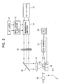
- Fig. 2 is a block diagram of a rewriting system for a three-dimensional optical memory element created in glass with ultrashort light pulses, showing an embodiment of the present invention.
- reference numeral 11 denotes an Ar + laser
- numeral 12 denotes a mode locked Ti:sapphire laser
- numeral 13 denotes an Nd:YLF laser
- numeral 14 denotes a regenerative amplifier
- numeral 15 denotes an ND filter
- numeral 16 denotes a mirror
- numeral 17 denotes a condensing lens
- numeral 18 denotes glass
- numeral 19 denotes an XYZ stage
- numeral 20 denotes a halogen lamp
- numeral 21 denotes a CCD camera
- numeral 22 denotes a computer.
- the Ti:sapphire laser is emitted onto the glass 18 set on the XYZ stage 19 through the condensing lens 17 to create bits (spots, voids, cavities).
- the stored bits can be rewritten as will be described later.
- the state of the bits can be imaged by light emitted from the halogen lamp 20 with the CCD camera 21.
- the Ti:sapphire laser (wavelength: 800 nm, power: 1 mW, pulse width: 130 fs, repetition frequency: 1 kHz) is used, with an exposure time of 1/125 s, using an electromagnetic shutter.
- the numerical aperture (NA) of the lens is 0.55, eight shots are taken, the strength during writing is 0.95 ⁇ J, the strength during transfer is 0.74 ⁇ J.
- the bits are created at a depth of 300 ⁇ m from the surface.
- the laser was emitted so as to be 0.1 ⁇ m shifted from a previously created bit 23, as shown in Fig. 3.
- the glass was a silica glass, in which the bit 23 could be shifted only when irradiated with the laser beam, with a focal light point 24 shifted in the opposite direction from the traveling direction of the laser beam, toward this side seen from the laser, being unable to be moved by a backward shift.
- Fig. 4 is a diagram showing a first transferring process for voids (bits) according to the present invention. After voids have been created once (refer to Fig. 4(a)), light is emitted such that a focal light point is shifted by 0.1 ⁇ m in the opposite direction to the direction of propagation of pulses (refer to Figs. 4(b) to 4(c)). In other words, the bits are rewritten under the condition shown in Fig. 3.
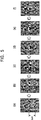
- Fig. 5 is a diagram showing a second transferring process for voids (bits) according to the present invention.
- bits voids
- a focal light point is shifted by 0.1 ⁇ m in the opposite direction to the direction of propagation of pulses to move the right void of the two to the left, thereby joining it with the other void (refer to Figs. 5(b) to 5(f)).
- the bits are rewritten under the condition shown in Fig. 2.
- the joined void becomes larger than the original ones.
- Fig. 6 is a diagram showing a third transferring process for voids (bits) according to the present invention. After voids have been created once (refer to Fig. 6(a)), they are shifted one by one to produce a dynamic memory (refer to Figs. 6(b) to 6(c)). The bits are rewritten under the condition shown in Fig. 3.
- the present invention has the following advantages:
- a rewritable three-dimensional memory element can be created. Also, application to the formation and correction of the contrast in index of refraction can be expected in the field of glass microfabrication.
- submicron-sized voids can be created at the focal light point. It was found that by condensing a femtosecond laser beam having a lower energy than that during manufacturing the voids slightly on this side of the submicron-sized voids seen from the laser, voids can be transferred.
- the submicron-sized voids are 5 ⁇ m shifted, so that the original voids or bits can be eliminated. The bits can also be combined.
- a method for rewriting data in a three-dimensional memory element created in glass with ultrashort light pulses is suitable for creating a rewritable three-dimensional memory element and for forming and correcting the contrast in index of refraction in the field of glass microfabrication. Also, it can be applied to the field of glass fabrication using a femtosecond laser, for example, to the field of correction of the contrast in index of refraction inside glass and glass microfabrication in manufacturing waveguides.
Landscapes
- Laser Beam Processing (AREA)
- Optical Integrated Circuits (AREA)
- Optical Modulation, Optical Deflection, Nonlinear Optics, Optical Demodulation, Optical Logic Elements (AREA)
- Read Only Memory (AREA)
Abstract
Description
Claims (5)
- A method for rewriting data in a three-dimensional optical memory element created in glass with ultrashort light pulses, characterized by comprising the steps of:(a) creating bits due to a photo-induced contrast in index of refractive inside the glass in three dimensions by the strength of a first ultrashort-pulse laser beam; and(b) irradiating the bits created in three dimensions with a second ultrashort-pulse laser beam having a lower energy than the strength of said first ultrashort-pulse laser beam, and when condensing the laser beam with an optical lens, condensing the laser beam at a point shifted from the bits to be moved by a predetermined distance in the opposite direction from the direction of propagation of the laser beam, thereby transferring the bit for rewriting.
- The method for rewriting data in a three-dimensional optical memory element created in glass with ultrashort light pulses according to Claim 1, characterized in that said creation of the bits is performed by differentiating the index of refraction in submicron-sized voids created by convergent irradiation of ultrashort laser-beam pulses of 1 ps or less from that in the vicinity of the bits.
- The method for rewriting data in a three-dimensional optical memory element created in glass with ultrashort light pulses according to Claim 1, characterized in that said transfer of the condensing point is performed a plurality of times so that the point is moved in stages.
- The method for rewriting data in a three-dimensional optical memory element created in glass with ultrashort light pulses according to Claim 1, characterized in that said glass is silica glass or silicate glass.
- The method for rewriting data in a three-dimensional optical memory element created in glass with ultrashort light pulses according to Claim 1, characterized in that said ultrashort-pulse laser beam is of 800 nm.
Applications Claiming Priority (3)
| Application Number | Priority Date | Filing Date | Title |
|---|---|---|---|
| JP2000145922 | 2000-05-18 | ||
| JP2000145922A JP3868713B2 (en) | 2000-05-18 | 2000-05-18 | Data rewriting method of three-dimensional optical memory device fabricated in glass by ultrashort light pulse |
| PCT/JP2001/004143 WO2001088925A1 (en) | 2000-05-18 | 2001-05-18 | Method for rewriting data in three-dimensional optical memory device fabricated in glass by ultra-short light pulse |
Publications (3)
| Publication Number | Publication Date |
|---|---|
| EP1306853A1 true EP1306853A1 (en) | 2003-05-02 |
| EP1306853A4 EP1306853A4 (en) | 2005-07-20 |
| EP1306853B1 EP1306853B1 (en) | 2006-08-30 |
Family
ID=18652358
Family Applications (1)
| Application Number | Title | Priority Date | Filing Date |
|---|---|---|---|
| EP01932127A Expired - Lifetime EP1306853B1 (en) | 2000-05-18 | 2001-05-18 | Method for rewriting data in three-dimensional optical memory device fabricated in glass by ultra-short light pulse |
Country Status (6)
| Country | Link |
|---|---|
| US (1) | US6897433B2 (en) |
| EP (1) | EP1306853B1 (en) |
| JP (1) | JP3868713B2 (en) |
| KR (1) | KR100535195B1 (en) |
| DE (1) | DE60122744T2 (en) |
| WO (1) | WO2001088925A1 (en) |
Families Citing this family (17)
| Publication number | Priority date | Publication date | Assignee | Title |
|---|---|---|---|---|
| JP4716663B2 (en) | 2004-03-19 | 2011-07-06 | 株式会社リコー | Laser processing apparatus, laser processing method, and structure manufactured by the processing apparatus or processing method |
| US7696625B2 (en) | 2004-11-30 | 2010-04-13 | Semiconductor Energy Laboratory Co., Ltd. | Semiconductor device and method for manufacturing the same |
| US7732349B2 (en) | 2004-11-30 | 2010-06-08 | Semiconductor Energy Laboratory Co., Ltd. | Manufacturing method of insulating film and semiconductor device |
| US7985677B2 (en) | 2004-11-30 | 2011-07-26 | Semiconductor Energy Laboratory Co., Ltd. | Method of manufacturing semiconductor device |
| US7517791B2 (en) | 2004-11-30 | 2009-04-14 | Semiconductor Energy Laboratory Co., Ltd. | Method for manufacturing semiconductor device |
| US7687326B2 (en) | 2004-12-17 | 2010-03-30 | Semiconductor Energy Laboratory Co., Ltd. | Semiconductor device and manufacturing method thereof |
| US7579224B2 (en) * | 2005-01-21 | 2009-08-25 | Semiconductor Energy Laboratory Co., Ltd. | Method for manufacturing a thin film semiconductor device |
| JP2006239718A (en) * | 2005-03-01 | 2006-09-14 | Kyoto Univ | Method and apparatus for producing nanopore periodic array |
| WO2016194032A1 (en) * | 2015-05-29 | 2016-12-08 | 株式会社日立製作所 | Optical device and optical device manufacturing method |
| US10248081B2 (en) | 2017-03-10 | 2019-04-02 | Microsoft Technology Licensing, Llc | Holographic phase and amplitude spatial light modulation |
| US10809529B2 (en) | 2017-06-15 | 2020-10-20 | Microsoft Technology Licensing, Llc | Optical device having multiplexed electrodes |
| US10181336B1 (en) | 2017-08-08 | 2019-01-15 | Microsoft Technology Licensing, Llc | Multi-beam optical system for fast writing of data on glass |
| US10236027B1 (en) | 2018-02-12 | 2019-03-19 | Microsoft Technology Licensing, Llc | Data storage using light of spatially modulated phase and polarization |
| RU2710389C1 (en) * | 2019-05-21 | 2019-12-26 | Российская Федерация, от имени которой выступает ФОНД ПЕРСПЕКТИВНЫХ ИССЛЕДОВАНИЙ | Information recording method in nanoporous quartzic glass |
| RU194317U1 (en) * | 2019-05-21 | 2019-12-05 | Российская Федерация, от имени которой выступает ФОНД ПЕРСПЕКТИВНЫХ ИССЛЕДОВАНИЙ | Glass data writer |
| RU2710387C1 (en) * | 2019-05-21 | 2019-12-26 | Российская Федерация, от имени которой выступает ФОНД ПЕРСПЕКТИВНЫХ ИССЛЕДОВАНИЙ | Information recording method in quartz glass |
| RU191298U1 (en) * | 2019-05-21 | 2019-08-01 | Российская Федерация, от имени которой выступает ФОНД ПЕРСПЕКТИВНЫХ ИССЛЕДОВАНИЙ | Glass Media Reader |
Family Cites Families (8)
| Publication number | Priority date | Publication date | Assignee | Title |
|---|---|---|---|---|
| JPS49106251A (en) | 1973-01-13 | 1974-10-08 | ||
| GB1362148A (en) * | 1973-01-18 | 1974-07-30 | Fajans J | Memory storage device and method of making the same |
| US4471470A (en) * | 1977-12-01 | 1984-09-11 | Formigraphic Engine Corporation | Method and media for accessing data in three dimensions |
| US5264876A (en) * | 1989-08-10 | 1993-11-23 | Canon Kabushiki Kaisha | Recording medium, method for preparing the same, recording and reproducing device, and recording, reproducing and erasing method by use of such recording medium |
| JP2961126B2 (en) * | 1995-02-13 | 1999-10-12 | セントラル硝子株式会社 | Recording medium comprising three-dimensional optical memory glass element and recording method thereof |
| AU711765B2 (en) * | 1995-11-28 | 1999-10-21 | Sri International | Two-step gated holographic recording in photorefractive materials using CW lasers |
| JP3657730B2 (en) | 1997-03-18 | 2005-06-08 | 株式会社東芝 | Information recording method for optical recording medium, information reproducing method for optical recording medium, recording apparatus and reproducing apparatus |
| JP3558855B2 (en) | 1998-02-19 | 2004-08-25 | 独立行政法人 科学技術振興機構 | Three-dimensional optical memory medium and method of manufacturing the same |
-
2000
- 2000-05-18 JP JP2000145922A patent/JP3868713B2/en not_active Expired - Fee Related
-
2001
- 2001-05-18 WO PCT/JP2001/004143 patent/WO2001088925A1/en not_active Ceased
- 2001-05-18 KR KR10-2002-7015568A patent/KR100535195B1/en not_active Expired - Fee Related
- 2001-05-18 DE DE60122744T patent/DE60122744T2/en not_active Expired - Fee Related
- 2001-05-18 US US10/276,695 patent/US6897433B2/en not_active Expired - Fee Related
- 2001-05-18 EP EP01932127A patent/EP1306853B1/en not_active Expired - Lifetime
Also Published As
| Publication number | Publication date |
|---|---|
| EP1306853A4 (en) | 2005-07-20 |
| KR100535195B1 (en) | 2005-12-08 |
| JP2001332092A (en) | 2001-11-30 |
| JP3868713B2 (en) | 2007-01-17 |
| US20030174552A1 (en) | 2003-09-18 |
| DE60122744T2 (en) | 2007-09-20 |
| US6897433B2 (en) | 2005-05-24 |
| EP1306853B1 (en) | 2006-08-30 |
| DE60122744D1 (en) | 2006-10-12 |
| WO2001088925A1 (en) | 2001-11-22 |
| KR20030005362A (en) | 2003-01-17 |
Similar Documents
| Publication | Publication Date | Title |
|---|---|---|
| EP1306853B1 (en) | Method for rewriting data in three-dimensional optical memory device fabricated in glass by ultra-short light pulse | |
| US5761111A (en) | Method and apparatus providing 2-D/3-D optical information storage and retrieval in transparent materials | |
| US7568365B2 (en) | Method and apparatus for micromachining bulk transparent materials using localized heating by nonlinearly absorbed laser radiation, and devices fabricated thereby | |
| US5951731A (en) | Laser processing method to a micro lens | |
| US12265245B2 (en) | Method of forming birefringent structures in an optical element | |
| JPH09311237A (en) | Optical waveguide and manufacturing method thereof | |
| EP1154413A3 (en) | Optical recording method and medium | |
| Watanabe et al. | Motion of bubble in solid by femtosecond laser pulses | |
| Huo et al. | The femtosecond laser fabrication of waveguide structures in transparent crystals | |
| Schaffer et al. | Micromachining using ultrashort pulses from a laser oscillator | |
| JP3468450B2 (en) | Method for selective reforming inside solid material and solid material having selectively reformed inside | |
| CA2031057C (en) | Fabrication of optical components utilizing a laser | |
| EP0919993A2 (en) | Method and apparatus for optically recording and reproducing information | |
| JP3967090B2 (en) | How to move voids inside transparent solids | |
| Miura et al. | Three-dimensional microscopic modifications in glasses by a femtosecond laser | |
| Wei et al. | F2-laser microfabrication of buried waveguide structures in transparent glasses | |
| Schaffer et al. | Micromachining and material change characterization using femtosecond laser oscillators | |
| JP2004530246A (en) | Non-erasable optical data storage device | |
| Coric et al. | Contrasts in writing photonic structures with ultrafast and ultraviolet lasers | |
| Glezer et al. | Ultrafast laser-induced microexplosions in transparent materials | |
| Glezer et al. | 3-D optical storage and engraving inside transparent materials | |
| Ma et al. | Precise processing of transparent material with femtosecond laser pulses | |
| TW202615912A (en) | Method and apparatus for generating a photonic element by simultaneously using two laser direct writing beams | |
| Chkalov et al. | Multilayer Volumetric Modification of Fused Silica by Femtosecond Laser Radiation | |
| Glezer et al. | 3-D optical data storage in transparent materials |
Legal Events
| Date | Code | Title | Description |
|---|---|---|---|
| PUAI | Public reference made under article 153(3) epc to a published international application that has entered the european phase |
Free format text: ORIGINAL CODE: 0009012 |
|
| 17P | Request for examination filed |
Effective date: 20021217 |
|
| AK | Designated contracting states |
Designated state(s): AT BE CH CY DE DK ES FI FR GB GR IE IT LI LU MC NL PT SE TR |
|
| AX | Request for extension of the european patent |
Extension state: AL LT LV MK RO SI |
|
| RBV | Designated contracting states (corrected) |
Designated state(s): AT BE CH CY DE FR GB LI NL |
|
| RAP1 | Party data changed (applicant data changed or rights of an application transferred) |
Owner name: JAPAN SCIENCE AND TECHNOLOGY AGENCY |
|
| RAP1 | Party data changed (applicant data changed or rights of an application transferred) |
Owner name: JAPAN SCIENCE AND TECHNOLOGY AGENCY |
|
| A4 | Supplementary search report drawn up and despatched |
Effective date: 20050607 |
|
| GRAP | Despatch of communication of intention to grant a patent |
Free format text: ORIGINAL CODE: EPIDOSNIGR1 |
|
| RBV | Designated contracting states (corrected) |
Designated state(s): DE FR GB NL |
|
| GRAS | Grant fee paid |
Free format text: ORIGINAL CODE: EPIDOSNIGR3 |
|
| GRAA | (expected) grant |
Free format text: ORIGINAL CODE: 0009210 |
|
| AK | Designated contracting states |
Kind code of ref document: B1 Designated state(s): DE FR GB NL |
|
| REG | Reference to a national code |
Ref country code: GB Ref legal event code: FG4D |
|
| REF | Corresponds to: |
Ref document number: 60122744 Country of ref document: DE Date of ref document: 20061012 Kind code of ref document: P |
|
| ET | Fr: translation filed | ||
| PGFP | Annual fee paid to national office [announced via postgrant information from national office to epo] |
Ref country code: NL Payment date: 20070503 Year of fee payment: 7 |
|
| PGFP | Annual fee paid to national office [announced via postgrant information from national office to epo] |
Ref country code: DE Payment date: 20070510 Year of fee payment: 7 |
|
| PLBE | No opposition filed within time limit |
Free format text: ORIGINAL CODE: 0009261 |
|
| STAA | Information on the status of an ep patent application or granted ep patent |
Free format text: STATUS: NO OPPOSITION FILED WITHIN TIME LIMIT |
|
| 26N | No opposition filed |
Effective date: 20070531 |
|
| PGFP | Annual fee paid to national office [announced via postgrant information from national office to epo] |
Ref country code: GB Payment date: 20070516 Year of fee payment: 7 |
|
| PGFP | Annual fee paid to national office [announced via postgrant information from national office to epo] |
Ref country code: FR Payment date: 20070510 Year of fee payment: 7 |
|
| GBPC | Gb: european patent ceased through non-payment of renewal fee |
Effective date: 20080518 |
|
| PG25 | Lapsed in a contracting state [announced via postgrant information from national office to epo] |
Ref country code: NL Free format text: LAPSE BECAUSE OF NON-PAYMENT OF DUE FEES Effective date: 20081201 |
|
| REG | Reference to a national code |
Ref country code: FR Ref legal event code: ST Effective date: 20090119 |
|
| PG25 | Lapsed in a contracting state [announced via postgrant information from national office to epo] |
Ref country code: FR Free format text: LAPSE BECAUSE OF NON-PAYMENT OF DUE FEES Effective date: 20080602 Ref country code: DE Free format text: LAPSE BECAUSE OF NON-PAYMENT OF DUE FEES Effective date: 20081202 |
|
| PG25 | Lapsed in a contracting state [announced via postgrant information from national office to epo] |
Ref country code: GB Free format text: LAPSE BECAUSE OF NON-PAYMENT OF DUE FEES Effective date: 20080518 |