EP1306741A2 - Data processing apparatus/device - Google Patents
Data processing apparatus/device Download PDFInfo
- Publication number
- EP1306741A2 EP1306741A2 EP02253111A EP02253111A EP1306741A2 EP 1306741 A2 EP1306741 A2 EP 1306741A2 EP 02253111 A EP02253111 A EP 02253111A EP 02253111 A EP02253111 A EP 02253111A EP 1306741 A2 EP1306741 A2 EP 1306741A2
- Authority
- EP
- European Patent Office
- Prior art keywords
- circuit
- supply voltage
- power supply
- produces
- data processing
- Prior art date
- Legal status (The legal status is an assumption and is not a legal conclusion. Google has not performed a legal analysis and makes no representation as to the accuracy of the status listed.)
- Granted
Links
Images





Classifications
-
- H—ELECTRICITY
- H04—ELECTRIC COMMUNICATION TECHNIQUE
- H04B—TRANSMISSION
- H04B1/00—Details of transmission systems, not covered by a single one of groups H04B3/00 - H04B13/00; Details of transmission systems not characterised by the medium used for transmission
- H04B1/06—Receivers
- H04B1/16—Circuits
- H04B1/1607—Supply circuits
-
- G—PHYSICS
- G06—COMPUTING OR CALCULATING; COUNTING
- G06F—ELECTRIC DIGITAL DATA PROCESSING
- G06F1/00—Details not covered by groups G06F3/00 - G06F13/00 and G06F21/00
- G06F1/26—Power supply means, e.g. regulation thereof
-
- G—PHYSICS
- G06—COMPUTING OR CALCULATING; COUNTING
- G06K—GRAPHICAL DATA READING; PRESENTATION OF DATA; RECORD CARRIERS; HANDLING RECORD CARRIERS
- G06K19/00—Record carriers for use with machines and with at least a part designed to carry digital markings
- G06K19/06—Record carriers for use with machines and with at least a part designed to carry digital markings characterised by the kind of the digital marking, e.g. shape, nature, code
- G06K19/067—Record carriers with conductive marks, printed circuits or semiconductor circuit elements, e.g. credit or identity cards also with resonating or responding marks without active components
- G06K19/07—Record carriers with conductive marks, printed circuits or semiconductor circuit elements, e.g. credit or identity cards also with resonating or responding marks without active components with integrated circuit chips
- G06K19/0701—Record carriers with conductive marks, printed circuits or semiconductor circuit elements, e.g. credit or identity cards also with resonating or responding marks without active components with integrated circuit chips at least one of the integrated circuit chips comprising an arrangement for power management
-
- G—PHYSICS
- G06—COMPUTING OR CALCULATING; COUNTING
- G06K—GRAPHICAL DATA READING; PRESENTATION OF DATA; RECORD CARRIERS; HANDLING RECORD CARRIERS
- G06K19/00—Record carriers for use with machines and with at least a part designed to carry digital markings
- G06K19/06—Record carriers for use with machines and with at least a part designed to carry digital markings characterised by the kind of the digital marking, e.g. shape, nature, code
- G06K19/067—Record carriers with conductive marks, printed circuits or semiconductor circuit elements, e.g. credit or identity cards also with resonating or responding marks without active components
- G06K19/07—Record carriers with conductive marks, printed circuits or semiconductor circuit elements, e.g. credit or identity cards also with resonating or responding marks without active components with integrated circuit chips
- G06K19/0723—Record carriers with conductive marks, printed circuits or semiconductor circuit elements, e.g. credit or identity cards also with resonating or responding marks without active components with integrated circuit chips the record carrier comprising an arrangement for non-contact communication, e.g. wireless communication circuits on transponder cards, non-contact smart cards or RFIDs
Definitions
- the present invention relates to a data processing apparatus and a data processing device.
- the present invention relates to a card-sized data processing device which executes prescribed tasks, extracting data and electric power from received electromagnetic waves such as a carrier wave that is modulated with an information signal.
- a data processing device is sometimes called a smart card.
- Card-sized data processing devices with contactless interfaces have become of interest in recent years, with growing expectations for their various applications, ranging from personal use (e.g., credit cards and commuter passes) to industrial use (e.g., electronic data tags for factory automation and warehouse management purposes). Such devices often provide processing functions to perform sophisticated tasks. To meet today's market needs, they have to have a microprocessor with a higher processing speed, inevitably resulting in increased power consumption.
- Some designers overcome this problem by optimizing the power supply system in a device, considering the operating voltage of each circuit block. More specifically, a lower supply voltage is provided to digital circuits that can operate at a relatively low voltage, while a higher supply voltage is fed to analog circuits that need a relatively high voltage to satisfy dynamic range requirements. By integrating two dedicated power supply circuits, the power consumption of card-sized data processing devices can be minimized.
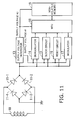
- FIG. 11 shows a typical structure of a known card-sized data processing device. As seen, the illustrated device is composed of the following elements: an antenna 10, four diodes 11-1 to 11-4, a supply voltage generator 13, a demodulator 14, a clock circuit 15, a reset circuit 16, a modulator 17, a microprocessor unit (MPU) 18, and a nonvolatile memory 19.
- an antenna 10 four diodes 11-1 to 11-4, a supply voltage generator 13, a demodulator 14, a clock circuit 15, a reset circuit 16, a modulator 17, a microprocessor unit (MPU) 18, and a nonvolatile memory 19.
- MPU microprocessor unit
- the antenna 10 emits and captures a radio wave to/from external card reader/writer equipment (not shown), which contains a carrier wave modulated with an information signal.
- the four diodes 11-1 to 11-4 form a bridge circuit, which full-wave rectifies the radio wave signal received by the antenna 10, thereby extracting the information signal and DC power.
- the supply voltage generator 13 From the DC power appearing at the junction point of the diodes 11-1 and 11-2, the supply voltage generator 13 produces a supply voltage #1 for analog circuits and a supply voltage #2 for digital circuits. More specifically, the supply voltage #1 is fed to the demodulator 14, clock circuit 15, reset circuit 16, and modulator 17, while the supply voltage #2 is fed to the MPU 18 and nonvolatile memory 19.
- FIG. 12 shows the detailed structure of the supply voltage generator 13.
- the supply voltage generator 13 is composed of a regulator 20, a first capacitor 21, a level converter 22, and a second capacitor 23.
- the regulator 20 With the electric power supplied through the diodes 11-1 and 11-2 (FIG. 11), the regulator 20 outputs a DC voltage with the level adjusted to the intended supply voltage #1.
- the first capacitor 21 reduces the output impedance of the regulator 20, besides eliminating ripple components contained in its output.
- the level converter 22 steps down the output of the regulator 20, from supply voltage #1 to supply voltage #2.
- the second capacitor 23 reduces the output impedance of the level converter 22, besides eliminating ripple components contained in its output.
- the demodulator 14 reproduces an information signal from the bridge output signal (i.e., the signal appearing at the junction point of the diodes 11-1 and 11-2) and sends the result to the MPU 18.
- the clock circuit 15 extracts a clock signal from the bridge output signal and sends it to the MPU 18.
- the reset circuit 16 produces a reset signal from the bridge output signal and sends it to the MPU 18.
- the modulator 17 modulates a carrier wave with an output data signal supplied from the MPU 18.
- the MPU 18 performs various computational operations according to firmware programs stored in the nonvolatile memory 19 and also to the incoming data signal supplied from the demodulator 14. The processing result is stored back into the nonvolatile memory 19 or supplied to the modulator 17 for transmission.
- the nonvolatile memory 19 is such a storage device that can retain the stored data even if the power supply is shut down. It stores programs and data that are necessary for the MPU 18 to execute its tasks.
- the demodulator 14, clock circuit 15, reset circuit 16, and modulator 17 operate at a supply voltage #1, while the MPU 18 and nonvolatile memory 19 operate at supply voltage #2 that is set to be lower than the supply voltage #1 so as to suppress their power consumption.
- the known device is configured in this way to improve its power requirements.
- the operating voltage of microprocessors has been going down with each passing year, and some processors available today can even operate at 1.8 V, for example.
- the supply voltage of nonvolatile memories stays at a relatively high level of about 3 V because such memory devices require a certain magnitude of energy to read or write data.
- This constraint of memory voltage leads to a problem with the known device shown in FIG. 11. That is, the circuit designer cannot reduce the supply voltage #2 further because the nonvolatile memory 19 does not allow it. In this sense, the nonvolatile memory 19 is a bottleneck in low-power design of such data processing devices.
- Another problem in the known circuit of FIG. 11 is that the MPU 18 and nonvolatile memory 19 are powered up at the same time.
- the nonvolatile memory 19 requires steadiness of its supply and control signal voltages for correct operation. Simultaneous activation of the MPU 18 may cause an unintended behavior of the nonvolatile memory 19 during the power-up.
- embodiments of the present invention may provide a data processing apparatus and card-sized data processing device which consume less power than known devices and operate reliably.
- a data processing apparatus which receives a radio wave modulated with an information signal and performs a prescribed task with data extracted from the received radio wave.
- This apparatus comprises a receiver and a first, second, and third power supply circuits.
- the receiver receives the radio wave and converts it into an electrical signal.
- the first power supply circuit produces a first supply voltage for use in an analog circuit.
- the second power supply circuit produces a second supply voltage that is different from the first supply voltage, for use in a memory circuit.
- the third power supply circuit produces a third supply voltage that is different from the first and second supply voltages, for use in a digital circuit.
- a second aspect of the present invention provides a card-sized data processing device which receives a radio wave modulated with an information signal and performs a prescribed task with data extracted from the received radio wave.
- This card-sized data processing device comprises a receiver and a first, second, and third power supply circuits.
- the receiver receives the radio wave and converts it into an electrical signal.
- the first power supply circuit produces a first supply voltage for use in an analog circuit.
- the second power supply circuit produces a second supply voltage that is different from the first supply voltage, for use in a memory circuit.
- the third power supply circuit produces a third supply voltage that is different from the first and second supply voltages, for use in a digital circuit.
- FIG. 1 is a conceptual view of a data processing apparatus according to the present invention.
- the proposed apparatus comprises: an antenna 30, a receiver 31, a first power supply circuit 32, an analog circuit 33, a second power supply circuit 34, a memory circuit 35, a third power supply circuit 36, and a digital circuit 37.
- the antenna 30 captures radio waves radiated from a remote transmitter (not shown).
- the receiver 31 converts the captured radio waves into an electronic signal.
- the first power supply circuit 32 produces a first supply voltage from the electrical signal that the receiver 31 outputs, and supplies it to the analog circuit 33.
- the second power supply circuit 34 produces a second supply voltage that is different from the first supply voltage and feeds it to the memory circuit 35.
- the third power supply circuit 36 produces a third supply voltage that is different from both the first and second supply voltages and feeds it to the digital circuit 37.
- the analog circuit 33 may be a modulator and demodulator, for example.
- the memory circuit 35 may be a nonvolatile memory, which stores data supplied from the digital circuit 37 and analog circuit 33.
- the digital circuit 37 and analog circuit 33 make access to data stored in the memory circuit 35 as necessary.
- the digital circuit 37 may be a microprocessor unit (MPU), for example, which performs various computational tasks according to firmware programs stored in the memory circuit 35.
- MPU microprocessor unit
- the apparatus of FIG. 1 operates as follows.
- the antenna 30 captures a radio wave transmitted from an external source (not shown) and feeds it to the receiver 31.
- the receiver 31 converts the captured radio wave into an electrical signal and then turns it to a DC signal, which is fed to the first power supply circuit 32.
- the first power supply circuit 32 produces a first supply voltage from this DC signal to energize the analog circuit 33.
- the second power supply circuit 34 then steps down the first supply voltage to produce a second supply voltage for the memory circuit 35.
- the third power supply circuit 36 steps down the second supply voltage to produce a third supply voltage for the digital circuit 37.
- the above circuit structure enables the first supply voltage, the highest among the three, to be provided to the analog circuit 33 that needs a relatively high voltage to ensure a sufficient dynamic range. It also provides the third supply voltage to the digital circuit 37 which can operate at a relatively lower voltage than the other two circuits do.
- the second supply voltage a middle level between the first and third voltages, is supplied to the memory circuit 35 whose operating voltage is higher than that of the digital circuit 37 but lower than that of the analog circuit 33. In this way, the present invention lowers the supply voltage of the digital circuit 37, which is always activated when the data processing apparatus is in use. As a result, the total power consumption of the apparatus is reduced.
- the memory circuit 35 is not the only load of the second power supply circuit 34. That is, the second power supply circuit 34 has to feed constantly a certain amount of power to the third power supply circuit 36 to keep the digital circuit 37 active. The presence of this constant load current ensures stable operation of the second power supply circuit 34.
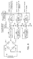
- FIG. 2 is a block diagram of a first embodiment of the present invention, which shows a card-sized data processing device comprising the following elements: an antenna 10, diodes 11-1 to 11-4, a supply voltage generator 50, a demodulator 14, a clock circuit 15, a reset circuit 16, a modulator 17, an MPU 18, and a nonvolatile memory 19.
- the antenna 10 emits or captures a radio wave to/from card reader/writer equipment (not shown), where the radio wave contains a carrier wave component that is modulated with, for example, amplitude shift keying (ASK) techniques.
- ASK amplitude shift keying
- diodes 11-1 to 11-4 form a bridge circuit, which full-wave rectifies the radio wave signal received by the antenna 10, thus isolating an information signal from the carrier, as well as extracting DC power therefrom.
- the supply voltage generator 50 produces three kinds of supply voltages #1 to #3. More specifically, the first supply voltage #1 is fed to the demodulator 14, clock circuit 15, reset circuit 16, and modulator 17. The second supply voltage #2 is fed to the nonvolatile memory 19, and the third supply voltage #3 is fed to the MPU 18.
- FIG. 3 shows the details of the supply voltage generator 50.
- the supply voltage generator 50 comprises the following elements: a regulator 60, a first capacitor 61, a first level converter 62, a second capacitor 63, and a second level converter 64, and a third capacitor 65.
- the regulator 60 From the DC power appearing at the junction point of the diodes 11-1 and 11-2, the regulator 60 outputs a DC voltage, adjusting its level to the intended supply voltage #1.
- the first capacitor 61 reduces the output impedance of the regulator 60, besides eliminating ripple components contained in its output.
- the first level converter 62 steps down the output of the regulator 60, from supply voltage #1 to supply voltage #2.
- the second capacitor 63 reduces the output impedance of the first level converter 62, besides eliminating ripple components contained in its output.
- the second level converter 64 steps down the output of the first level converter 62, from supply voltage #2 to supply voltage #3.
- the third capacitor 65 reduces the output impedance of the second level converter 64, besides eliminating ripple components contained in its output.
- FIG. 4 shows the details of the regulator 60.
- the regulator 60 comprises resistors 71, 72, and 74, a comparator 73, and an n-channel MOSFET 75. These components as a whole form a shunt regulator, assuming that the receiver 31 (FIG. 1) serves as a constant current source, or that there is a certain amount of output resistance at the source end.
- the first two resistors 71 and 72 serve as a voltage divider which provides a fraction of the output voltage to the non-inverting input of the comparator 73 as a feedback.
- the comparator 73 compares this divided voltage with the reference voltage Vref and supplies the result to the gate of the n-channel MOSFET 75. According to this signal, the n-channel MOSFET 75 varies its resistance to make a certain amount of current flow to the ground, so that the output voltage be maintained at the set level.
- the third resistor 74 is a current-limiting resistor that protects the n-channel MOSFET 75 from overcurrent. In this way, the circuit of FIG. 4 works as a shunt regulator to yield a stabilized output voltage.
- FIG. 5 shows the details of the first and second level converters 62 and 64.
- each level converter 62 and 64 comprises the following components: a comparator 80, a switch 81, and two resistors 82 and 83.
- the resistors 82 and 83 form a voltage divider which feeds a fraction of the output voltage back to the non-inverting input of the comparator 73 for comparison with a given reference voltage.
- the result of the comparison is used to control the switch 81.
- the switch 81 is actually a p-channel MOSFET 90 shown in FIG. 6, which controls the current flowing from input to output, according to its gate voltage given by the comparator 80. That is, the circuit of FIG. 5 operates as a series regulator to yield an output voltage that is determined by the reference voltage Vref.
- the demodulator 14 reproduces a data signal from the bridge output signal (i.e., the signal appearing at the junction point of the diodes 11-1 and 11-2) and sends the result to the MPU 18.
- the clock circuit 15 extracts a clock signal from the bridge output signal and sends it to the MPU 18.
- the reset circuit 16 produces a reset signal from the bridge output signal and sends it to the MPU 18.
- the modulator 17 modulates a carrier wave with an output data signal supplied from the MPU 18.
- the MPU 18 performs various computational operations according to the programs stored in the nonvolatile memory 19 and also to the incoming data signal supplied from the demodulator 14. The processing result is saved back into the nonvolatile memory 19 or supplied to the modulator 17 for transmission.
- the nonvolatile memory 19 is a storage device that can retain the stored data even if the power supply is shut down. It stores programs and data that are necessary for the MPU 18 to execute its tasks.
- the above-described first embodiment operates as follows.
- the card-sized data processing device is designed to interact with a reader/writer device (not shown), which transmits a carrier wave with a certain radio frequency, ASK-modulated with information and clock signals.
- the antenna 10 captures this radio wave when the card-sized data processing device is placed in the vicinity of the reader/writer device.
- the electrical signal developed at the antenna 10 is then full-wave rectified into a DC signal by a bridge rectifier circuit consisting of four diodes 11-1 to 11-4.
- the regulator 60 produces a DC voltage, adjusting its level to an intended voltage, or supply voltage #1.
- the supply voltage #1 is fed to analog circuits, and charges up ⁇ the first capacitor 61 located at the output of the regulator 60.
- the first level converter 62 steps down it to another intended voltage, or supply voltage #2.
- the supply voltage #2 is fed to the nonvolatile memory 19, and charges up the second capacitor 63 located at the output of the first level converter 62.
- the second level converter 64 steps down it to yet another intended voltage, or supply voltage #3.
- the supply voltage #3 is fed to the MPU 18, and charges up the third capacitor 65 located at the output of the second level converter 64.
- the supply voltage #1 activates analog circuits, which include a demodulator 14, a clock circuit 15, a reset circuit 16, and a modulator 17.
- the clock circuit 15 begins producing a clock signal from the bridge output signal for use in the MPU 18.
- the reset circuit 16 asserts the reset input of the MPU 18 for a while and then negates it to make the MPU 18 start up, at which moment the supply voltage #3 has risen to its intended level.
- the activated MPU 18 makes access to the nonvolatile memory 19 to fetch the executable programs stored therein. This enables the MPU 18 to interact with the external reader/writer, receiving incoming data from the demodulator 14 and sending outgoing data to the modulator 17.
- the first embodiment of the present invention is configured to have a first level converter 62 to provide the nonvolatile memory 19 with its optimal operating voltage (i.e., supply voltage #2).
- the proposed circuit structure makes it possible to lower the supply voltage #3 for the MPU 18 without affecting the operation of the nonvolatile memory 19 or any other components in the device. This is effective in reducing the power consumption of the device since the MPU 18 is always activated during the interaction with external reader/writer equipment.
- the first embodiment provides the nonvolatile memory 19 with a dedicated, optimal power supply, which is decoupled from that of the MPU 18. This configuration ensures reliable reading and writing of data from/to the nonvolatile memory 19.
- the first embodiment of the present invention employs a plurality of level converters for operating different groups of circuitry. This arrangement prevents the circuits in a device from interfering with each other through a common power supply, thus ensuring more reliable operation of the device.
- FIG. 7 is a block diagram of a card-sized data processing device according to a second embodiment of the present invention.
- the illustrated device shares some common functions and signals with the first embodiment discussed in FIG. 2.
- the following explanation will focus on its distinctive points, while affixing like reference numerals to like elements.
- the second embodiment differs from the first embodiment in that it has a supply voltage generator 55 that is different from the foregoing supply voltage generator 50, and also in that the clock circuit 15 and reset circuit 16 are provided with a dedicated power source, named "supply voltage #0.”
- the other circuit blocks operate just as in the first embodiment shown in FIG. 2.
- FIG. 8 gives the details of the supply voltage generator 55 shown in FIG. 7. This circuit shares some common elements with the circuit discussed in FIG. 3. The following explanation will not cover them, while affixing like reference numerals to like elements.
- the supply voltage generator 55 of FIG. 8 differs from that of FIG. 3 in that three switches 110 to 112 are placed at the outputs of the regulator 60, first level converter 62, and second level converter 64, respectively. Another difference is a power supply controller 113 that is employed to control those switches 110 to 112.
- the switches 110 to 112 are MOSFET switches illustrated in FIG. 6.
- the first switch 110 controls power supply to the demodulator 14 and modulator 17 by turning on and off the supply voltage #1 produced by the regulator 60, according to a control signal sent from the power supply controller 113.
- the second switch 111 controls power supply to the nonvolatile memory 19 by turning on and off the supply voltage #2 produced by the first level converter 62, according to another control signal sent from the power supply controller 113.
- the third switch 112 controls power supply to the MPU 18 by turning on and off the supply voltage #3 produced by the second level converter 64, according to yet another control signal sent from the power supply controller 113.
- the power supply controller 113 is constructed with a timer and other components. When a certain level of voltage is developed at the diode bridge output, the power supply controller 113 starts counting the time with its integral timer circuit. It activates the two switches 110 and 112 one by one when the timer reaches each predetermined value. Besides, the power supply controller 113 may control the second switch 111 in such a way that the nonvolatile memory 19 will be powered only when there is an active access request.
- the second embodiment operates as follows.
- the card-sized data processing device interacts with a reader/writer device, using a radiofrequency carrier wave that is ASK-modulated with information and clock signals.
- the antenna 10 captures this radio wave when the card-sized data processing device has reached the vicinity of the reader/writer device.
- the electrical signal developed at the antenna 10 is then full-wave rectified into a DC signal by a bridge rectifier circuit consisting of four diodes 11-1 to 11-4.
- the regulator 60 in the supply voltage generator 55 produces a DC voltage, adjusting its level to an intended voltage, i.e., supply voltage #0.
- FIG. 9 is a timing diagram showing how the voltages at nodes #1 to #3 and power supply voltages #0 to #3 vary with time in the second embodiment shown in FIG. 8.
- the voltage of node #1 i.e., output of regulator 60
- the clock circuit 15 and reset circuit 16 start supplying a clock signal and reset signal to the MPU 18.
- the reset circuit 16 resets signal to the MPU 18 for a predetermined period.
- the first level converter 62 With the active output of the regulator 60, the first level converter 62 begins its step-down operation. As a result, the voltage of node #2 starts to rise at time point t2 as shown in part (B) of FIG. 9, which enables the second level converter 64 to begin step-down operation, causing the voltage of node #3 to rise at time point t3 as shown in part (C) of FIG. 9.
- the power supply controller 113 turns on the first switch 110 at time point t4. Since this causes the supply voltage #1 to go up as shown in part (E) of FIG. 9, the demodulator 14 and modulator 17 become ready for operation. The power supply controller 113 then activates the third switch 112 at time point t5, making the supply voltage #3 rise as shown in part (G) of FIG. 9. The MPU 18 is powered up accordingly.
- the above-described sequence permits the clock circuit 15 and reset circuit 16 to receive the supply voltage #0 at time point t1. This is followed by the demodulator 14 and modulator 17, which receive the supply voltage #1 at time point t4, and then by the MPU 18, which receives the supply voltage #3 at time point t5. The MPU 18 is now able to interact with the external reader/writer, receiving incoming data from the demodulator 14 and sending outgoing data to the modulator 17.
- the power supply controller 113 detects this and thus turns on the second switch 111 at time point t6 as shown in part (F) of FIG. 9. As a result, the supply voltage #2 is fed to the nonvolatile memory 19, allowing the MPU 18 to write and read data to/from intended addresses. When this memory access from the MPU 18 is finished, the power supply controller 113 turns off the second switch 111 to stop feeding the supply voltage #2 to the nonvolatile memory 19.
- the second embodiment employs switches 110 to 112 to provide each supply voltage #1 to #3 at the right timing.
- This feature ensures reliable operation of the nonvolatile memory 19 because it stays disabled until the control signals from the MPU 18 become stable.
- the arrangement of the second embodiment contributes to total power reduction of the device, since it energizes the nonvolatile memory 19 only when necessary.
- This power control technique may be applied not only to the nonvolatile memory 19, but also to other circuit blocks if they are used only occasionally.
- the device may activate a circuit with a large power consumption or a circuit that needs powering up earlier than any other ones. While, as mentioned earlier, different circuits could interfere with each other when they were connected to a common power supply, the above control policy prevents that kind of interference from happening.
- This sequence is initiated when the device shown in FIG. 7 has reached the vicinity of a reader/writer device. More specifically, it proceeds according to the following steps:
- the second embodiment shown in FIG. 7 can be implemented in the process explained above.
- the present invention can include a number of variations. Take the first level converter 62, for example. While it is placed at the output of the regulator 60 in the foregoing two embodiments, the first level converter 62 may be connected directly to the junction point of the diodes 11-1 and 11-2. Likewise, it is possible to configure the second level converter 64 such that it will receive source power directly from that same junction point, or from the output of the regulator 60.
- the transmission medium for information and operating power it would be possible to use a medium other than radio waves, such as infrared rays.
- the present invention should not be limited to card-sized data processing devices. Needless to say, it is possible to apply the concept of the present invention to other types of data processing devices. It should also be noted that the most part of the circuit shown in FIG. 2 or FIG. 7 can be implemented in a semiconductor device or devices.
- a data processing apparatus receives a radio wave modulated with an information signal and performs a prescribed task with data extracted from the received radio wave.
- the apparatus comprises a radio wave receiver and three power supply circuits.
- the receiver receives the radio wave and converts it into an electrical signal, from which the first power supply circuit produces a first supply voltage for use in an analog circuit.
- the second power supply circuit produces a second supply voltage that is different from the first supply voltage, for use in a memory circuit, and a third power supply circuit produces a third supply voltage that is different from the other voltages, for use in a digital circuit.
- the above arrangement of the present invention permits different circuits to operate with different supply voltages optimized for their individual requirements, thereby reducing the total power consumption of the apparatus, as well as ensuring correct operation of each part of the apparatus.
- Such features of the present invention are considered particularly beneficial for card-sized data processing devices, which are required to operate with less power consumption.
Landscapes
- Engineering & Computer Science (AREA)
- Theoretical Computer Science (AREA)
- Computer Hardware Design (AREA)
- Microelectronics & Electronic Packaging (AREA)
- Physics & Mathematics (AREA)
- General Physics & Mathematics (AREA)
- Computer Networks & Wireless Communication (AREA)
- General Engineering & Computer Science (AREA)
- Signal Processing (AREA)
- Power Sources (AREA)
- Near-Field Transmission Systems (AREA)
Abstract
Description
Claims (9)
- A data processing apparatus which receives a radio wave modulated with an information signal and performs a prescribed task with data extracted from the received radio wave, comprising:a receiver (31) which receives the radio wave and converts the received radio wave into an electrical signal;a first power supply circuit (32) which produces a first supply voltage from the electrical signal provided from said receiver, for use in an analog circuit (33) ;a second power supply circuit (34) which produces a second supply voltage that is different from the first supply voltage, for use in a memory circuit (35); anda third power supply circuit (36) which produces a third supply voltage that is different from the first and second supply voltages, for use in a digital circuit (37).
- The data processing apparatus according to claim 1, wherein:said second power supply circuit (34) produces the second supply voltage by stepping down the first supply voltage; andsaid third power supply circuit (36) produces the third supply voltage by stepping down the second supply voltage.
- The data processing apparatus according to claim 1 or 2, further comprising:a switch circuit (81,111) inserted between the second power supply circuit and the memory circuit; anda control circuit (80,113) which turns on said switch circuit after the second supply voltage becomes stable.
- The data processing apparatus according to claim 1 or 2, further comprising:a switch circuit (81,111) inserted between the second power supply circuit and the memory circuit; anda control circuit (80,113) which turns on said switch circuit to feed power to the memory circuit only when there is an active access request to the memory circuit.
- A card-sized data processing device which receives a radio wave modulated with an information signal and performs a prescribed task with data extracted from the received radio wave, comprising:a receiver (31) which receives the radio wave and converts the received radio wave into an electrical signal;a first power supply circuit (32) which produces a first supply voltage from the electrical signal provided from said receiver, for use in an analog circuit (33) ;a second power supply circuit (34) which produces a second supply voltage that is different from the first supply voltage, for use in a memory circuit (35) ; anda third power supply circuit (36) which produces a third supply voltage that is different from the first and second supply voltages, for use in a digital circuit (37).
- The card-sized data processing device according to claim 5, wherein:said second power supply circuit (34) produces the second supply voltage by stepping down the first supply voltage; andsaid third power supply circuit (36) produces the third supply voltage by stepping down the second supply voltage.
- The card-sized data processing device according to claim 5 or 6, further comprising:a switch circuit inserted between the second power supply circuit and the memory circuit; anda control circuit which turns on said switch circuit after the second supply voltage becomes stable.
- The card-sized data processing device according to claim 5 or 6, further comprising:a switch circuit inserted between the second power supply circuit and the memory circuit; anda control circuit which turns on said switch circuit to feed power to the memory circuit only when there is access to the memory circuit.
- An electronic device comprising:a receiver (31) which receives electromagnetic waves and converts the received electromagnetic waves into an electrical signal;a first power supply circuit (32) which produces a first supply voltage from the electrical signal provided from said receiver, for use in a first circuit (33) ;a second power supply (34) circuit which produces a second supply voltage that is different from the first supply voltage, for use in a second circuit (35) ; anda third power supply circuit (36) which produces a third supply voltage that is different from the first and second supply voltages, for use in a third circuit (37).
Applications Claiming Priority (2)
| Application Number | Priority Date | Filing Date | Title |
|---|---|---|---|
| JP2001330644 | 2001-10-29 | ||
| JP2001330644A JP3923297B2 (en) | 2001-10-29 | 2001-10-29 | Information processing apparatus and card type information processing device |
Publications (3)
| Publication Number | Publication Date |
|---|---|
| EP1306741A2 true EP1306741A2 (en) | 2003-05-02 |
| EP1306741A3 EP1306741A3 (en) | 2004-05-12 |
| EP1306741B1 EP1306741B1 (en) | 2017-11-29 |
Family
ID=19146346
Family Applications (1)
| Application Number | Title | Priority Date | Filing Date |
|---|---|---|---|
| EP02253111.5A Expired - Lifetime EP1306741B1 (en) | 2001-10-29 | 2002-05-02 | Data processing apparatus/device |
Country Status (3)
| Country | Link |
|---|---|
| US (1) | US6970690B2 (en) |
| EP (1) | EP1306741B1 (en) |
| JP (1) | JP3923297B2 (en) |
Cited By (4)
| Publication number | Priority date | Publication date | Assignee | Title |
|---|---|---|---|---|
| WO2004013807A1 (en) * | 2002-07-30 | 2004-02-12 | Koninklijke Philips Electronics N.V. | Transponder with two supply voltages |
| US7738839B2 (en) | 2005-05-30 | 2010-06-15 | Semiconductor Energy Laboratory Co., Ltd | Semiconductor device and driving method thereof |
| US9123581B2 (en) | 2006-10-02 | 2015-09-01 | Semiconductor Energy Laboratory Co., Ltd. | Semiconductor device |
| KR20170007458A (en) * | 2014-05-28 | 2017-01-18 | 마이크론 테크놀로지, 인크 | Providing power availability information to memory |
Families Citing this family (16)
| Publication number | Priority date | Publication date | Assignee | Title |
|---|---|---|---|---|
| US6970694B2 (en) * | 2002-07-30 | 2005-11-29 | Interdigital Technology Corporation | Method and apparatus for mobile based access point name (APN) selection |
| JP3871667B2 (en) * | 2003-08-18 | 2007-01-24 | 松下電器産業株式会社 | Non-contact IC card |
| JP4363938B2 (en) * | 2003-09-26 | 2009-11-11 | シャープ株式会社 | Receiver |
| CN100438271C (en) * | 2004-01-30 | 2008-11-26 | 株式会社瑞萨科技 | Semiconductor integrated circuit device and non-contact IC card using it and portable information terminal |
| JP4169158B2 (en) * | 2004-12-24 | 2008-10-22 | インターナショナル・ビジネス・マシーンズ・コーポレーション | Wireless IC chip, position recognition system using the same, and security system |
| JP4842017B2 (en) * | 2005-05-30 | 2011-12-21 | 株式会社半導体エネルギー研究所 | Semiconductor device |
| US7639993B1 (en) * | 2005-08-26 | 2009-12-29 | Altera Corporation | Power supply circuitry for data signal transceivers on integrated circuits |
| KR100714729B1 (en) * | 2005-09-13 | 2007-05-07 | 엘지전자 주식회사 | Power generating device, portable terminal having same and control method thereof |
| JP2007122600A (en) | 2005-10-31 | 2007-05-17 | Fujitsu Ltd | Integrated circuit chip and RFID system |
| JP5038080B2 (en) * | 2006-10-02 | 2012-10-03 | 株式会社半導体エネルギー研究所 | Semiconductor device and electronic equipment |
| KR101134696B1 (en) * | 2007-01-12 | 2012-04-09 | 엘지전자 주식회사 | Electric power source management apparatus and method of mobile terminal |
| JP5183800B2 (en) * | 2009-04-15 | 2013-04-17 | ルネサスエレクトロニクス株式会社 | Semiconductor integrated circuit device and IC card mounting the same |
| KR101896921B1 (en) * | 2011-05-17 | 2018-09-12 | 삼성전자주식회사 | Wireless power receiver and method for controlling thereof |
| EP2891379B1 (en) * | 2012-08-30 | 2019-07-31 | University of Virginia Patent Foundation, D/B/A University of Virginia | Ultra low power sensing platform with multimodal radios |
| KR102593912B1 (en) | 2018-01-09 | 2023-10-26 | 삼성전자주식회사 | Mode-changeable power supply circuit and smart card including the same |
| US11086377B2 (en) * | 2018-04-29 | 2021-08-10 | Oracle International Corporation | Load line compensation in power monitoring |
Family Cites Families (19)
| Publication number | Priority date | Publication date | Assignee | Title |
|---|---|---|---|---|
| US4188585A (en) * | 1978-03-16 | 1980-02-12 | Cincinnati Electronics Corporation | Synchronized receiver power system |
| JPH0731303Y2 (en) * | 1986-02-18 | 1995-07-19 | 三洋電機株式会社 | Voltage generation circuit |
| JPH0460890A (en) * | 1990-06-29 | 1992-02-26 | Citizen Watch Co Ltd | Non-contact memory card |
| JPH07120403B2 (en) * | 1991-02-14 | 1995-12-20 | 高圧ガス工業株式会社 | IC card |
| JPH064857U (en) * | 1992-06-19 | 1994-01-21 | シチズン時計株式会社 | Data carrier |
| US5479172A (en) * | 1994-02-10 | 1995-12-26 | Racom Systems, Inc. | Power supply and power enable circuit for an RF/ID transponder |
| JPH0847251A (en) | 1994-07-29 | 1996-02-16 | Internatl Business Mach Corp <Ibm> | Switching regulator,information processor and its control method |
| JPH0855198A (en) * | 1994-08-15 | 1996-02-27 | Hitachi Ltd | Non-contact IC card |
| US5615004A (en) * | 1994-12-27 | 1997-03-25 | Hughes Electronics | Laser range finder power management system |
| US5574697A (en) * | 1995-08-15 | 1996-11-12 | Micron Technology, Inc. | Memory device with distributed voltage regulation system |
| JPH10302036A (en) * | 1997-04-25 | 1998-11-13 | Citizen Watch Co Ltd | Contactless type memory card |
| US6141283A (en) * | 1999-04-01 | 2000-10-31 | Intel Corporation | Method and apparatus for dynamically placing portions of a memory in a reduced power consumption state |
| JP2002544744A (en) * | 1999-05-17 | 2002-12-24 | ザ・グッドイヤー・タイヤ・アンド・ラバー・カンパニー | Programmable modulation index for transponder |
| US6659352B1 (en) | 1999-06-02 | 2003-12-09 | Matsushita Electric Industrial Co., Ltd. | Semiconductor integrated circuit, a contactless information medium having the semiconductor integrated circuit, and a method of driving the semiconductor integrated circuit |
| JP2001022452A (en) * | 1999-07-07 | 2001-01-26 | Mitsubishi Electric Corp | Power supply voltage step-down circuit |
| US6134130A (en) * | 1999-07-19 | 2000-10-17 | Motorola, Inc. | Power reception circuits for a device receiving an AC power signal |
| JP2001211640A (en) * | 2000-01-20 | 2001-08-03 | Hitachi Ltd | Electronic device, semiconductor integrated circuit, and information processing system |
| JP2001286080A (en) * | 2000-03-31 | 2001-10-12 | Seiko Epson Corp | Power receiving circuit, wireless communication device, and wireless communication system |
| WO2001075787A1 (en) | 2000-04-04 | 2001-10-11 | Koninklijke Philips Electronics N.V. | Data carrier having a chip including means for the controllable voltage supply to a further component of the data carrier |
-
2001
- 2001-10-29 JP JP2001330644A patent/JP3923297B2/en not_active Expired - Fee Related
-
2002
- 2002-04-29 US US10/133,322 patent/US6970690B2/en not_active Expired - Lifetime
- 2002-05-02 EP EP02253111.5A patent/EP1306741B1/en not_active Expired - Lifetime
Cited By (19)
| Publication number | Priority date | Publication date | Assignee | Title |
|---|---|---|---|---|
| WO2004013807A1 (en) * | 2002-07-30 | 2004-02-12 | Koninklijke Philips Electronics N.V. | Transponder with two supply voltages |
| US7289028B2 (en) | 2002-07-30 | 2007-10-30 | Nxp B.V. | Transponder with two supply voltages |
| US7738839B2 (en) | 2005-05-30 | 2010-06-15 | Semiconductor Energy Laboratory Co., Ltd | Semiconductor device and driving method thereof |
| US9123581B2 (en) | 2006-10-02 | 2015-09-01 | Semiconductor Energy Laboratory Co., Ltd. | Semiconductor device |
| KR20170007458A (en) * | 2014-05-28 | 2017-01-18 | 마이크론 테크놀로지, 인크 | Providing power availability information to memory |
| CN106415724A (en) * | 2014-05-28 | 2017-02-15 | 美光科技公司 | Providing power availability information to memory |
| EP3149733A4 (en) * | 2014-05-28 | 2018-01-03 | Micron Technology, INC. | Providing power availability information to memory |
| US9905275B2 (en) | 2014-05-28 | 2018-02-27 | Micron Technology, Inc. | Providing power availability information to memory |
| KR20180101634A (en) * | 2014-05-28 | 2018-09-12 | 마이크론 테크놀로지, 인크 | Providing power availability information to memory |
| KR101899231B1 (en) | 2014-05-28 | 2018-09-14 | 마이크론 테크놀로지, 인크 | Providing power availability information to memory |
| KR102001358B1 (en) | 2014-05-28 | 2019-07-17 | 마이크론 테크놀로지, 인크 | Providing power availability information to memory |
| US10424347B2 (en) | 2014-05-28 | 2019-09-24 | Micron Technology, Inc. | Providing power availability information to memory |
| CN106415724B (en) * | 2014-05-28 | 2020-02-18 | 美光科技公司 | Provide power availability information to memory |
| CN111292778A (en) * | 2014-05-28 | 2020-06-16 | 美光科技公司 | Provide power availability information to memory |
| US10796731B2 (en) | 2014-05-28 | 2020-10-06 | Micron Technology, Inc. | Providing power availability information to memory |
| US11250889B2 (en) | 2014-05-28 | 2022-02-15 | Micron Technology, Inc. | Providing power availability information to memory |
| US11749316B2 (en) | 2014-05-28 | 2023-09-05 | Micron Technology, Inc. | Providing power availability information to memory |
| CN111292778B (en) * | 2014-05-28 | 2023-12-12 | 美光科技公司 | Method for operating a memory device, memory device and electronic device |
| US12165730B2 (en) | 2014-05-28 | 2024-12-10 | Lodestar Licensing Group Llc | Providing power availability information to memory |
Also Published As
| Publication number | Publication date |
|---|---|
| JP2003132316A (en) | 2003-05-09 |
| EP1306741B1 (en) | 2017-11-29 |
| EP1306741A3 (en) | 2004-05-12 |
| JP3923297B2 (en) | 2007-05-30 |
| US20030083037A1 (en) | 2003-05-01 |
| US6970690B2 (en) | 2005-11-29 |
Similar Documents
| Publication | Publication Date | Title |
|---|---|---|
| US6970690B2 (en) | Data processing apparatus and card-sized data processing device | |
| AU725675B2 (en) | Data transaction device having contact and contactless modes of operation | |
| KR100471655B1 (en) | Data exchange system by contactless communication between terminal and remotely powered portable device | |
| US6079622A (en) | Non-contact information storage medium and data transmission method for the medium | |
| US8138893B2 (en) | Semiconductor integrated circuit device | |
| CN101015135A (en) | Radio frequency identification and communication device | |
| EP2340511B1 (en) | Contactless interface with supply voltage regulating circuit | |
| JP2000341171A (en) | Operation of very closely coupled electromagnetic transponder system | |
| US20070108301A1 (en) | Semiconductor device and IC card | |
| US7218204B2 (en) | Contactless IC card | |
| EP1560147B1 (en) | Power supply circuit that is stable against sudden load change | |
| KR102593912B1 (en) | Mode-changeable power supply circuit and smart card including the same | |
| CN109039387A (en) | The method of monitoring power level and corresponding non-contact communicating device | |
| KR20010029777A (en) | A semiconductor integrated circuit, a contactless information medium having the semiconductor integrated circuit, and a method of driving the semiconductor integrated circuit | |
| EP1527410B1 (en) | Transponder with a controllable power-on-reset circuit | |
| EP1527411B1 (en) | Transponder with two supply voltages | |
| KR100874983B1 (en) | Tag chip and its driving method | |
| US11050462B2 (en) | Combined RFID and power management architecture | |
| CN111753563A (en) | Passive RFID tag and RFID system | |
| US6792288B1 (en) | Analog interface for autonomous data exchange circuit | |
| US7571853B2 (en) | Device and method for supplying a data transfer unit with energy | |
| JP2005222278A (en) | Non-contact IC medium inlet, non-contact IC medium, and communication system using the same | |
| JPH10162108A (en) | Data storage | |
| JPH1153491A (en) | Data carrier system | |
| JP3697710B2 (en) | Data carrier and power supply used therefor |
Legal Events
| Date | Code | Title | Description |
|---|---|---|---|
| PUAI | Public reference made under article 153(3) epc to a published international application that has entered the european phase |
Free format text: ORIGINAL CODE: 0009012 |
|
| AK | Designated contracting states |
Designated state(s): AT BE CH CY DE DK ES FI FR GB GR IE IT LI LU MC NL PT SE TR |
|
| AX | Request for extension of the european patent |
Extension state: AL LT LV MK RO SI |
|
| PUAL | Search report despatched |
Free format text: ORIGINAL CODE: 0009013 |
|
| AK | Designated contracting states |
Kind code of ref document: A3 Designated state(s): AT BE CH CY DE DK ES FI FR GB GR IE IT LI LU MC NL PT SE TR |
|
| AX | Request for extension of the european patent |
Extension state: AL LT LV MK RO SI |
|
| 17P | Request for examination filed |
Effective date: 20041104 |
|
| AKX | Designation fees paid |
Designated state(s): DE FR GB |
|
| 17Q | First examination report despatched |
Effective date: 20061106 |
|
| RAP1 | Party data changed (applicant data changed or rights of an application transferred) |
Owner name: FUJITSU MICROELECTRONICS LIMITED |
|
| RAP1 | Party data changed (applicant data changed or rights of an application transferred) |
Owner name: FUJITSU SEMICONDUCTOR LIMITED |
|
| RAP1 | Party data changed (applicant data changed or rights of an application transferred) |
Owner name: FUJITSU SEMICONDUCTOR LIMITED |
|
| GRAP | Despatch of communication of intention to grant a patent |
Free format text: ORIGINAL CODE: EPIDOSNIGR1 |
|
| STAA | Information on the status of an ep patent application or granted ep patent |
Free format text: STATUS: GRANT OF PATENT IS INTENDED |
|
| INTG | Intention to grant announced |
Effective date: 20170623 |
|
| GRAS | Grant fee paid |
Free format text: ORIGINAL CODE: EPIDOSNIGR3 |
|
| GRAA | (expected) grant |
Free format text: ORIGINAL CODE: 0009210 |
|
| STAA | Information on the status of an ep patent application or granted ep patent |
Free format text: STATUS: THE PATENT HAS BEEN GRANTED |
|
| AK | Designated contracting states |
Kind code of ref document: B1 Designated state(s): DE FR GB |
|
| REG | Reference to a national code |
Ref country code: GB Ref legal event code: FG4D |
|
| REG | Reference to a national code |
Ref country code: DE Ref legal event code: R082 Ref document number: 60249187 Country of ref document: DE Representative=s name: HASELTINE LAKE KEMPNER LLP, DE Ref country code: DE Ref legal event code: R082 Ref document number: 60249187 Country of ref document: DE Representative=s name: HASELTINE LAKE LLP, DE |
|
| REG | Reference to a national code |
Ref country code: DE Ref legal event code: R096 Ref document number: 60249187 Country of ref document: DE |
|
| REG | Reference to a national code |
Ref country code: DE Ref legal event code: R097 Ref document number: 60249187 Country of ref document: DE |
|
| PLBE | No opposition filed within time limit |
Free format text: ORIGINAL CODE: 0009261 |
|
| STAA | Information on the status of an ep patent application or granted ep patent |
Free format text: STATUS: NO OPPOSITION FILED WITHIN TIME LIMIT |
|
| 26N | No opposition filed |
Effective date: 20180830 |
|
| REG | Reference to a national code |
Ref country code: DE Ref legal event code: R119 Ref document number: 60249187 Country of ref document: DE |
|
| GBPC | Gb: european patent ceased through non-payment of renewal fee |
Effective date: 20180502 |
|
| PG25 | Lapsed in a contracting state [announced via postgrant information from national office to epo] |
Ref country code: DE Free format text: LAPSE BECAUSE OF NON-PAYMENT OF DUE FEES Effective date: 20181201 Ref country code: GB Free format text: LAPSE BECAUSE OF NON-PAYMENT OF DUE FEES Effective date: 20180502 Ref country code: FR Free format text: LAPSE BECAUSE OF NON-PAYMENT OF DUE FEES Effective date: 20180531 |