EP1306726A1 - Development defect preventing process and material - Google Patents
Development defect preventing process and material Download PDFInfo
- Publication number
- EP1306726A1 EP1306726A1 EP01938668A EP01938668A EP1306726A1 EP 1306726 A1 EP1306726 A1 EP 1306726A1 EP 01938668 A EP01938668 A EP 01938668A EP 01938668 A EP01938668 A EP 01938668A EP 1306726 A1 EP1306726 A1 EP 1306726A1
- Authority
- EP
- European Patent Office
- Prior art keywords
- chemically amplified
- composition
- amplified photoresist
- development defects
- photoresist coating
- Prior art date
- Legal status (The legal status is an assumption and is not a legal conclusion. Google has not performed a legal analysis and makes no representation as to the accuracy of the status listed.)
- Ceased
Links
Classifications
-
- G—PHYSICS
- G03—PHOTOGRAPHY; CINEMATOGRAPHY; ANALOGOUS TECHNIQUES USING WAVES OTHER THAN OPTICAL WAVES; ELECTROGRAPHY; HOLOGRAPHY
- G03F—PHOTOMECHANICAL PRODUCTION OF TEXTURED OR PATTERNED SURFACES, e.g. FOR PRINTING, FOR PROCESSING OF SEMICONDUCTOR DEVICES; MATERIALS THEREFOR; ORIGINALS THEREFOR; APPARATUS SPECIALLY ADAPTED THEREFOR
- G03F7/00—Photomechanical, e.g. photolithographic, production of textured or patterned surfaces, e.g. printing surfaces; Materials therefor, e.g. comprising photoresists; Apparatus specially adapted therefor
- G03F7/26—Processing photosensitive materials; Apparatus therefor
- G03F7/38—Treatment before imagewise removal, e.g. prebaking
-
- G—PHYSICS
- G03—PHOTOGRAPHY; CINEMATOGRAPHY; ANALOGOUS TECHNIQUES USING WAVES OTHER THAN OPTICAL WAVES; ELECTROGRAPHY; HOLOGRAPHY
- G03F—PHOTOMECHANICAL PRODUCTION OF TEXTURED OR PATTERNED SURFACES, e.g. FOR PRINTING, FOR PROCESSING OF SEMICONDUCTOR DEVICES; MATERIALS THEREFOR; ORIGINALS THEREFOR; APPARATUS SPECIALLY ADAPTED THEREFOR
- G03F7/00—Photomechanical, e.g. photolithographic, production of textured or patterned surfaces, e.g. printing surfaces; Materials therefor, e.g. comprising photoresists; Apparatus specially adapted therefor
- G03F7/26—Processing photosensitive materials; Apparatus therefor
- G03F7/30—Imagewise removal using liquid means
- G03F7/32—Liquid compositions therefor, e.g. developers
- G03F7/322—Aqueous alkaline compositions
-
- G—PHYSICS
- G03—PHOTOGRAPHY; CINEMATOGRAPHY; ANALOGOUS TECHNIQUES USING WAVES OTHER THAN OPTICAL WAVES; ELECTROGRAPHY; HOLOGRAPHY
- G03F—PHOTOMECHANICAL PRODUCTION OF TEXTURED OR PATTERNED SURFACES, e.g. FOR PRINTING, FOR PROCESSING OF SEMICONDUCTOR DEVICES; MATERIALS THEREFOR; ORIGINALS THEREFOR; APPARATUS SPECIALLY ADAPTED THEREFOR
- G03F7/00—Photomechanical, e.g. photolithographic, production of textured or patterned surfaces, e.g. printing surfaces; Materials therefor, e.g. comprising photoresists; Apparatus specially adapted therefor
- G03F7/004—Photosensitive materials
- G03F7/09—Photosensitive materials characterised by structural details, e.g. supports, auxiliary layers
- G03F7/11—Photosensitive materials characterised by structural details, e.g. supports, auxiliary layers having cover layers or intermediate layers, e.g. subbing layers
-
- G—PHYSICS
- G03—PHOTOGRAPHY; CINEMATOGRAPHY; ANALOGOUS TECHNIQUES USING WAVES OTHER THAN OPTICAL WAVES; ELECTROGRAPHY; HOLOGRAPHY
- G03F—PHOTOMECHANICAL PRODUCTION OF TEXTURED OR PATTERNED SURFACES, e.g. FOR PRINTING, FOR PROCESSING OF SEMICONDUCTOR DEVICES; MATERIALS THEREFOR; ORIGINALS THEREFOR; APPARATUS SPECIALLY ADAPTED THEREFOR
- G03F7/00—Photomechanical, e.g. photolithographic, production of textured or patterned surfaces, e.g. printing surfaces; Materials therefor, e.g. comprising photoresists; Apparatus specially adapted therefor
- G03F7/16—Coating processes; Apparatus therefor
- G03F7/168—Finishing the coated layer, e.g. drying, baking, soaking
-
- G—PHYSICS
- G03—PHOTOGRAPHY; CINEMATOGRAPHY; ANALOGOUS TECHNIQUES USING WAVES OTHER THAN OPTICAL WAVES; ELECTROGRAPHY; HOLOGRAPHY
- G03F—PHOTOMECHANICAL PRODUCTION OF TEXTURED OR PATTERNED SURFACES, e.g. FOR PRINTING, FOR PROCESSING OF SEMICONDUCTOR DEVICES; MATERIALS THEREFOR; ORIGINALS THEREFOR; APPARATUS SPECIALLY ADAPTED THEREFOR
- G03F7/00—Photomechanical, e.g. photolithographic, production of textured or patterned surfaces, e.g. printing surfaces; Materials therefor, e.g. comprising photoresists; Apparatus specially adapted therefor
- G03F7/004—Photosensitive materials
- G03F7/0048—Photosensitive materials characterised by the solvents or agents facilitating spreading, e.g. tensio-active agents
-
- G—PHYSICS
- G03—PHOTOGRAPHY; CINEMATOGRAPHY; ANALOGOUS TECHNIQUES USING WAVES OTHER THAN OPTICAL WAVES; ELECTROGRAPHY; HOLOGRAPHY
- G03F—PHOTOMECHANICAL PRODUCTION OF TEXTURED OR PATTERNED SURFACES, e.g. FOR PRINTING, FOR PROCESSING OF SEMICONDUCTOR DEVICES; MATERIALS THEREFOR; ORIGINALS THEREFOR; APPARATUS SPECIALLY ADAPTED THEREFOR
- G03F7/00—Photomechanical, e.g. photolithographic, production of textured or patterned surfaces, e.g. printing surfaces; Materials therefor, e.g. comprising photoresists; Apparatus specially adapted therefor
- G03F7/004—Photosensitive materials
- G03F7/038—Macromolecular compounds which are rendered insoluble or differentially wettable
- G03F7/0382—Macromolecular compounds which are rendered insoluble or differentially wettable the macromolecular compound being present in a chemically amplified negative photoresist composition
-
- G—PHYSICS
- G03—PHOTOGRAPHY; CINEMATOGRAPHY; ANALOGOUS TECHNIQUES USING WAVES OTHER THAN OPTICAL WAVES; ELECTROGRAPHY; HOLOGRAPHY
- G03F—PHOTOMECHANICAL PRODUCTION OF TEXTURED OR PATTERNED SURFACES, e.g. FOR PRINTING, FOR PROCESSING OF SEMICONDUCTOR DEVICES; MATERIALS THEREFOR; ORIGINALS THEREFOR; APPARATUS SPECIALLY ADAPTED THEREFOR
- G03F7/00—Photomechanical, e.g. photolithographic, production of textured or patterned surfaces, e.g. printing surfaces; Materials therefor, e.g. comprising photoresists; Apparatus specially adapted therefor
- G03F7/004—Photosensitive materials
- G03F7/039—Macromolecular compounds which are photodegradable, e.g. positive electron resists
- G03F7/0392—Macromolecular compounds which are photodegradable, e.g. positive electron resists the macromolecular compound being present in a chemically amplified positive photoresist composition
-
- H—ELECTRICITY
- H10—SEMICONDUCTOR DEVICES; ELECTRIC SOLID-STATE DEVICES NOT OTHERWISE PROVIDED FOR
- H10P—GENERIC PROCESSES OR APPARATUS FOR THE MANUFACTURE OR TREATMENT OF DEVICES COVERED BY CLASS H10
- H10P76/00—Manufacture or treatment of masks on semiconductor bodies, e.g. by lithography or photolithography
- H10P76/20—Manufacture or treatment of masks on semiconductor bodies, e.g. by lithography or photolithography of masks comprising organic materials
- H10P76/204—Manufacture or treatment of masks on semiconductor bodies, e.g. by lithography or photolithography of masks comprising organic materials of organic photoresist masks
- H10P76/2041—Photolithographic processes
Definitions
- This invention relates to a process for forming a resist pattern having less development defects and good profiles using a chemically amplified photoresist, and to a composition for reducing development defects used in this process. More particularly, it relates to a process for forming a resist pattern which can form a resist pattern with good profiles by patternwise exposing a large-diameter substrate having formed thereon a chemically amplified photoresist coating, with preventing generation of development defects all over the large-diameter substrate, and to a composition for reducing development defects used in this process.
- lithographic technology has been employed in which a photoresist coating is formed on a substrate such as a silicon wafer and, after selectively irradiating this with actinic rays, is subjected to development processing to thereby form a resist pattern on the substrate.
- H7-181685 describe that an antireflective surface layer containing a fluorine-containing compound with a low refractive index is formed on a resist layer to thereby prevent detrimental influences of reflected light from the resist surface on formation of a resist pattern.
- To form an antireflective layer on a resist layer provides the advantage that, since degree of vibration amplitude of the thickness of a resist coating vs. sensitivity curve becomes smaller, fluctuation in sensitivity of resist becomes smaller even when thickness of the resist layer fluctuates, which leads to a decreased fluctuation in dimension of resist patterns formed.
- antireflective surface layer serves to decrease standing wave to be caused by interference between incident light and reflected light or between one reflected light and another reflected light.
- an underlying substrate is made plane to depress fluctuation in dimension due to fluctuation in thickness of the resist layer as described above, or a mask pattern is finely adjusted according to fluctuation in dimension of the resist.
- exposing apparatus there has been proposed a process of using a light source emitting radiation of a short wavelength, which is advantageous for forming a finer pattern, such as deep UV rays of KrF excimer laser (248 nm) or ArF excimer laser (193 nm) or, further, X rays or electron beams, and some of them have been coming into practice.
- a light source emitting radiation of a short wavelength which is advantageous for forming a finer pattern, such as deep UV rays of KrF excimer laser (248 nm) or ArF excimer laser (193 nm) or, further, X rays or electron beams, and some of them have been coming into practice.
- the chemically amplified photoresist is so susceptible to the influence of acidic substances, basic substances and moisture in the atmosphere that there results a change in dimension of a pattern--for example, a T-topped resist pattern results when a positive-working photoresist is used, or a round-topped resist pattern results when a negative-working photoresist is used--in case when the period between patternwise exposure to PEB (post exposure bake) is prolonged or due to intermixing with a resist.
- PEB post exposure bake
- defects upon developing a resist coating have become a problem.
- scumming in line-and-space type resists and opening failure in contact hole type resists There are illustrated scumming in line-and-space type resists and opening failure in contact hole type resists.
- Several causes may be considered for the opening failure of contact holes, but the most popular opening failure is that which is caused by residues after development.
- the causes for these defects there is illustrated insufficient dissolution of exposed portions into a developing solution due to insufficient contact between the developing solution containing water as a major component and the surface of a resist upon bringing the developing solution into contact with the resist surface, which leads to opening failure of portions which are designed to open.
- insolubles for the developing solution might re-deposit onto the surface of the resist upon rinsing with water after development.
- Japanese Unexamined Patent Publication No. H9-246166 proposes to treat the surface of a photoresist with plasma to thereby render the surface hydrophilic, thus improving wetting properties of the resist for a developing solution and decreasing development defects.
- This technique requires introduction of an additional apparatus for the plasma treatment and involves the problem of decrease in throughput.
- Japanese Examined Patent Publication No. H4-51020 describes to improve wetting properties of a positive-working resist for a developing solution by adding an acetylenealcohol type surfactant to the developing solution, thereby forming a pattern having no development defects. Although some effects can be obtained by this technique, the effects are at present still insufficient in ultra-fine working using the aforesaid chemically amplified photoresists. In addition, Japanese Unexamined Patent Publication No.
- S61-179435 describes to optionally conduct surface coating, which is effective for improving wetting properties for a developing solution, in addition to the method of adding a surfactant to the developing solution and the method of plasma-treating the surface of a resist coating, for preventing development defects resulting from lack of wetting properties for the developing solution.
- a paddle developing method has so far been popularly employed for developing a resist coating on the silicon wafer.
- a developing solution is dropped onto a resist coating formed on a substrate, and the substrate is spun to form a thin film of the developing solution all over the resist coating, thus development of the resist coating being conducted.
- developing conditions become different between the central portion of the wafer and the peripheral portion thereof.
- a process for forming a resist pattern has been desired earnestly which enables one to reduce development defects to be caused upon development including development defect to be caused in the periphery of a chemically amplified photoresist formed on a larger diameter substrate such as a silicon wafer, and which does not cause pattern failure such as T-top or round top after development, thus being adapted for forming a finer resist pattern.
- an object of the present invention is to provide a process for forming a resist pattern which can reduce development defects of a chemically amplified photoresist, formed on a large diameter substrate having a diameter of 8 inches or more, to be caused upon development and which does not cause deterioration of pattern profiles such as T-top or round top inconvenient for an etching step due to detrimental influences of a processing atmosphere and intermixing between the surface coating and the resist, and a composition for reducing development defects in this process.
- the inventors have found that the above-described object can be attained by increasing the amount of reduction in thickness of a resist after development in comparison with the case of not coating a composition for reducing development defects in a pattern-forming process wherein the composition for reducing development defects is applied on a chemically amplified photoresist coating formed on a substrate in order to render the surface of photoresist hydrophilic, followed by patternwise exposure and development to obtain a resist pattern, thus having achieved the present invention based on the finding.
- the present invention is a process for forming a resist pattern which includes: a step of forming a chemically amplified photoresist coating on a substrate having a diameter of 8 inches or more by application; a step of applying a composition for reducing development defects on the chemically amplified photoresist coating; a step of baking after at least either the step of forming the chemically amplified photoresist coating by application or the step of applying the composition for reducing development defects; a step of selectively exposing the chemically amplified photoresist coating; a step of post-exposure baking the chemically amplified photoresist coating; and a step of developing the chemically amplified photoresist coating, and which increases the amount of reduction in thickness of the chemically amplified photoresist coating after development by 10 ⁇ to 500 ⁇ in comparison with the case of not applying the composition for reducing development defects.
- the present invention is a composition for reducing development defects which is composed of an acidic composition containing a surfactant and which is to be used for the process for forming a resist pattern which includes: a step of forming a chemically amplified photoresist coating on a substrate having a diameter of 8 inches or more by application; a step of applying a composition for reducing development defects on the chemically amplified photoresist coating; a step of baking after at least either the step of forming the chemically amplified photoresist coating by application or the step of coating the composition for reducing development defects; a step of selectively exposing the chemically amplified photoresist coating; a step of post-exposure baking the chemically amplified photoresist coating; and a step of developing the chemically amplified photoresist coating, and which increases the amount of reduction in thickness of the chemically amplified photoresist coating after development by 10 ⁇ to 500 ⁇ in comparison with the case of not applying the composition for reducing development defects.
- the chemically amplified photoresist may be either of positive-working and negative-working types.
- the composition for reducing development defects to be used in the present invention preferably contains a surfactant and, when the chemically amplified photoresist is positive-working, the composition for reducing development defects is preferably acidic.
- PH of the composition is preferably 1.5 to 4.5, more preferably 1.7 to 3.5.
- the composition is preferably weakly acidic to alkaline.
- the surfactant to be used in the composition of the present invention for reducing development defects industrially utilized organic acids or the amine or ammonium salts thereof are preferably used.
- organic acid functional fluorocarbon compounds are preferred.
- the functional fluorocarbon compounds C 4 to C 15 perfluoroalkylcarboxylic acids and the ammonium salts, tetramethylammonium salts or C 1 to C 4 alkanolamine salts thereof; C 4 to C 10 perfluoroalkylsulfonic acids and the ammonium salts, tetramethylammonium salts or C 1 to C 4 alkanolamine salts thereof; fluorinated alkyl quaternary ammonium iodides; and perfluoroadipic acid and the quaternary ammonium salts thereof are preferred, with tetramethylammonium salts of C 7 to C 10 perfluoroalkylcarboxylic acids, C 4 to C 8 perfluoroalkylsulfonic acids
- surfactants are used as a 0.1 wt % - 25 wt %, more preferably 2 wt % - 4 wt % aqueous solution for the composition for reducing development defects.
- the ratio of the organic acid to the base is usually about 7:0 - 7:6 in molar ratio, preferably about 7:4 - 7:6, more preferably about 7:5.
- the molar ratio is usually about 7:0 - 1:6, preferably about 3:4 - 1:6, more preferably about 2:5.
- composition of the present invention for reducing development defects may further be added, if necessary, water-soluble resins and various additives within amounts not spoiling performance of the composition.
- water-soluble resin to be used in the composition for reducing development defects of the present invention there may be illustrated, for example, poly(vinyl alcohol), poly(acrylic acid), poly(vinylpyrrolidone), poly( ⁇ -trifluoromethylacrylic acid), poly(vinyl methyl ether-co-maleic anhydride), poly(ethylene glycol-co-propylene glycol), poly(N-vinylpyrrolidone-co-vinyl acetate), poly(N-vinylpyrrolidone-co-vinyl alcohol), poly(N-vinylpyrrolidone-co-acrylic acid), poly(N-vinylpyrrolidone-co-methyl acrylate), poly(N-vinylpyrrolidone-co-methacrylic acid), poly(N-vinylpyrrolidone-co-methyl methacrylate), poly(N-vinylpyrrolidone-co-maleic acid), poly(N-vinylpyrrolidone-co-
- surfactants to be added for improving coating properties such as nonionic surfactants, anionic surfactants and amphoteric surfactants.
- the nonionic surfactants are exemplified by polyoxyethylene alkyl ethers such as polyoxyethylene lauryl ether, polyoxyethylene oleyl ether and polyoxyethylene cetyl ether, polyoxyethylene fatty acid diesters, polyoxyfatty acid monoester, polyoxyethylene-polyoxypropylene block polymer, and acetylene glycol derivatives
- the anionic surfactants are exemplified by alkyldiphenyl ether disulfonic acids and the ammonium salts or organic amine salts thereof, alkyldiphenyl ether sulfonic acids and the ammonium salts or organic amine salts thereof, alkylbenzenesulfonic acids and the ammonium salts or organic amine salts thereof
- water to be used in the composition for reducing development defects of the present invention water from which organic impurities, metal ions, etc. have been removed by distillation, ion-exchange treatment, treatment through filter or various adsorption treatments are preferably used.
- a water-soluble organic solvent may be used together with water.
- the water-soluble organic solvent is not particularly limited as long as it can be soluble in water in a concentration of 0.1 wt % or more.
- the organic solvent include alcohols such as methyl alcohol, ethyl alcohol and isopropyl alcohol, ketones such as acetone and methyl ethyl ketone, esters such as methyl acetate and ethyl acetate, and polar solvents such as dimethylformamide, dimethylsulfoxide, methyl cellosolve, cellosolve, butyl cellosolve, cellosolve acetate, butylcarbitol and carbitol acetate.
- these specific examples are merely illustrated as examples of the organic solvents, and the organic solvents to be used in the present invention are not limited only to these solvents.
- optimization of reduction in thickness of resist coating in the present invention may also be attained by properly adjusting baking time or baking temperature of the resist and the composition for reducing development defects as well as optimization by the composition itself for reducing development defects.
- prebaking temperature for the resist there are generally two types in accordance with photoresist compositions to be used. That is, one type requires a high energy and generally requires to bake at a temperature of about 100 to 150 °C , and another type does not require so much energy in comparison with the former and requires to bake at a temperature of 100 °C or lower.
- prebaking temperature for the composition for reducing development defects is generally 60 to 100 °C which is high enough to remove the solvent.
- post-exposure baking of the resist is generally about 100 to 150 °C.
- formation of such T-tops can be in some cases avoided by such combination of baking temperatures for the resist and the composition for reducing development defects that resist-prebaking temperature is set at a lower level while prebaking temperature for the composition for reducing development defects at a level of 100 °C or higher.
- too much reduction in thickness of the resist coating disadvantageous in an etching step can be avoided by optionally delaminating or dissolving away the composition for reducing development defects after exposure.
- Thickness of the coating of the composition for reducing development defects in the present invention may be such that it provides enough chemical action to more reduce thickness of the resist coating in comparison with the case of not applying the composition for reducing development defects, and is preferably 80 to 10000 ⁇ , more preferably 330 to 990 ⁇ .
- Coating of the composition for reducing development defects can be conducted by any of known coating methods such as a spin coating method.
- the chemically amplified photoresist to be used in the present invention as a resist may be any of known positive-working and negative-working chemically amplified photoresists.
- the positive-working chemically amplified photoresist there are known a number of ones including that which is composed of a combination of a polymer wherein polyhydroxystyrene is protected with t-butoxycarbonyl group and a photo acid generator (see, H. Ito, and C. G. Willson: Polym. Eng. Sci., 23, 1012 (1983)).
- the negative-working chemically amplified photoresist there may be illustrated, for example, that which is composed of an alkali-soluble resin, a cross-linking agent of hexamethoxymelamine and a photo acid generator (for example, see, W. E. Feely, J. C. Imhof, C. M. Stein, T. A. Fisher and M. W. Legenza: Polym. Eng. Sci., 26, 1101(1986)).
- positive-working chemically amplified photoresists are preferred in the present invention. Thickness of the coating may be such that a resist pattern obtained after development can suitably exert its performance during etching in the etching step, and is generally about 0.3 to 1.0 ⁇ m.
- the pattern-forming method of the present invention can favorably be applied upon formation of a pattern on a substrate having a diameter of 8 inches or more.
- a silicon substrate is common, but may of course be those wherein a metal layer or a oxide or nitride layer such as silicon oxide, silicon nitride or silicon oxide nitride is formed on silicon.
- the substrate itself is not limited to silicon but may be any of substrate materials having so far been used for manufacturing IC such as LSI.
- any ones or any conditions having so far been employed for forming a resist pattern using a chemically amplified photoresist may be employed.
- an exposing light source to be used in the exposing step any of UV rays, deep UV rays, X rays and electron beams may be used.
- composition for reducing development defects had a pH of about 2.3.
- a positive-working chemically amplified photoresist containing a p-hydroxystyrene derivative was applied on an 8-inch silicon wafer in a varying thickness.
- the photoresist coating in a varying thickness of from about 0.67 ⁇ m to 0.81 ⁇ m after being prebaked.
- the prebaking was conducted at 90 °C for 90 seconds.
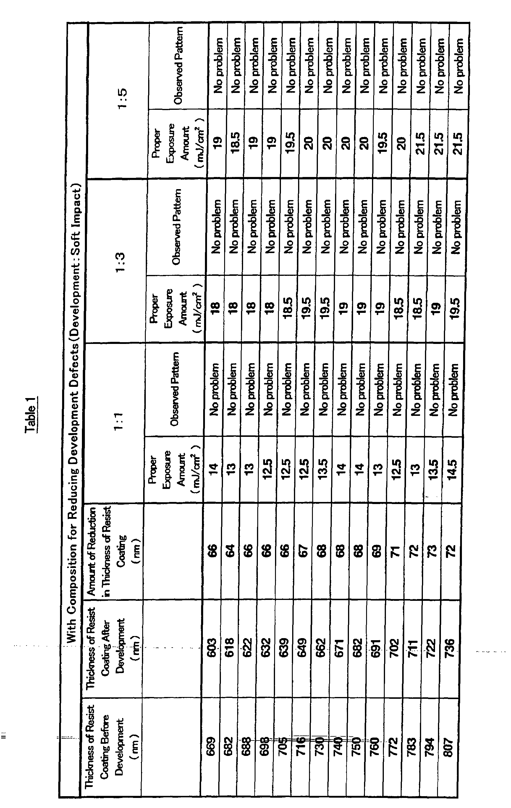
- the above-described composition for reducing development defects was applied on each of the wafers in a thickness of 440 ⁇ (without baking). Exposure was conducted using a halftone phase shift mask for contact hole having a mask size of 0.28 ⁇ m.
- FPA3000EX5 made by Canon Co., Ltd.
- Silicon wafers having coated thereon a positive-working chemically amplified photoresist with a varying thickness after baking were prepared in the same manner as in Example 1. Subsequent development, PEB and development were conducted in the same manner as in Example 1 except for not coating the composition for reducing development defects, and the wafers were observed under CD-SEM in the same manner as in Example 1. Results thus obtained are shown in Table 2. In comparison with Example 1, a number of development defects were observed. Additionally, "Opening failure was observed” means there existed some hole patterns not opened with a predetermined diameter.
- Silicon wafers having coated thereon a positive-working chemically amplified photoresist with a varying thickness after baking were prepared in the same manner as in Example 1. Subsequent development, PEB and development were conducted in the same manner as in Example 1 except for not coating the composition for reducing development defects and changing the developing method to a spraying method, and the wafers were observed under CD-SEM in the same manner as in Example 1. Results thus obtained are shown in Table 3. It is seen that, although development was conducted according to spraying method (paddle development as in Comparative Example 1) in which development defects are rather difficult to take place in comparison with the soft impact method due to more strict developing conditions employed in the spraying method, removal of development defects are still insufficient in comparison with Example 1 though better than in Comparative Example 1.
- the resist pattern-forming process of the present invention can form a resist pattern with good profiles which does not cause deterioration of pattern profile such as formation of T-top or round top and which, even when substrates having a diameter of 8 inches or more is used, does not cause development defects.
Landscapes
- Physics & Mathematics (AREA)
- General Physics & Mathematics (AREA)
- Engineering & Computer Science (AREA)
- Architecture (AREA)
- Structural Engineering (AREA)
- Photosensitive Polymer And Photoresist Processing (AREA)
- Materials For Photolithography (AREA)
- Exposure Of Semiconductors, Excluding Electron Or Ion Beam Exposure (AREA)
Abstract
Description


Claims (5)
- A process for forming a resist pattern which includes: a step of forming a chemically amplified photoresist coating on a substrate having a diameter of 8 inches or more by application; a step of applying a composition for reducing development defects on the chemically amplified photoresist coating; a step of baking after at least either the step of forming the chemically amplified photoresist coating by application or the step of applying the composition for reducing development defects; a step of selectively exposing the chemically amplified photoresist coating; a step of post-exposure baking the chemically amplified photoresist coating; and a step of developing the chemically amplified photoresist coating, and which increases the amount of reduction in thickness of the chemically amplified photoresist coating after development by 10 Å to 500 Å in comparison with the case of not applying the composition for reducing development defects.
- The method of forming resist patterns according to claim 1, wherein the composition for reducing development defects is an acidic composition containing a surfactant.
- The process for forming resist patterns according to claim 2, wherein the surfactant is at least one member selected from the group consisting of C4 to C15 perfluoroalkylcarboxylic acids and the ammonium salts, tetramethylammonium salts or C1 to C4 alkanolamine salts thereof, C4 to C10 perfluoroalkylsulfonic acids and the ammonium salts, tetramethylammonium salts or C1 to C4 alkanolamine salts thereof, fluorinated alkyl quaternary ammonium iodides, perfluoroadipic acid and the quaternary ammonium salts thereof.
- A composition for reducing development defects which is composed of an acidic composition containing a surfactant and which is to be used for the process for forming a resist pattern which includes: a step of forming a chemically amplified photoresist coating on a substrate having a diameter of 8 inches or more by application; a step of applying a composition for reducing development defects on the chemically amplified photoresist coating; a step of baking after at least either the step of forming the chemically amplified photoresist coating by application or the step of applying the composition for reducing development defects; a step of selectively exposing the chemically amplified photoresist coating; a step of post-exposure baking the chemically amplified photoresist coating; and a step of developing the chemically amplified photoresist coating, and which increases the amount of reduction in thickness of the chemically amplified photoresist coating after development by 10 Å to 500 Å in comparison with the case of not applying the composition for reducing development defects.
- The composition for reducing development defects according to claim 4, wherein the surfactant is at least one member selected from the group consisting of C4 to C15 perfluoroalkylcarboxylic acids and the ammonium salts, tetramethylammonium salts or C1 to C4 alkanolamine salts thereof, C4 to C10 perfluoroalkylsulfonic acids and the ammonium salts, tetramethylammonium salts or C1 to C4 alkanolamine salts thereof, fluorinated alkyl quaternary ammonium iodides, perfluoroadipic acid and the quaternary ammonium salts thereof.
Applications Claiming Priority (3)
| Application Number | Priority Date | Filing Date | Title |
|---|---|---|---|
| JP2000191364 | 2000-06-26 | ||
| JP2000191364A JP3320402B2 (en) | 2000-06-26 | 2000-06-26 | Development defect prevention process and materials |
| PCT/JP2001/005072 WO2002001299A1 (en) | 2000-06-26 | 2001-06-14 | Development defect preventing process and material |
Publications (2)
| Publication Number | Publication Date |
|---|---|
| EP1306726A1 true EP1306726A1 (en) | 2003-05-02 |
| EP1306726A4 EP1306726A4 (en) | 2007-04-04 |
Family
ID=18690674
Family Applications (1)
| Application Number | Title | Priority Date | Filing Date |
|---|---|---|---|
| EP01938668A Ceased EP1306726A4 (en) | 2000-06-26 | 2001-06-14 | METHOD AND MATERIAL FOR PREVENTING DEVELOPMENTAL ANOMALIES |
Country Status (8)
| Country | Link |
|---|---|
| US (1) | US7195863B2 (en) |
| EP (1) | EP1306726A4 (en) |
| JP (1) | JP3320402B2 (en) |
| KR (1) | KR100770551B1 (en) |
| CN (1) | CN1210626C (en) |
| MY (1) | MY131861A (en) |
| TW (1) | TWI221542B (en) |
| WO (1) | WO2002001299A1 (en) |
Cited By (2)
| Publication number | Priority date | Publication date | Assignee | Title |
|---|---|---|---|---|
| DE102006051766A1 (en) * | 2006-11-02 | 2008-05-08 | Qimonda Ag | Structured photo resist layer, on a substrate, uses selective illumination with separate acids and bakings before developing |
| US7799513B2 (en) | 2002-06-21 | 2010-09-21 | Az Electronic Materials Usa Corp. | Process for preventing development defect and composition for use in the same |
Families Citing this family (16)
| Publication number | Priority date | Publication date | Assignee | Title |
|---|---|---|---|---|
| US6955485B2 (en) * | 2002-03-01 | 2005-10-18 | Tokyo Electron Limited | Developing method and developing unit |
| US7799514B1 (en) * | 2004-10-01 | 2010-09-21 | Globalfoundries Inc | Surface treatment with an acidic composition to prevent substrate and environmental contamination |
| DE102005000858A1 (en) * | 2005-01-05 | 2006-07-20 | Merck Patent Gmbh | Use of trifluoromethoxy- or pentafluorosulfuranyl terminal groups as hydrophobic terminal groups in surface active compounds, which are useful as e.g. surfactants, hydrophobic agents, foam stabilizers and emulsifying agents |
| JP4968026B2 (en) * | 2007-11-30 | 2012-07-04 | Jsr株式会社 | Pattern formation method |
| JP5324290B2 (en) * | 2008-04-03 | 2013-10-23 | 東京応化工業株式会社 | Antireflection film forming material and resist pattern forming method using the same |
| JP5222111B2 (en) * | 2008-11-26 | 2013-06-26 | 東京応化工業株式会社 | Resist surface modification liquid and resist pattern forming method using the same |
| KR101585996B1 (en) | 2009-04-20 | 2016-01-18 | 삼성전자주식회사 | Photoresist composition, method of forming fine pattern using the same, and method of manufacturing semiconductor device |
| CN102486618A (en) * | 2010-12-02 | 2012-06-06 | 中芯国际集成电路制造(北京)有限公司 | Method for developing immersion photoresist without water-resistant surface coating |
| CN102169292B (en) * | 2011-03-17 | 2016-09-28 | 上海集成电路研发中心有限公司 | The coating process of photoresist |
| JP5965733B2 (en) * | 2012-06-12 | 2016-08-10 | 富士フイルム株式会社 | Pattern forming method and electronic device manufacturing method |
| RU2015128132A (en) | 2012-12-14 | 2017-01-18 | Басф Се | APPLICATION OF COMPOSITIONS CONTAINING SURFACE-ACTIVE SUBSTANCE AND MEANS OF GIVING HYDROPHOBICITY TO PROTECT THE RELIEF FROM DESTRUCTION WHEN PROCESSING RELIEF MATERIALS WITH LINEAR DIMENSIONS EQUAL TO 50 |
| TWI558850B (en) * | 2014-03-29 | 2016-11-21 | 精密聚合物股份有限公司 | Processing liquid for electronic parts and method of manufacturing electronic parts |
| TWI559082B (en) | 2014-07-07 | 2016-11-21 | 財團法人工業技術研究院 | Biomass material and method for manufacturing the same and print circuit board |
| CN107357140B (en) * | 2017-09-14 | 2021-05-04 | 江阴江化微电子材料股份有限公司 | Developing solution for positive photoresist and application thereof |
| CN112305860B (en) * | 2019-08-02 | 2024-12-13 | 东莞新科技术研究开发有限公司 | Exposure and development method for semiconductor |
| CN113564528B (en) * | 2021-06-18 | 2022-06-10 | 复旦大学 | A kind of light-controlled reversible hydrophobic element and preparation method thereof |
Family Cites Families (22)
| Publication number | Priority date | Publication date | Assignee | Title |
|---|---|---|---|---|
| JPS6232453A (en) * | 1985-08-06 | 1987-02-12 | Tokyo Ohka Kogyo Co Ltd | Developing solution for positive type photoresist |
| SG43691A1 (en) | 1991-06-28 | 1997-11-14 | Ibm | Top antireflective coating films |
| JPH05326389A (en) | 1992-05-20 | 1993-12-10 | Fujitsu Ltd | Method of forming resist pattern |
| JP3192505B2 (en) * | 1992-11-13 | 2001-07-30 | 東京応化工業株式会社 | Pattern forming method for semiconductor device manufacturing |
| JP2944857B2 (en) * | 1993-06-25 | 1999-09-06 | 日本電信電話株式会社 | Overcoat material |
| JP2803549B2 (en) * | 1993-12-21 | 1998-09-24 | 信越化学工業株式会社 | Light reflection preventing material and pattern forming method |
| US5631314A (en) * | 1994-04-27 | 1997-05-20 | Tokyo Ohka Kogyo Co., Ltd. | Liquid coating composition for use in forming photoresist coating films and photoresist material using said composition |
| JP2878150B2 (en) | 1994-04-27 | 1999-04-05 | 東京応化工業株式会社 | Coating solution for resist and resist material using the same |
| JPH07311467A (en) * | 1994-05-18 | 1995-11-28 | Hitachi Ltd | Water-soluble composition, pattern forming method using the same, and semiconductor device manufacturing method |
| JP2985688B2 (en) | 1994-09-21 | 1999-12-06 | 信越化学工業株式会社 | Water-soluble film material and pattern forming method |
| US5611850A (en) * | 1995-03-23 | 1997-03-18 | Mitsubishi Chemical Corporation | Composition for anti-reflective coating on resist |
| JP3336838B2 (en) * | 1995-08-22 | 2002-10-21 | 富士ゼロックス株式会社 | Electrostatic image developing toner, electrostatic image developer, and image forming method |
| JP3694703B2 (en) * | 1996-04-25 | 2005-09-14 | Azエレクトロニックマテリアルズ株式会社 | Anti-reflection coating composition |
| JPH09325500A (en) * | 1996-06-07 | 1997-12-16 | Mitsubishi Chem Corp | Surface antireflection coating composition and pattern forming method |
| JP3673399B2 (en) * | 1998-06-03 | 2005-07-20 | クラリアント インターナショナル リミテッド | Anti-reflection coating composition |
| JP3967466B2 (en) | 1998-06-19 | 2007-08-29 | 信越化学工業株式会社 | Anti-reflective coating material |
| JP2000275835A (en) * | 1999-03-25 | 2000-10-06 | Mitsubishi Chemicals Corp | Pattern formation method |
| JP2001023893A (en) * | 1999-07-12 | 2001-01-26 | Nec Corp | Method of forming photoresist pattern |
| JP3801398B2 (en) | 1999-11-01 | 2006-07-26 | 信越化学工業株式会社 | Antireflection film material and pattern forming method |
| JP2001215734A (en) * | 2000-02-04 | 2001-08-10 | Tokyo Ohka Kogyo Co Ltd | Method for reducing surface defects of resist pattern and treatment liquid for reducing surface defects used therein |
| JP3793920B2 (en) * | 2002-07-23 | 2006-07-05 | 株式会社リコー | Manufacturing method of electrophotographic toner, developer using the toner, developing method, transfer method, and process cartridge |
| US7358032B2 (en) * | 2002-11-08 | 2008-04-15 | Fujifilm Corporation | Planographic printing plate precursor |
-
2000
- 2000-06-26 JP JP2000191364A patent/JP3320402B2/en not_active Expired - Fee Related
-
2001
- 2001-05-22 TW TW090112204A patent/TWI221542B/en not_active IP Right Cessation
- 2001-06-13 MY MYPI20012748A patent/MY131861A/en unknown
- 2001-06-14 KR KR1020027017719A patent/KR100770551B1/en not_active Expired - Fee Related
- 2001-06-14 EP EP01938668A patent/EP1306726A4/en not_active Ceased
- 2001-06-14 CN CNB018116612A patent/CN1210626C/en not_active Expired - Fee Related
- 2001-06-14 WO PCT/JP2001/005072 patent/WO2002001299A1/en not_active Ceased
- 2001-06-14 US US10/311,787 patent/US7195863B2/en not_active Expired - Lifetime
Cited By (2)
| Publication number | Priority date | Publication date | Assignee | Title |
|---|---|---|---|---|
| US7799513B2 (en) | 2002-06-21 | 2010-09-21 | Az Electronic Materials Usa Corp. | Process for preventing development defect and composition for use in the same |
| DE102006051766A1 (en) * | 2006-11-02 | 2008-05-08 | Qimonda Ag | Structured photo resist layer, on a substrate, uses selective illumination with separate acids and bakings before developing |
Also Published As
| Publication number | Publication date |
|---|---|
| KR100770551B1 (en) | 2007-10-26 |
| EP1306726A4 (en) | 2007-04-04 |
| TWI221542B (en) | 2004-10-01 |
| WO2002001299A1 (en) | 2002-01-03 |
| KR20030076242A (en) | 2003-09-26 |
| CN1210626C (en) | 2005-07-13 |
| JP2002006514A (en) | 2002-01-09 |
| JP3320402B2 (en) | 2002-09-03 |
| US20030180667A1 (en) | 2003-09-25 |
| US7195863B2 (en) | 2007-03-27 |
| MY131861A (en) | 2007-09-28 |
| CN1439119A (en) | 2003-08-27 |
Similar Documents
| Publication | Publication Date | Title |
|---|---|---|
| US7195863B2 (en) | Development defect preventing process and material | |
| CN102736418B (en) | For the composition of coating on photo-resist pattern | |
| US7365115B2 (en) | Composition for antireflection coating and method for forming pattern | |
| US7018785B2 (en) | Method for forming pattern and treating agent for use therein | |
| US20040116312A1 (en) | Method for the removal of an imaging layer from a semiconductor substrate stack | |
| US20100324330A1 (en) | Process for Preventing Development Defect and Composition for Use in the Same | |
| KR20030043914A (en) | Process for manufacturing a microelectronic device | |
| US6692892B1 (en) | Composition for antireflection coating | |
| EP1061562A1 (en) | Method for forming resist pattern | |
| JP3779882B2 (en) | Development method, pattern formation method, photomask manufacturing method using these, and semiconductor device manufacturing method | |
| JP4957241B2 (en) | Resist pattern reducing material and fine resist pattern forming method | |
| KR20110013152A (en) | Mixed solution composition for improving roughness of positive photoresist pattern and method of using the same |
Legal Events
| Date | Code | Title | Description |
|---|---|---|---|
| PUAI | Public reference made under article 153(3) epc to a published international application that has entered the european phase |
Free format text: ORIGINAL CODE: 0009012 |
|
| 17P | Request for examination filed |
Effective date: 20030127 |
|
| AK | Designated contracting states |
Designated state(s): AT BE CH CY DE DK ES FI FR GB GR IE IT LI LU MC NL PT SE TR |
|
| RAP1 | Party data changed (applicant data changed or rights of an application transferred) |
Owner name: CLARIANT FINANCE (BVI) LIMITED |
|
| RAP1 | Party data changed (applicant data changed or rights of an application transferred) |
Owner name: AZ ELECTRONIC MATERIALS USA CORP. |
|
| A4 | Supplementary search report drawn up and despatched |
Effective date: 20070301 |
|
| RIC1 | Information provided on ipc code assigned before grant |
Ipc: G03F 7/32 20060101ALI20070223BHEP Ipc: G03F 7/11 20060101AFI20070223BHEP Ipc: G03F 7/38 20060101ALI20070223BHEP Ipc: G03F 7/16 20060101ALI20070223BHEP |
|
| 17Q | First examination report despatched |
Effective date: 20070509 |
|
| REG | Reference to a national code |
Ref country code: DE Ref legal event code: R003 |
|
| STAA | Information on the status of an ep patent application or granted ep patent |
Free format text: STATUS: THE APPLICATION HAS BEEN REFUSED |
|
| 18R | Application refused |
Effective date: 20110408 |