EP1304802A1 - Multiplexer circuit for converting parallel data into serial data at high speed and synchronized with a clock signal - Google Patents
Multiplexer circuit for converting parallel data into serial data at high speed and synchronized with a clock signal Download PDFInfo
- Publication number
- EP1304802A1 EP1304802A1 EP02252331A EP02252331A EP1304802A1 EP 1304802 A1 EP1304802 A1 EP 1304802A1 EP 02252331 A EP02252331 A EP 02252331A EP 02252331 A EP02252331 A EP 02252331A EP 1304802 A1 EP1304802 A1 EP 1304802A1
- Authority
- EP
- European Patent Office
- Prior art keywords
- multiplexer
- circuit
- transistors
- conductivity type
- power source
- Prior art date
- Legal status (The legal status is an assumption and is not a legal conclusion. Google has not performed a legal analysis and makes no representation as to the accuracy of the status listed.)
- Granted
Links
Images







Classifications
-
- H—ELECTRICITY
- H03—ELECTRONIC CIRCUITRY
- H03K—PULSE TECHNIQUE
- H03K17/00—Electronic switching or gating, i.e. not by contact-making and –breaking
- H03K17/51—Electronic switching or gating, i.e. not by contact-making and –breaking characterised by the components used
- H03K17/56—Electronic switching or gating, i.e. not by contact-making and –breaking characterised by the components used by the use, as active elements, of semiconductor devices
- H03K17/687—Electronic switching or gating, i.e. not by contact-making and –breaking characterised by the components used by the use, as active elements, of semiconductor devices the devices being field-effect transistors
- H03K17/693—Switching arrangements with several input- or output-terminals, e.g. multiplexers, distributors
-
- H—ELECTRICITY
- H03—ELECTRONIC CIRCUITRY
- H03M—CODING; DECODING; CODE CONVERSION IN GENERAL
- H03M9/00—Parallel/series conversion or vice versa
Definitions
- the present invention relates to a technique for carrying out a high-speed transmission of signals between LSIs or between devices formed by a plurality of LSIs. More particularly, the present invention relates to a multiplexer circuit that converts parallel data into serial data.
- the interface circuit that has the SerDes function it is necessary to convert relatively low-speed parallel data received from a logic circuit that carries out a data processing like a network switching, into high-speed serial data at Gbps speed, and output the converted data, for example.
- the data speed has become so fast, it has become necessary to improve time constants by preparing a separate current path, at a portion that has an upper limit in the operation frequency within the LSI circuit.
- a multiplexer circuit that converts parallel data into serial data carries out a data processing by using multi-phase clock signals, as described in "DIGITAL SYSTEMS ENGINEERING", Cambridge, 1998, by W, Dally et al. (for example, FIGURE 11-12 and FIGURE 11-25).
- DIGITAL SYSTEMS ENGINEERING Cambridge, 1998
- W, Dally et al. for example, FIGURE 11-12 and FIGURE 11-25.
- a multiplexer circuit having a plurality of multiplexer cells that receive parallel data, for converting the parallel data into serial data, and synchronized with a clock signal, wherein each of the multiplexer cells comprises a first load and a plurality of first conductivity type transistors that are connected in series between a first power source line and a second power source line; and a level-changing circuit that changes a connection node of adjacent first conductivity type transistors to a level of the first power source line.
- the multiplexer circuit may take out an output of each of the multiplexer cells from a connection node of the first load and the first conductivity type transistors that are connected in series.
- a plurality of the level-changing circuits may be provided at different positions of the connection node of the adjacent first conductivity type transistors.
- the level-changing circuit may be formed by at least one second conductivity type transistor that is connected to the first power source line.
- the first load may be formed by a second conductivity type transistor.
- the level-changing circuit may be formed by a second load that is connected to the first power source line and at least one first conductivity type transistor that is connected in series with the second load.
- the second load may be formed by a second conductivity type transistor.
- the first and second loads may be formed by second conductivity type transistors that are connected by cross coupling.
- the first and second loads may be formed by a parallel layout of second conductivity type transistors that are connected by cross coupling and second conductivity type transistors that are not connected by cross coupling.
- the first and second loads may be formed by second conductivity type transistors.
- the level-changing circuit may maintain the symmetry of the level-changing circuit in layout.
- the level-changing circuit may be formed by two second conductivity type transistors that are connected to the first power source line.
- Each of the multiplexer cells may be formed as a differential circuit that processes differential signals.
- the multiplexer circuit may further comprise a latching circuit that is provided at the outputs of the plurality of multiplexer cells.
- the first power source line may be a high-potential power source line
- the second power source line is a low-potential power source line
- the first conductivity type transistor may be an nMOS transistor
- the second conductivity type transistor may be a pMOS transistor.
- the multiplexer cells may be four multiplexer cells that are controlled based on four-phase clock signals.
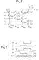
- Fig. 1 is a circuit diagram that shows one example of a conventional multiplexer circuit
- Fig. 2 is a timing diagram for explaining the operation of the multiplexer circuit shown in Fig. 1.
- Fig. 1 and Fig. 2 correspond to FIGURE 11-22 of the above-described literature.
- reference numbers 1001 to 1003, 1011 to 1013, 1021 to 1023, and 1031 to 1033 denote n-channel type MOS transistors (nMOS transistors).
- RT denotes a resistance
- ⁇ 0 to ⁇ 3 denote four-phase clock signals that have their phases mutually separated by 90 degrees respectively
- d0 to d3 denote parallel data.
- parallel data d0, d1, d2 and d3 are supplied to the gates of the transistors (input transistors) 1001, 1011, 1021 and 1031, respectively.
- Clock signals ( ⁇ 3 and ⁇ 0), ( ⁇ 0 and ⁇ 1), ( ⁇ 1 and ⁇ 2), and ( ⁇ 2 and ⁇ 3) are input to the transistors (1002 and 1003), (1012 and 1013), (1022 and 1023), and (1032 and 1033), respectively, that are connected in series with these input transistor. Data is taken in when each clock signal is at the high level "H".
- the data d0 is taken in when the clock signal ⁇ 3 and ⁇ 0 are both at the high level "H”.
- the data d1 is taken in when the clock signal ⁇ 0 and ⁇ 1 are both at the high level "H”.
- the data d2 is taken in when the clock signal ⁇ 1 and ⁇ 2 are both at the high level "H”.
- the data d3 is taken in when the clock signal ⁇ 2 and ⁇ 3 are both at the high level "H”.
- the parallel data d0 to d3 are converted into serial data in synchronism with the four-phase clock signals ( ⁇ 0 to ⁇ 3), and the serial data are transferred to an output OUT.
- Fig. 3 is a circuit diagram that shows another example of a conventional multiplexer circuit.
- Fig. 3 corresponds to FIGURE 11-25 of the above-described literature.
- reference numbers 1110 to 1117, 1120 to 1127, 1131 to 1133, and 1141 to 1143 denote nMOS transistors.
- Reference numbers 1134, 1135, 1144 and 1145 denotes loads.
- Clock signals ⁇ 0 to ⁇ 3 denote four-phase clock signals that have their phases mutually separated by 90 degrees respectively, and d0 to d3 denote parallel data.
- Clock signals / ⁇ 0 to / ⁇ 3 and data /d0 to /d3 denote inverted signals (signals of an opposite logic) of the clock signals ⁇ 0 to ⁇ 3 and the data d0 to d3, respectively. Therefore, the clock signal / ⁇ 0 is the same as the clock signal ⁇ 2, and the clock signal / ⁇ 1 is the same as the clock signal ⁇ 3, for example.
- a reference symbol Vc denotes a predetermined bias voltage that is applied to the gates of the transistors 1133 and 1143.
- Vr denotes a reference voltage that is applied to outputs OUT- and OUT+ via the loads 1144 and 1145 respectively.
- the multiplexer circuit shown in Fig. 3 uses differential (complementary) signals. Positive-logic parallel data d0, d1, d2, and d3 are taken in, when each pair of clock signals ( ⁇ 0 and / ⁇ 1), ( ⁇ 1 and / ⁇ 2), ( ⁇ 2 and / ⁇ 3), and ( ⁇ 3 and / ⁇ 0) that are supplied to the gates of corresponding transistors (1110 and 1120), (1112 and 1122), (1114 and 1124), and (1116 and 1126) have become at the high level "H". Each data is supplied to the gate of one transistor 1132 that constitutes a differential pair as serial data m.
- negative-logic parallel data /d0, /d1, /d2, and /d3 are taken in, when each pair of clock signals ( ⁇ 0 and / ⁇ 1), ( ⁇ 1 and / ⁇ 2), ( ⁇ 2 and / ⁇ 3), and ( ⁇ 3 and / ⁇ 0) that are supplied to the gates of corresponding transistors (1111 and 1121), (1113 and 1123), (1115 and 1125), and (1117 and 1127) have become at the high level "H".
- Each data is supplied to the gate of the other transistor 1131 that constitutes the differential pair as serial data /m.
- a differential amplifier that is constructed of the transistors 1131 to 1133 and the loads 1134 and 1135 acts as a pre-driver. Differential outputs p and /p of this pre-driver are supplied to differential inputs (the gates of the differential transistors 1141 and 1142) of an output-stage differential amplifier that is constructed of the transistors 1141 to 1143 and the loads 1144 and 1145. This output-stage differential amplifier outputs differential outputs OUT+ and OUT-.
- the conventional multiplexer circuits shown in Fig. 1 to Fig. 3 have the following problems to be solved.
- the parallel data d0 is at the high level "H”.
- the clock signals ⁇ 3 and ⁇ 0 are both at the high level “H”
- the transistors 1002 and 1003 are turned ON, and the potential of the output OUT is lowered to the low level “L” (Vss).
- the clock signal ⁇ 3 has fallen from the high level “H” to the low level “L”
- the transistor 1002 is turned OFF.
- the clock signal ⁇ 1 rises from the low level "L” to the high level "H”, thereby to turn ON the transistor 1013.
- the parallel data d0 and /d0 are supplied to the gates of the differential pair of transistors 1132 and 1131 of the pre-driver, via the transfer gates (transistors) (1110 and 1120) and (1111 and 1121) that are controlled based on the clock signals ⁇ 0 and / ⁇ 1, respectively.
- the transfer gates transistors (1110 and 1120) and (1111 and 1121) that are controlled based on the clock signals ⁇ 0 and / ⁇ 1, respectively.
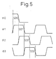
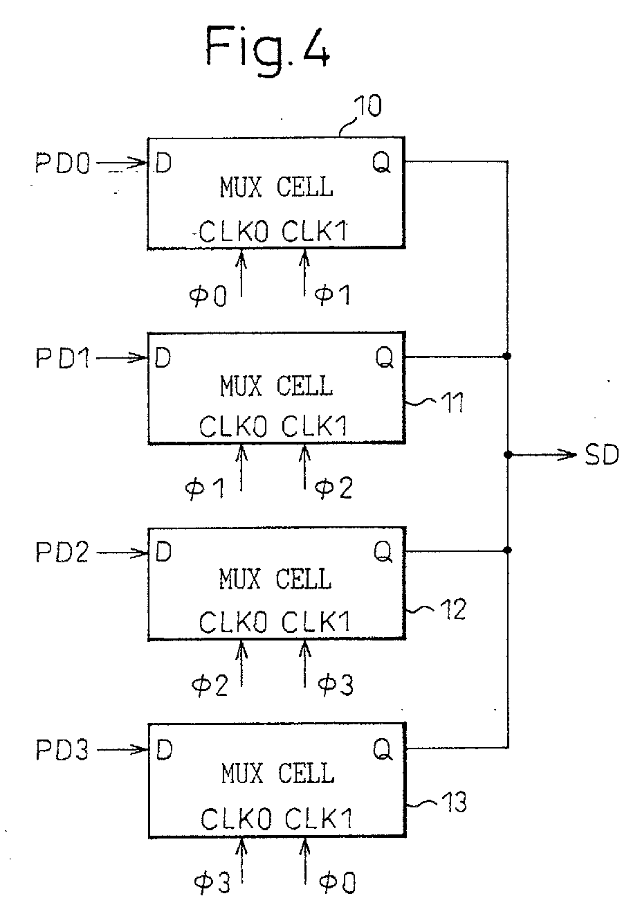
- Fig. 4 is a block diagram that shows one example of a total structure of a multiplexer circuit relating to the present invention
- Fig. 5 is a timing diagram for explaining the operation of the multiplexer circuit shown in Fig. 4.
- reference numbers 10 to 13 denote multiplexer cells
- PD0 to PD3 denoted parallel data
- SD denotes a serial data.
- the multiplexer circuit shown in Fig. 4 is an example of a multiplexer circuit of 4:1, it is needless to mention that the ratio is not limited to this in the present invention.
- the multiplexer circuit has four multiplexer cells 10 to 13.
- the multiplexer cells 10, 11, 12 and 13 are supplied with clock signals ( ⁇ 0 and ⁇ 1), ( ⁇ 1 and ⁇ 2), ( ⁇ 2 and ⁇ 3), and ( ⁇ 3 and ⁇ 0) respectively.
- the clock signals ⁇ 0 to ⁇ 3 are four-phase clock signals, and their phases are mutually deviated by 90 degrees respectively.
- the parallel data PD0 to PD3 are converted into serial data SD0 to SD3 in synchronism with the four-phase clock signals ⁇ 0 to ⁇ 3.
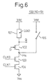
- Fig. 6 is a circuit diagram that shows a first embodiment of a multiplexer cell in the multiplexer circuit relating to the present invention.
- a multiplexer cell 100 (10 to 13) of the first embodiment is constructed of a load 101, nMOS transistors 102 to 104, and a pull-up switch (pull-up transistor) 105.
- the load 101 is provided between a high-potential power source line (Vdd) and an output node (output Q).
- Transistors 102 to 104 are connected in series between this output Q and a low-potential power source line (Vss).
- the transistor 102 receives an input data D (parallel data PD0 to PD3) at its gate, and drives the output Q.
- the transistors 103 and 104 carry out switching operation according to clock signals CLK0 and CLK1 that are supplied to their gates respectively.
- a connection node PN of the transistor 102 and the transistor 103 is connected to the high-potential power source line (Vdd).
- the driving transistor 102 determines the output data (Q) according to the input data D, when the transistors 103 and 104 for switching (for data confirmation) that are controlled based on the clock signals CLK0 and CLK1 respectively are turned ON.
- the input data D are the parallel data PD0 to PD3 for the multiplexer cells 10 to 13 respectively.
- the clock signals CLK0 to CLK1 are ( ⁇ 0 and ⁇ 1), ( ⁇ 1 and ⁇ 2), ( ⁇ 2 and ⁇ 3), and ( ⁇ 3 and ⁇ 0) for the multiplexer cells 10 to 13 respectively.
- the pull-up switch 105 that pulls up a voltage to the high-potential power source voltage Vdd is connected to the connection node PN of the driving transistor 102 and the data confirmation transistor 103.
- the pull-up switch 105 directly pulls up the node of the transistor 102 to which a data is input. Therefore, this structure is superior to that of the conventional example shown in Fig. 1 in the aspect of high-speed operation. Further, as the parallel input data D directly drive the gate of the nMOS transistor 102, it is possible to realize a high-speed operation, unlike the multiplexer circuit of the conventional example shown in Fig. 3.
- Fig. 7 is a circuit diagram that shows a second embodiment of a multiplexer cell relating to the present invention.
- a first pull-up switch 105 that pulls up a voltage to a high-potential power source voltage Vdd is provided for a connection node PN1 of a driving transistor 102 and a data confirmation transistor 103.
- a second pull-up switch 106 that pulls up a voltage to a high-potential power source voltage Vdd is provided for a connection node PN2 of the data confirmation transistor 103 and a data confirmation transistor 104.
- Fig. 8 is a circuit diagram that shows a third embodiment of a multiplexer cell relating to the present invention
- Fig. 9 is a timing diagram for explaining the operation of the multiplexer circuit shown in Fig. 8.
- the multiplexer cell of the third embodiment is constructed of pMOS transistors 111 and 112, and nMOS transistors 113 to 115.
- the transistors 111, 113 and 114 are connected in series between a high-potential power source line (Vdd) and a low-potential power source line (Vss).
- a clock signal CLK0 is supplied to the gates of the transistors 111 and 114.
- An input data D is supplied to the gate of the driving transistor 113.
- the pull-up transistor 112 has its source connected to the high-potential power source line (Vdd), and is supplied with the input data D at its gate. The drain of this pull-up transistor 112 is connected to a connection node of the transistors 111 and 113.
- the transistor 115 that is supplied with a clock signal CLK1 at its gate is inserted between an output Q and the connection node of the transistors 111 and 113.
- the transistor 113 is turned ON, the transistor 112 is turned OFF, and the clock signal ⁇ 0 (CLK1) changes from the low level “L” to the high level “H” (a period T0), based on the data PD0 at the high level “H”. Then, the transistor 114 is turned ON, the transistor 111 is turned OFF, and the node N1 is lowered to the low level “L” (the low-potential power source voltage Vss). Next, when the clock signal ⁇ 1 also changes from the low level “L” to the high level “H” (a period T1), the transistor 115 is turned ON, and the level of the node N1 becomes the output SD0.
- the transistor 113 is turned OFF, the transistor 112 is turned ON, the node N1 is increased to the high level “H” (maintains the high-potential power source voltage Vdd), and the clock signal ⁇ 0 changes from the low level “L” to the high level “H” (the period T0), based on the data PD0 at the low level “L”. Then, the transistor 114 is turned ON, and the transistor 111 is turned OFF. However, the node N1 maintains the high level "H”. Next, when the clock signal ⁇ 1 also changes from the low level "L” to the high level "H” (the period T1), the transistor 115 is turned ON, and the level of the node N1 becomes the output SD0.
- the pMOS transistors 111 and 112 are structured as small-sized transistors. When the multiplexer cell that operates next outputs the low level “L” in a status that the transistors 111 an d112 are in the ON status, for example, it is possible to instantaneously lower the level of the output node (Q) to the low level "L".
- a NAND-type transistor carries out a selection based on the clock signal CLK0 ( ⁇ 0), unlike the structure of the multiplexer circuit that has been explained with reference to Fig. 3.
- CLK0 clock signal
- Fig. 10 is a circuit diagram that shows a fourth embodiment of a multiplexer cell relating to the present invention.
- the multiplexer cell of the fourth embodiment is constructed of pMOS transistors 116 and 117, and nMOS transistors 113 to 115.
- the nMOS transistors 113 to 115 have a similar function to that of the nMOS transistors 113 to 115 in the third embodiment.
- the pMOS transistor 116 that is applied with a low-potential power source voltage Vss at its gate functions as a load element.
- the pMOS transistor 117 that is applied with a low-potential power source voltage Vss at its gate functions as a pull-up element.
- the transistor 114 that carries out a selection based on the clock signal CLK0 is disposed at the low-potential power source line (Vss) side of the data input transistor 113.
- Vss low-potential power source line
- Fig. 11 is a circuit diagram that shows a fifth embodiment of a multiplexer cell relating to the present invention. This multiplexer cell handles differential signals.
- the multiplexer cell of the fifth embodiment is constructed of pMOS transistors 121 and 122, and nMOS transistors 123 to 126.
- the pMOS transistors 121 and 122 that are applied with a low-potential power source voltage Vss at their gates function as load elements.
- the nMOS transistors 123 and 124 are a differential pair of transistors. Differential (complementary) input data D and DX (parallel data PD and XPD) are supplied to the gates of these transistors 123 and 124.
- the input data DX and the parallel data PDX show signals of the input data D and the parallel data PD of an inverted level respectively.
- the transistors 125 and 126 are provided between a differential amplifier section (the transistors 121 to 124) and a low-potential power source line (Vss).
- a clock CLK0 is supplied to the gate of the transistor 125
- a clock CLK1 is supplied to the gate of the transistor 126.
- the fifth embodiment corresponds to a structure of the first embodiment shown in Fig. 6 in which the load 101 is constructed of the transistor 121 (122), and the pull-up switch 105 is constructed of the transistors 122 and 124 (121 and 123).
- the fifth embodiment it is possible to realize a high-speed operation, by deleting the nMOS transistors (the transistors 1110, 1120, 1111, and 1121 in Fig. 3, for example) that are connected to the pull-up path of the output node. Further, according to the fifth embodiment, it is possible to realize a high-speed operation, by complementarily pulling up the node (PN) immediately below the nMOS transistor 123 that is supplied with an input data, with the transistors 122, 124, 121 and 123.
- PN node
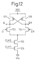
- Fig. 12 is a circuit diagram that shows a sixth embodiment of a multiplexer cell relating to the present invention.
- the load elements are structured with pMOS transistors 127 and 128 that are connected by cross coupling, in the multiplexer cell of the fifth embodiment. Based on this structure, it is possible to realize a high-speed operation while keeping a complementary relationship, by complementarily pulling up output nodes (Q and QX) that are driven by a differential pair of transistors 123 and 124.
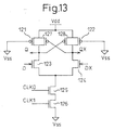
- Fig. 13 is a circuit diagram that shows a seventh embodiment of a multiplexer cell relating to the present invention.
- the multiplexer cell of the seventh embodiment includes both the transistors 121 and 122, and the transistors 127 and 128 of the fifth embodiment shown in Fig. 11 and the sixth embodiment shown in Fig. 12.
- the multiplexer cell of the sixth embodiment shown in Fig. 12 can compensate for differential (complementary) signals, even when there is a variation in the manufacturing of transistors, for example. However, the operation speed is lower, at this portion, than the operation speed of the multiplexer cell according to the fifth embodiment shown in Fig. 11.
- the multiplexer cell of the seventh embodiment has the advantages of both the fifth embodiment and the sixth embodiment.
- the pMOS loads 121 and 122 pull up the output nodes (Q and QX) that are driven by the pair of differential transistors 123 and 124.
- the cross-coupled loads 127 and 128 complementarily pull up these output nodes (Q and QX).
- the gates of the transistors 125 and 126, that are connected by cross coupling are connected to the drains of the two transistors 122 and 126, and 121 and 125, that are connected in parallel respectively, it is possible to reduce the drain load. This contributes to the high-speed operation.
- Fig. 14 is a circuit diagram that shows an eighth embodiment of a multiplexer cell relating to the present invention.
- the multiplexer cell of the eighth embodiment has pMOS transistors 131 and 132 that pull up a node (PN) immediately below the differential pair of transistors 123 and 124, in the multiplexer cell of the fifth embodiment.
- PN node
- a clock signal CLK0 that is supplied to the gate of an nMOS transistor 125 is supplied to the gates of the transistors 131 and 132 respectively.
- the transistors 131 and 132 are ON to pull up the node PN.
- the two pull-up transistors 131 and 132 are provided, in this case, in order to maintain symmetry of the circuit on the layout. Therefore, when it is possible to dispose a pull-up transistor at a center portion of a differential amplifier section (the transistors 121 to 124) on the layout, this pull-up transistor can be constituted by one transistor.
- the transistors 131 and 132 are ON to pull up the node PN, during a period while the transistor 125 is OFF. With this arrangement, it becomes possible to shorten a transition time of the node PN to an initial status. As a result, it becomes possible to realize a high-speed operation.
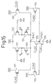
- Fig. 15 is a circuit diagram that shows a ninth embodiment of a multiplexer cell relating to the present invention.
- the multiplexer cell of the ninth embodiment has further pMOS transistors 133 and 134 that pull up a connection node (PN2) of the transistors 125 and 126, in the multiplexer cell of the eighth embodiment.
- pMOS transistors 131 and 132 pull up a node (PN1) immediately below differential pair of transistors 123 and 124, in a similar manner to that of the eighth embodiment.
- a clock signal CLK0 that is the same as that supplied to the gate of the transistor 125 is supplied to the gates of these transistors 131 to 134 respectively.
- the multiplexer cell of the ninth embodiment there are two pull-up positions (a plurality of positions) in a similar manner to that of the multiplexer cell of the second embodiment shown in Fig. 7. Therefore, it becomes possible to shorten a transition time of each node (PN1 and PN2) to an initial status. As a result, it becomes possible to realize a higher-speed operation.
- Fig. 16 is a circuit diagram that shows a tenth embodiment of a multiplexer cell relating to the present invention.
- the load elements (the pMOS transistors 121 and 122) of the differential amplifier section are structured with pMOS transistors 127 and 128 that are connected by cross coupling, in the multiplexer cell of the eighth embodiment.
- the load elements (the pMOS transistors 121 and 122) of the differential amplifier section are structured with pMOS transistors 127 and 128 that are connected by cross coupling, in the multiplexer cell of the eighth embodiment.
- Fig. 17 is a circuit diagram that shows an eleventh embodiment of a multiplexer cell relating to the present invention.
- the multiplexer cell of the eleventh embodiment is further provided with pMOS transistors 133 and 134 that pull up a connection node (PN2) of the transistors 125 and 126, in the multiplexer cell of the tenth embodiment shown in Fig. 16.
- PN2 connection node
- pMOS transistors 131 and 132 pull up a node (PN1) immediately below differential pair of transistors 123 and 124, in a similar manner to that of the tenth embodiment.
- a clock signal CLK0 that is the same as that supplied to the gate of the transistor 125 is supplied to the gates of these transistors 131 to 134 respectively.
- the multiplexer cell of the eleventh embodiment there are two pull-up positions (a plurality of positions) as in the multiplexer cell of the second embodiment shown in Fig. 7 and the ninth embodiment shown in Fig. 15. Therefore, it becomes possible to shorten a transition time of each node (PN1 and PN2) to an initial status. As a result, it becomes possible to realize a higher-speed operation.
- Fig. 18 is a circuit diagram that shows a twelfth embodiment of a multiplexer cell relating to the present invention.
- the multiplexer cell of the twelfth embodiment includes both the transistors 121 and 122, and the transistors 127 and 128 of the eighth embodiment shown in Fig. 14 and the tenth embodiment shown in Fig. 16.
- a differential amplifier section in the multiplexer cell of the eleventh embodiment is similar to that of the seventh embodiment explained with reference to Fig. 13.
- the pMOS loads 121 and 122 pull up the output nodes (Q and QX) that are driven by the pair of differential transistors 123 and 124.
- the cross-coupled loads 127 and 128 complementarily pull up these output nodes (Q and QX).
- the gates of the transistors 125 and 126 that are connected by cross coupling are connected to the drains of the two transistors 122 and 126, and 121 and 125, that are connected in parallel respectively, it is possible to reduce the drain load. This contributes to the high-speed operation.
- the transistors 131 and 132 are ON to pull up the node PN, during a period while the transistor 125 is OFF. With this arrangement, it becomes possible to shorten a transition time of the node PN to an initial status. As a result, it becomes possible to realize a high-speed operation, in a similar manner to that of the eighth embodiment and the tenth embodiment respectively.
- Fig. 19 is a circuit diagram that shows a thirteenth embodiment of a multiplexer cell relating to the present invention.
- pMOS transistors 133 and 134 that pull up a connection node (PN2) of the transistors 125 and 126, in the multiplexer cell of the twelfth embodiment shown in Fig. 18.
- PN2 connection node
- pMOS transistors 131 and 132 pull up a node (PN1) immediately below differential pair of transistors 123 and 124, in a similar manner to that of the tenth embodiment.
- a clock signal CLK0 that is the same as that supplied to the gate of the transistor 125 is supplied to the gates of these transistors 131 to 134 respectively.
- the multiplexer cell of the thirteenth embodiment there are two pull-up positions (a plurality of positions). This is similar to the multiplexer cell of the second embodiment shown in Fig. 7, the ninth embodiment shown in Fig. 15, and the eleventh embodiment shown in Fig. 17, respectively. Therefore, it becomes possible to shorten a transition time of each node (PN1 and PN2) to an initial status. As a result, it becomes possible to realize a higher-speed operation.
- Fig. 20 is a block diagram that shows another example of a total structure of a multiplexer circuit relating to the present invention.
- the multiplexers 10 to 13 in the multiplexer circuit shown in Fig. 4 are structured to be able to handle differential (complementary) signals (parallel input data PD0, PD0X to PD3, and PD3X, and serial output data SD and SDX). Further, a flip-flop (latch) that is constructed of two NAND gates 21 and 22 is provided at the outputs of the multiplexers 10 to 13, and this flip-flop holds serial output data SD and SDX.
- a path that directly pulls up a node inside the multiplexer cell is introduced. Based on this arrangement, it is possible to improve the operation band of the multiplexer circuit. Further, a reduction in the number of stages of the nMOS transistors of the pull-up path is advantageous for high-speed operation, and it becomes possible to realize a high-speed multiplexer.
Landscapes
- Engineering & Computer Science (AREA)
- Theoretical Computer Science (AREA)
- Electronic Switches (AREA)
Abstract
Description
- The present invention relates to a technique for carrying out a high-speed transmission of signals between LSIs or between devices formed by a plurality of LSIs. More particularly, the present invention relates to a multiplexer circuit that converts parallel data into serial data.
- Recently, the performance of components used in computers and other information processing apparatuses has been greatly improved. In particular, dramatic improvements have been made, for example, in the performance of processors and semiconductor memory devices such as SRAMs (Static Random Access Memories) and DRAMs (Dynamic Random Access Memories). The improvements in the performance of semiconductor memory devices, processors, and the like have come to the point where system performance cannot be improved further unless the speed of signal transmission between components or elements is increased.
- Further, in recent years, along with the increase in the operation speed of LSIs, it has become necessary to provide a signal transmission system that can perform high-speed transmission of large-capacity signals between LSIs or between devices constructed of a plurality of LSIs. For example, in network infrastructures, high-speed transmission in the order of gigabits per second is required. As a result, a focus has been placed on a device called a "giga-bit SerDes (serializer and deserializer)".
- In the interface circuit that has the SerDes function, it is necessary to convert relatively low-speed parallel data received from a logic circuit that carries out a data processing like a network switching, into high-speed serial data at Gbps speed, and output the converted data, for example. As the data speed has become so fast, it has become necessary to improve time constants by preparing a separate current path, at a portion that has an upper limit in the operation frequency within the LSI circuit. Alternatively, it has become necessary to reduce a power source inductance portion, by using differential signals, in the data processing inside the LSI.
- Conventionally, a multiplexer circuit that converts parallel data into serial data carries out a data processing by using multi-phase clock signals, as described in "DIGITAL SYSTEMS ENGINEERING", Cambridge, 1998, by W, Dally et al. (for example, FIGURE 11-12 and FIGURE 11-25). In the conventional multiplexer circuits, it has been difficult to realize a high-speed operation.
- The prior art and the problems associated with the prior art will be described in detail later with reference to accompanying drawings.
- It is desirable to provide a multiplexer circuit that can convert parallel data into serial data at high speed and synchronized with clock signals.
- According to an embodiment of the present invention, there is provided a multiplexer circuit, having a plurality of multiplexer cells that receive parallel data, for converting the parallel data into serial data, and synchronized with a clock signal, wherein each of the multiplexer cells comprises a first load and a plurality of first conductivity type transistors that are connected in series between a first power source line and a second power source line; and a level-changing circuit that changes a connection node of adjacent first conductivity type transistors to a level of the first power source line.
- The multiplexer circuit may take out an output of each of the multiplexer cells from a connection node of the first load and the first conductivity type transistors that are connected in series. A plurality of the level-changing circuits may be provided at different positions of the connection node of the adjacent first conductivity type transistors. The level-changing circuit may be formed by at least one second conductivity type transistor that is connected to the first power source line. The first load may be formed by a second conductivity type transistor.
- The level-changing circuit may be formed by a second load that is connected to the first power source line and at least one first conductivity type transistor that is connected in series with the second load. The second load may be formed by a second conductivity type transistor. The first and second loads may be formed by second conductivity type transistors that are connected by cross coupling. The first and second loads may be formed by a parallel layout of second conductivity type transistors that are connected by cross coupling and second conductivity type transistors that are not connected by cross coupling. The first and second loads may be formed by second conductivity type transistors.
- The level-changing circuit may maintain the symmetry of the level-changing circuit in layout. The level-changing circuit may be formed by two second conductivity type transistors that are connected to the first power source line. Each of the multiplexer cells may be formed as a differential circuit that processes differential signals. The multiplexer circuit may further comprise a latching circuit that is provided at the outputs of the plurality of multiplexer cells.
- The first power source line may be a high-potential power source line, the second power source line is a low-potential power source line, and the first conductivity type transistor may be an nMOS transistor. The second conductivity type transistor may be a pMOS transistor. The multiplexer cells may be four multiplexer cells that are controlled based on four-phase clock signals.
- Reference will now be made, by way of example, to the accompanying drawings, in which:
- Fig. 1 is a circuit diagram that shows one example of a conventional multiplexer circuit;
- Fig. 2 is a timing diagram for explaining the operation of the multiplexer circuit shown in Fig. 1;
- Fig. 3 is a circuit diagram that shows another example of a conventional multiplexer circuit;
- Fig. 4 is a block diagram that shows one example of a total structure of a multiplexer circuit relating to the present invention;
- Fig. 5 is a timing diagram for explaining the operation of the multiplexer circuit shown in Fig. 4;
- Fig. 6 is a circuit diagram that shows a first embodiment of a multiplexer cell in the multiplexer circuit relating to the present invention;
- Fig. 7 is a circuit diagram that shows a second embodiment of a multiplexer cell relating to the present invention;
- Fig. 8 is a circuit diagram that shows a third embodiment of a multiplexer cell relating to the present invention;
- Fig. 9 is a timing diagram for explaining the operation of the multiplexer circuit shown in Fig. 8;
- Fig. 10 is a circuit diagram that shows a fourth embodiment of a multiplexer cell relating to the present invention;
- Fig. 11 is a circuit diagram that shows a fifth embodiment of a multiplexer cell relating to the present invention;
- Fig. 12 is a circuit diagram that shows a sixth embodiment of a multiplexer cell relating to the present invention;
- Fig. 13 is a circuit diagram that shows a seventh embodiment of a multiplexer cell relating to the present invention;
- Fig. 14 is a circuit diagram that shows an eighth embodiment of a multiplexer cell relating to the present invention;
- Fig. 15 is a circuit diagram that shows a ninth embodiment of a multiplexer cell relating to the present invention;
- Fig. 16 is a circuit diagram that shows a tenth embodiment of a multiplexer cell relating to the present invention;
- Fig. 17 is a circuit diagram that shows an eleventh embodiment of a multiplexer cell relating to the present invention;
- Fig. 18 is a circuit diagram that shows a twelfth embodiment of a multiplexer cell relating to the present invention;
- Fig. 19 is a circuit diagram that shows a thirteenth embodiment of a multiplexer cell relating to the present invention; and
- Fig. 20 is a block diagram that shows another example of a total structure of a multiplexer circuit relating to the present invention.
-
- Before describing the embodiments of the present invention in detail, conventional multiplexer circuits and problems of these multiplexer circuits will be explained with reference to the drawings.
- Fig. 1 is a circuit diagram that shows one example of a conventional multiplexer circuit, and Fig. 2 is a timing diagram for explaining the operation of the multiplexer circuit shown in Fig. 1. Fig. 1 and Fig. 2 correspond to FIGURE 11-22 of the above-described literature. In Fig. 1,
reference numbers 1001 to 1003, 1011 to 1013, 1021 to 1023, and 1031 to 1033 denote n-channel type MOS transistors (nMOS transistors). RT denotes a resistance, 0 to 3 denote four-phase clock signals that have their phases mutually separated by 90 degrees respectively, and d0 to d3 denote parallel data. - As shown in Fig. 1, parallel data d0, d1, d2 and d3 are supplied to the gates of the transistors (input transistors) 1001, 1011, 1021 and 1031, respectively. Clock signals (3 and 0), (0 and 1), (1 and 2), and (2 and 3) are input to the transistors (1002 and 1003), (1012 and 1013), (1022 and 1023), and (1032 and 1033), respectively, that are connected in series with these input transistor. Data is taken in when each clock signal is at the high level "H".
- In other words, as shown in Fig. 2, the data d0 is taken in when the clock signal 3 and 0 are both at the high level "H". The data d1 is taken in when the clock signal 0 and 1 are both at the high level "H". The data d2 is taken in when the clock signal 1 and 2 are both at the high level "H". The data d3 is taken in when the clock signal 2 and 3 are both at the high level "H". Based on this, the parallel data d0 to d3 are converted into serial data in synchronism with the four-phase clock signals (0 to 3), and the serial data are transferred to an output OUT.
- Fig. 3 is a circuit diagram that shows another example of a conventional multiplexer circuit. Fig. 3 corresponds to FIGURE 11-25 of the above-described literature. In Fig. 3,
reference numbers 1110 to 1117, 1120 to 1127, 1131 to 1133, and 1141 to 1143 denote nMOS transistors.Reference numbers - Clock signals /0 to /3 and data /d0 to /d3 denote inverted signals (signals of an opposite logic) of the clock signals 0 to 3 and the data d0 to d3, respectively. Therefore, the clock signal /0 is the same as the clock signal 2, and the clock signal /1 is the same as the clock signal 3, for example. A reference symbol Vc denotes a predetermined bias voltage that is applied to the gates of the
transistors loads - The multiplexer circuit shown in Fig. 3 uses differential (complementary) signals. Positive-logic parallel data d0, d1, d2, and d3 are taken in, when each pair of clock signals (0 and /1), (1 and /2), (2 and /3), and (3 and /0) that are supplied to the gates of corresponding transistors (1110 and 1120), (1112 and 1122), (1114 and 1124), and (1116 and 1126) have become at the high level "H". Each data is supplied to the gate of one
transistor 1132 that constitutes a differential pair as serial data m. Similarly, negative-logic parallel data /d0, /d1, /d2, and /d3 are taken in, when each pair of clock signals (0 and /1), (1 and /2), (2 and /3), and (3 and /0) that are supplied to the gates of corresponding transistors (1111 and 1121), (1113 and 1123), (1115 and 1125), and (1117 and 1127) have become at the high level "H". Each data is supplied to the gate of theother transistor 1131 that constitutes the differential pair as serial data /m. - A differential amplifier that is constructed of the
transistors 1131 to 1133 and theloads differential transistors 1141 and 1142) of an output-stage differential amplifier that is constructed of thetransistors 1141 to 1143 and theloads - The conventional multiplexer circuits shown in Fig. 1 to Fig. 3 have the following problems to be solved.
- First, according to the conventional multiplexer circuits explained with reference to Fig. 1 and Fig. 2, there is the following problem. As soon as series-connected transistors that are controlled according to clock signals have been disconnected, a node immediately above these transistors is charged based on a current that is determined based on a potential of this node and a potential of data that is input to a transistor immediately above. As a result, the potential of this node increases. In this case, a time constant becomes very large as compared with a time constant according to a charge using a pMOS transistor. Consequently, it becomes difficult to carry out a high-speed operation.
- For example, assume that the parallel data d0 is at the high level "H". When the clock signals 3 and 0 are both at the high level "H", the
transistors transistor 1002 is turned OFF. At the same time, the clock signal 1 rises from the low level "L" to the high level "H", thereby to turn ON thetransistor 1013. (At this time, thetransistor 1011 is ON, as the clock signal 0 is at the high level "H".) Consequently, a level corresponding to the data d1 appears at the output OUT. When the parallel data d1 is at the low level "L" at this time, the output OUT changes to the high level "H" according to the data d1. In order to raise the output OUT to the high level "H" (Vdd) at high speed, it is necessary to make small the value of the resistance (pull-up resistance) RT. However, the lowering of the pull-up resistance RT brings about an increase in the power consumption. Therefore, in actual practice, it has been difficult to realize a high-speed operation in the circuit shown in Fig. 1. - Next, according to the conventional multiplexer circuits explained with reference to Fig. 3, two transfer gates exist at the node that drives the pre-driver from the parallel data side. Therefore, it has been difficult to realize a high-speed operation in the circuit shown in Fig. 3.
- For example, the parallel data d0 and /d0 are supplied to the gates of the differential pair of
transistors - Embodiments of a multiplexer circuit relating to the present invention will be explained in detail below with reference to the accompanying drawings.
- Fig. 4 is a block diagram that shows one example of a total structure of a multiplexer circuit relating to the present invention, and Fig. 5 is a timing diagram for explaining the operation of the multiplexer circuit shown in Fig. 4. In Fig. 4,
reference numbers 10 to 13 denote multiplexer cells, PD0 to PD3 denoted parallel data, and SD denotes a serial data. While the multiplexer circuit shown in Fig. 4 is an example of a multiplexer circuit of 4:1, it is needless to mention that the ratio is not limited to this in the present invention. - As shown in Fig. 4, the multiplexer circuit has four
multiplexer cells 10 to 13. Themultiplexer cells - Fig. 6 is a circuit diagram that shows a first embodiment of a multiplexer cell in the multiplexer circuit relating to the present invention.
- As shown in Fig. 6, a multiplexer cell 100 (10 to 13) of the first embodiment is constructed of a
load 101,nMOS transistors 102 to 104, and a pull-up switch (pull-up transistor) 105. - The
load 101 is provided between a high-potential power source line (Vdd) and an output node (output Q).Transistors 102 to 104 are connected in series between this output Q and a low-potential power source line (Vss). - The
transistor 102 receives an input data D (parallel data PD0 to PD3) at its gate, and drives the output Q. Thetransistors transistor 102 and thetransistor 103 is connected to the high-potential power source line (Vdd). - In other words, the driving
transistor 102 determines the output data (Q) according to the input data D, when thetransistors multiplexer cells 10 to 13 respectively. Further, the clock signals CLK0 to CLK1 are (0 and 1), (1 and 2), (2 and 3), and (3 and 0) for themultiplexer cells 10 to 13 respectively. - As shown in Fig. 6, according to the
multiplexer cell 100 of the first embodiment, the pull-up switch 105 that pulls up a voltage to the high-potential power source voltage Vdd is connected to the connection node PN of the drivingtransistor 102 and thedata confirmation transistor 103. The pull-up switch 105 directly pulls up the node of thetransistor 102 to which a data is input. Therefore, this structure is superior to that of the conventional example shown in Fig. 1 in the aspect of high-speed operation. Further, as the parallel input data D directly drive the gate of thenMOS transistor 102, it is possible to realize a high-speed operation, unlike the multiplexer circuit of the conventional example shown in Fig. 3. - Fig. 7 is a circuit diagram that shows a second embodiment of a multiplexer cell relating to the present invention.
- As is clear from the comparison between Fig. 7 and Fig. 6, while the multiplexer cell of the first embodiment has one pull-up position, the multiplexer cell of the second embodiment has two pull-up positions. In other words, a first pull-
up switch 105 that pulls up a voltage to a high-potential power source voltage Vdd is provided for a connection node PN1 of a drivingtransistor 102 and adata confirmation transistor 103. Further, a second pull-up switch 106 that pulls up a voltage to a high-potential power source voltage Vdd is provided for a connection node PN2 of thedata confirmation transistor 103 and adata confirmation transistor 104. - As explained above, based on the provision of pull-up positions at a plurality of locations, it becomes possible to shorten a transition time of each node (PN1 and PN2) to an initial status. As a result, it becomes possible to realize a higher-speed operation.
- Fig. 8 is a circuit diagram that shows a third embodiment of a multiplexer cell relating to the present invention, and Fig. 9 is a timing diagram for explaining the operation of the multiplexer circuit shown in Fig. 8.
- As shown in Fig. 8, the multiplexer cell of the third embodiment is constructed of
pMOS transistors nMOS transistors 113 to 115. Thetransistors transistors transistor 113. The pull-uptransistor 112 has its source connected to the high-potential power source line (Vdd), and is supplied with the input data D at its gate. The drain of this pull-uptransistor 112 is connected to a connection node of thetransistors transistor 115 that is supplied with a clock signal CLK1 at its gate is inserted between an output Q and the connection node of thetransistors - The application of the multiplexer cell of the third embodiment to the
multiplexer cell 10 shown in Fig. 4 will be explained, as an example. - As shown in Fig. 9, when the clock signals 0 (CLK1) and 1 (CLK1) are both at the low level "L" (a period T3'), the
transistor 111 is ON, and thetransistors transistor 115 is OFF, the level of the node N1 is not transmitted to the output SD0 (Q). - If the parallel data PD0 (D) is at the high level "H", the
transistor 113 is turned ON, thetransistor 112 is turned OFF, and the clock signal 0 (CLK1) changes from the low level "L" to the high level "H" (a period T0), based on the data PD0 at the high level "H". Then, thetransistor 114 is turned ON, thetransistor 111 is turned OFF, and the node N1 is lowered to the low level "L" (the low-potential power source voltage Vss). Next, when the clock signal 1 also changes from the low level "L" to the high level "H" (a period T1), thetransistor 115 is turned ON, and the level of the node N1 becomes the output SD0. - On the other hand, if the parallel data PD0 (D) is at the low level "L", the
transistor 113 is turned OFF, thetransistor 112 is turned ON, the node N1 is increased to the high level "H" (maintains the high-potential power source voltage Vdd), and the clock signal 0 changes from the low level "L" to the high level "H" (the period T0), based on the data PD0 at the low level "L". Then, thetransistor 114 is turned ON, and thetransistor 111 is turned OFF. However, the node N1 maintains the high level "H". Next, when the clock signal 1 also changes from the low level "L" to the high level "H" (the period T1), thetransistor 115 is turned ON, and the level of the node N1 becomes the output SD0. - Further, when the clock signal 0 changes from the high level "H" to the low level "L" (a period T2), the
transistor 114 is turned OFF, thetransistor 111 is turned ON, and the node N1 is pulled up to the high level "H" again. During this period T2, the clock signal 1 is at the high level "H", thetransistor 115 is ON, and the level of the node N1 that has been pulled up to the high level "H" is transmitted to the output Q (SD1). However, when the multiplexer cell that operates next outputs the low level "L" (for example, when the parallel data PD1 at the high level "H" is supplied to themultiplexer cell 11 shown in Fig. 4, and the low level "L" is transmitted to the output Q), the level of the output Q (SD1) that has been pulled up to the high level "H" is lowered to the low level "L". ThepMOS transistors transistors 111 an d112 are in the ON status, for example, it is possible to instantaneously lower the level of the output node (Q) to the low level "L". - As explained above, according to the third embodiment, a NAND-type transistor carries out a selection based on the clock signal CLK0 (0), unlike the structure of the multiplexer circuit that has been explained with reference to Fig. 3. With this arrangement, it becomes possible to decrease the number of nMOS transistors by one stage (by omitting the
transistors transistor 115 that is connected to the pull-up bus of the output node. As a result, it becomes possible to realize a high-speed operation. - Fig. 10 is a circuit diagram that shows a fourth embodiment of a multiplexer cell relating to the present invention.
- As shown in Fig. 10, the multiplexer cell of the fourth embodiment is constructed of
pMOS transistors nMOS transistors 113 to 115. ThenMOS transistors 113 to 115 have a similar function to that of thenMOS transistors 113 to 115 in the third embodiment. ThepMOS transistor 116 that is applied with a low-potential power source voltage Vss at its gate functions as a load element. ThepMOS transistor 117 that is applied with a low-potential power source voltage Vss at its gate functions as a pull-up element. - As explained above, according to the fourth embodiment, the
transistor 114 that carries out a selection based on the clock signal CLK0 is disposed at the low-potential power source line (Vss) side of thedata input transistor 113. This is different from the structure of the multiplexer circuit explained with reference to Fig. 3. With this arrangement, it becomes possible to decrease the number of nMOS transistors by one stage (by omitting thetransistors transistor 115 that is connected to the pull-up bus of the output node. As a result, it becomes possible to realize a high-speed operation. - Fig. 11 is a circuit diagram that shows a fifth embodiment of a multiplexer cell relating to the present invention. This multiplexer cell handles differential signals.
- As shown in Fig. 11, the multiplexer cell of the fifth embodiment is constructed of
pMOS transistors nMOS transistors 123 to 126. ThepMOS transistors nMOS transistors transistors - The
transistors transistors 121 to 124) and a low-potential power source line (Vss). A clock CLK0 is supplied to the gate of thetransistor 125, and a clock CLK1 is supplied to the gate of thetransistor 126. The fifth embodiment corresponds to a structure of the first embodiment shown in Fig. 6 in which theload 101 is constructed of the transistor 121 (122), and the pull-up switch 105 is constructed of thetransistors 122 and 124 (121 and 123). - The application of the multiplexer cell of the fifth embodiment to the
multiplexer cell 10 shown in Fig. 4 will be explained, as an example. When the clock signals 0 (CLK1) and 1 (CLK1) are both at the high level "H" (a period T1 in Fig. 9), the differential amplifier section is activated (the differential pair oftransistors transistor 123 is at the low level "L", the output (the serial data) SD0 becomes at the high level "H". At this time, the input data DX (the parallel data PDX) becomes at the high level "H", and thetransistor 124 is turned ON to pull up a node (PN) immediately below the differential pair oftransistors - As explained above, according to the fifth embodiment, it is possible to realize a high-speed operation, by deleting the nMOS transistors (the
transistors nMOS transistor 123 that is supplied with an input data, with thetransistors - Fig. 12 is a circuit diagram that shows a sixth embodiment of a multiplexer cell relating to the present invention.
- As is clear from the comparison between Fig. 12 and Fig. 11, according to the multiplexer cell of the sixth embodiment, the load elements (the
transistors 121 and 122) are structured withpMOS transistors transistors - Fig. 13 is a circuit diagram that shows a seventh embodiment of a multiplexer cell relating to the present invention.
- The multiplexer cell of the seventh embodiment includes both the
transistors transistors - The multiplexer cell of the sixth embodiment shown in Fig. 12 can compensate for differential (complementary) signals, even when there is a variation in the manufacturing of transistors, for example. However, the operation speed is lower, at this portion, than the operation speed of the multiplexer cell according to the fifth embodiment shown in Fig. 11.
- The multiplexer cell of the seventh embodiment has the advantages of both the fifth embodiment and the sixth embodiment. The pMOS loads 121 and 122 pull up the output nodes (Q and QX) that are driven by the pair of
differential transistors cross-coupled loads transistors transistors - Fig. 14 is a circuit diagram that shows an eighth embodiment of a multiplexer cell relating to the present invention.
- As is clear from the comparison between Fig. 14 and Fig. 11, the multiplexer cell of the eighth embodiment has
pMOS transistors transistors - A clock signal CLK0 that is supplied to the gate of an
nMOS transistor 125 is supplied to the gates of thetransistors transistor 125 is OFF, thetransistors transistors transistors 121 to 124) on the layout, this pull-up transistor can be constituted by one transistor. - According to the multiplexer cell of the eighth embodiment, the
transistors transistor 125 is OFF. With this arrangement, it becomes possible to shorten a transition time of the node PN to an initial status. As a result, it becomes possible to realize a high-speed operation. - Fig. 15 is a circuit diagram that shows a ninth embodiment of a multiplexer cell relating to the present invention.
- As is clear from the comparison between Fig. 15 and Fig. 14, the multiplexer cell of the ninth embodiment has further
pMOS transistors transistors pMOS transistors transistors transistor 125 is supplied to the gates of thesetransistors 131 to 134 respectively. - According to the multiplexer cell of the ninth embodiment, there are two pull-up positions (a plurality of positions) in a similar manner to that of the multiplexer cell of the second embodiment shown in Fig. 7. Therefore, it becomes possible to shorten a transition time of each node (PN1 and PN2) to an initial status. As a result, it becomes possible to realize a higher-speed operation.
- Fig. 16 is a circuit diagram that shows a tenth embodiment of a multiplexer cell relating to the present invention.
- As is clear from a comparison between Fig. 16 and Fig. 14, according to the multiplexer cell of the tenth embodiment, the load elements (the
pMOS transistors 121 and 122) of the differential amplifier section are structured withpMOS transistors transistors transistors transistor 125 is OFF. With this arrangement, it becomes possible to shorten a transition time of the node PN to an initial status. As a result, it becomes possible to realize a high-speed operation, in a similar manner to that of the eighth embodiment. - Fig. 17 is a circuit diagram that shows an eleventh embodiment of a multiplexer cell relating to the present invention.
- The multiplexer cell of the eleventh embodiment is further provided with
pMOS transistors transistors pMOS transistors transistors transistor 125 is supplied to the gates of thesetransistors 131 to 134 respectively. - According to the multiplexer cell of the eleventh embodiment, there are two pull-up positions (a plurality of positions) as in the multiplexer cell of the second embodiment shown in Fig. 7 and the ninth embodiment shown in Fig. 15. Therefore, it becomes possible to shorten a transition time of each node (PN1 and PN2) to an initial status. As a result, it becomes possible to realize a higher-speed operation.
- Fig. 18 is a circuit diagram that shows a twelfth embodiment of a multiplexer cell relating to the present invention.
- The multiplexer cell of the twelfth embodiment includes both the
transistors transistors - The pMOS loads 121 and 122 pull up the output nodes (Q and QX) that are driven by the pair of
differential transistors cross-coupled loads - In other words, as the gates of the
transistors transistors transistors transistor 125 is OFF. With this arrangement, it becomes possible to shorten a transition time of the node PN to an initial status. As a result, it becomes possible to realize a high-speed operation, in a similar manner to that of the eighth embodiment and the tenth embodiment respectively. - Fig. 19 is a circuit diagram that shows a thirteenth embodiment of a multiplexer cell relating to the present invention.
- According to the multiplexer cell of the thirteenth embodiment, there are further provided
pMOS transistors transistors pMOS transistors transistors transistor 125 is supplied to the gates of thesetransistors 131 to 134 respectively. - According to the multiplexer cell of the thirteenth embodiment, there are two pull-up positions (a plurality of positions). This is similar to the multiplexer cell of the second embodiment shown in Fig. 7, the ninth embodiment shown in Fig. 15, and the eleventh embodiment shown in Fig. 17, respectively. Therefore, it becomes possible to shorten a transition time of each node (PN1 and PN2) to an initial status. As a result, it becomes possible to realize a higher-speed operation.
- Fig. 20 is a block diagram that shows another example of a total structure of a multiplexer circuit relating to the present invention.
- According to the multiplexer circuit shown in Fig. 20, the
multiplexers 10 to 13 in the multiplexer circuit shown in Fig. 4 are structured to be able to handle differential (complementary) signals (parallel input data PD0, PD0X to PD3, and PD3X, and serial output data SD and SDX). Further, a flip-flop (latch) that is constructed of twoNAND gates multiplexers 10 to 13, and this flip-flop holds serial output data SD and SDX. - As explained above, according to the above embodiments of the present invention, a path that directly pulls up a node inside the multiplexer cell is introduced. Based on this arrangement, it is possible to improve the operation band of the multiplexer circuit. Further, a reduction in the number of stages of the nMOS transistors of the pull-up path is advantageous for high-speed operation, and it becomes possible to realize a high-speed multiplexer.
- As explained above in detail, according to the present invention, it is possible to provide a multiplexer circuit that can convert parallel data into serial data at high speed and in synchronized with a clock signal.
- Many different embodiments of the present invention may be constructed without departing from the scope of the present invention, and it should be understood that the present invention is not limited to the specific embodiments described in this specification, except as defined in the appended claims.
Claims (17)
- A multiplexer circuit, having a plurality of multiplexer cells that receive parallel data, for converting the parallel data into serial data, and synchronized with a clock signal, wherein each of said multiplexer cells comprises:a first load and a plurality of first conductivity type transistors that are connected in series between a first power source line and a second power source line; anda level-changing circuit that changes a connection node of adjacent first conductivity type transistors to a level of said first power source line.
- The multiplexer circuit as claimed in claim 1, wherein said multiplexer circuit takes out an output of each of said multiplexer cells from a connection node of said first load and said first conductivity type transistors that are connected in series.
- The multiplexer circuit as claimed in claim 1 or 2, wherein a plurality of said level-changing circuits are provided at different positions of the connection node of said adjacent first conductivity type transistors.
- The multiplexer circuit as claimed in claim 1, 2 or 3, wherein said level-changing circuit is formed by at least one second conductivity type transistor that is connected to said first power source line.
- The multiplexer circuit as claimed in any preceding claim, wherein said first load is formed by a second conductivity type transistor.
- The multiplexer circuit as claimed in any preceding claim, wherein said level-changing circuit is formed by a second load that is connected to said first power source line and at least one first conductivity type transistor that is connected in series with said second load.
- The multiplexer circuit as claimed in claim 6, wherein said second load is formed by a second conductivity type transistor.
- The multiplexer circuit as claimed in claim 6 or 7, wherein said first and second loads are formed by second conductivity type transistors that are connected by cross coupling.
- The multiplexer circuit as claimed in claim 6 or 7, wherein said first and second loads are formed by a parallel layout of second conductivity type transistors that are connected by cross coupling and second conductivity type transistors that are not connected by cross coupling.
- The multiplexer circuit as claimed in any one of claims 6 to 9, wherein said first and second loads are formed by second conductivity type transistors.
- The multiplexer circuit as claimed in any preceding claim, wherein said level-changing circuit maintains the symmetry of said level-changing circuit in layout.
- The multiplexer circuit as claimed in claim 11, wherein said level-changing circuit is formed by two second conductivity type transistors that are connected to said first power source line.
- The multiplexer circuit as claimed in any preceding claim, wherein each of said multiplexer cells is formed as a differential circuit that processes differential signals.
- The multiplexer circuit as claimed in any preceding claim, further comprising a latching circuit that is provided at the outputs of said plurality of multiplexer cells.
- The multiplexer circuit as claimed in any preceding claim, wherein said first power source line is a high-potential power source line, said second power source line is a low-potential power source line, and said first conductivity type transistor is an nMOS transistor.
- The multiplexer circuit as claimed in claim 15, wherein said second conductivity type transistor is a pMOS transistor.
- The multiplexer circuit as claimed in any preceding claim, wherein said multiplexer cells are four multiplexer cells that are controlled based on four-phase clock signals.
Applications Claiming Priority (2)
| Application Number | Priority Date | Filing Date | Title |
|---|---|---|---|
| JP2001322375 | 2001-10-19 | ||
| JP2001322375A JP3810298B2 (en) | 2001-10-19 | 2001-10-19 | Multiplexer circuit |
Publications (2)
| Publication Number | Publication Date |
|---|---|
| EP1304802A1 true EP1304802A1 (en) | 2003-04-23 |
| EP1304802B1 EP1304802B1 (en) | 2006-06-07 |
Family
ID=19139433
Family Applications (1)
| Application Number | Title | Priority Date | Filing Date |
|---|---|---|---|
| EP02252331A Expired - Lifetime EP1304802B1 (en) | 2001-10-19 | 2002-03-28 | Multiplexer circuit for converting parallel data into serial data at high speed and synchronized with a clock signal |
Country Status (4)
| Country | Link |
|---|---|
| US (1) | US7154918B2 (en) |
| EP (1) | EP1304802B1 (en) |
| JP (1) | JP3810298B2 (en) |
| DE (1) | DE60212034T2 (en) |
Cited By (1)
| Publication number | Priority date | Publication date | Assignee | Title |
|---|---|---|---|---|
| DE102020108695A1 (en) | 2020-03-30 | 2021-09-30 | Sma Solar Technology Ag | SWITCH ARRANGEMENT FOR SWITCHING ELECTRICAL CURRENTS AND PROCEDURE FOR OPERATING A SWITCH ARRANGEMENT |
Families Citing this family (19)
| Publication number | Priority date | Publication date | Assignee | Title |
|---|---|---|---|---|
| JP2004173168A (en) | 2002-11-22 | 2004-06-17 | Fujitsu Ltd | Multiplexer circuit |
| US7418637B2 (en) | 2003-08-07 | 2008-08-26 | International Business Machines Corporation | Methods and apparatus for testing integrated circuits |
| US7274244B2 (en) * | 2004-05-06 | 2007-09-25 | Rambus Inc. | Pulse multiplexed output system |
| JP2006115315A (en) * | 2004-10-15 | 2006-04-27 | Fujitsu Ltd | Data transfer method and data transfer apparatus |
| KR100714392B1 (en) * | 2006-02-20 | 2007-05-08 | 삼성전자주식회사 | Parallel data serial conversion circuit and method |
| US20080298137A1 (en) * | 2007-03-22 | 2008-12-04 | Yuen Hung Chan | Method and structure for domino read bit line and set reset latch |
| EP2028760B1 (en) * | 2007-08-22 | 2020-06-17 | Semiconductor Components Industries, LLC | A low side driver |
| KR100936445B1 (en) * | 2008-01-11 | 2010-01-13 | 한국과학기술원 | High speed serial-parallel conversion system and method |
| US7864084B2 (en) * | 2008-04-14 | 2011-01-04 | Seiko Epson Corporation | Serializer architecture for serial communications |
| US8405426B2 (en) | 2010-05-28 | 2013-03-26 | Qualcomm Incorporated | Method and apparatus to serialize parallel data input values |
| US20150229327A1 (en) * | 2014-02-12 | 2015-08-13 | Fujitsu Limited | Multiplexer |
| KR101543704B1 (en) | 2014-12-10 | 2015-08-12 | 연세대학교 산학협력단 | Serializer and data transmitter comprising the same |
| US9832048B2 (en) * | 2015-08-24 | 2017-11-28 | Xilinx, Inc. | Transmitter circuit for and methods of generating a modulated signal in a transmitter |
| US9350335B1 (en) * | 2015-09-24 | 2016-05-24 | Inphi Corporation | Single stage latency combined multiplexer and latch circuit |
| KR101845326B1 (en) * | 2017-05-31 | 2018-04-04 | 유한책임회사 퀄리타스반도체 | Multiplexer including level shifting function |
| CN107612530B (en) * | 2017-09-14 | 2023-11-28 | 博为科技有限公司 | High-speed differential signal change-over switch |
| WO2020223844A1 (en) * | 2019-05-05 | 2020-11-12 | Yangtze Memory Technologies Co., Ltd. | Double data rate circuit and data generation method implementing precise duty cycle control |
| KR20230158910A (en) * | 2022-05-12 | 2023-11-21 | 삼성전자주식회사 | Serializer and semiconductor memory device including the same |
| KR20240096230A (en) * | 2022-12-19 | 2024-06-26 | 삼성전자주식회사 | Transmitter, Memory device and Semiconductor device having the same |
Citations (3)
| Publication number | Priority date | Publication date | Assignee | Title |
|---|---|---|---|---|
| US6188339B1 (en) * | 1998-01-23 | 2001-02-13 | Fuji Photo Film Co., Ltd. | Differential multiplexer and differential logic circuit |
| EP1079300A1 (en) * | 1999-08-09 | 2001-02-28 | ATI International SRL | Method and apparatus for serially transmitting graphics data |
| US20010007577A1 (en) * | 1999-08-17 | 2001-07-12 | Measor Grahame Christopher | Method and apparatus for reducing power requirements in a multi gigabit parallel to serial converter |
Family Cites Families (6)
| Publication number | Priority date | Publication date | Assignee | Title |
|---|---|---|---|---|
| US4932027A (en) | 1988-03-22 | 1990-06-05 | Texas Instruments Incorporated | Single-level multiplexer |
| JP3200132B2 (en) | 1992-01-16 | 2001-08-20 | 株式会社東芝 | Multiplexer circuit |
| CA2108725C (en) * | 1992-11-23 | 1999-05-04 | John J. Muramatsu | Expansible high speed digital multiplexer |
| US5654660A (en) * | 1995-09-27 | 1997-08-05 | Hewlett-Packard Company | Level shifted high impedance input multiplexor |
| US6310509B1 (en) | 1998-12-08 | 2001-10-30 | Triquint Semiconductor, Inc. | Differential multiplexer with high bandwidth and reduced crosstalk |
| US6208193B1 (en) * | 1999-01-15 | 2001-03-27 | Cypress Semiconductor Corp. | Multiplexer control scheme |
-
2001
- 2001-10-19 JP JP2001322375A patent/JP3810298B2/en not_active Expired - Fee Related
-
2002
- 2002-03-28 US US10/107,052 patent/US7154918B2/en not_active Expired - Fee Related
- 2002-03-28 EP EP02252331A patent/EP1304802B1/en not_active Expired - Lifetime
- 2002-03-28 DE DE60212034T patent/DE60212034T2/en not_active Expired - Lifetime
Patent Citations (3)
| Publication number | Priority date | Publication date | Assignee | Title |
|---|---|---|---|---|
| US6188339B1 (en) * | 1998-01-23 | 2001-02-13 | Fuji Photo Film Co., Ltd. | Differential multiplexer and differential logic circuit |
| EP1079300A1 (en) * | 1999-08-09 | 2001-02-28 | ATI International SRL | Method and apparatus for serially transmitting graphics data |
| US20010007577A1 (en) * | 1999-08-17 | 2001-07-12 | Measor Grahame Christopher | Method and apparatus for reducing power requirements in a multi gigabit parallel to serial converter |
Cited By (3)
| Publication number | Priority date | Publication date | Assignee | Title |
|---|---|---|---|---|
| DE102020108695A1 (en) | 2020-03-30 | 2021-09-30 | Sma Solar Technology Ag | SWITCH ARRANGEMENT FOR SWITCHING ELECTRICAL CURRENTS AND PROCEDURE FOR OPERATING A SWITCH ARRANGEMENT |
| WO2021198208A1 (en) | 2020-03-30 | 2021-10-07 | Sma Solar Technology Ag | Switching arrangement for switching electric currents having parallel arms consisting of series circuits of switches |
| DE102020108695B4 (en) | 2020-03-30 | 2021-10-28 | Sma Solar Technology Ag | SWITCH ARRANGEMENT FOR SWITCHING ELECTRICAL CURRENTS AND PROCEDURE FOR OPERATING A SWITCH ARRANGEMENT |
Also Published As
| Publication number | Publication date |
|---|---|
| EP1304802B1 (en) | 2006-06-07 |
| US20030076821A1 (en) | 2003-04-24 |
| DE60212034D1 (en) | 2006-07-20 |
| JP3810298B2 (en) | 2006-08-16 |
| JP2003133931A (en) | 2003-05-09 |
| DE60212034T2 (en) | 2006-10-05 |
| US7154918B2 (en) | 2006-12-26 |
Similar Documents
| Publication | Publication Date | Title |
|---|---|---|
| US7154918B2 (en) | Multiplexer circuit for converting parallel data into serial data at high speed and synchronized with a clock signal | |
| US6501306B1 (en) | Data output circuit for semiconductor device with level shifter and method for outputting data using the same | |
| US4845675A (en) | High-speed data latch with zero data hold time | |
| US7145363B2 (en) | Level shifter | |
| US8334709B2 (en) | Level shifter | |
| EP1289146B1 (en) | High speed sampling receiver with reduced output impedance | |
| US6937173B2 (en) | Serializer and method of serializing parallel data into serial data stream | |
| US6107853A (en) | Sense amplifier based flip-flop | |
| US6111455A (en) | Method for controlling delays in silicon on insulator circuits | |
| US7355446B2 (en) | Voltage conversion circuit with stable transition delay characteristic | |
| US6970116B2 (en) | Multiplexer circuit for converting parallel data into serial data at high speed and synchronizing the serial data with a clock signal | |
| JP2000183724A (en) | Voltage level transfer | |
| US6366127B1 (en) | Digital CMOS voltage interface circuits | |
| US6518790B2 (en) | Semiconductor integrated circuit having circuit for transmitting input signal | |
| US7663411B2 (en) | Semiconductor device with a logic circuit | |
| KR19990062842A (en) | Semiconductor integrated circuit | |
| US5541526A (en) | Sense amplifier having two intermediate voltage switching levels to increase speed | |
| KR100311973B1 (en) | Logic interface circuit and semiconductor memory device using this circuit | |
| WO2001056084A1 (en) | Low power dissipation mos jam latch | |
| US5495182A (en) | Fast-fully restoring polarity control circuit | |
| US6614265B2 (en) | Static logic compatible multiport latch | |
| CN112234959A (en) | FPGA high-performance interconnection circuit | |
| US7002389B2 (en) | Fast static receiver with input transition dependent inversion threshold | |
| KR100275955B1 (en) | D flip-flop | |
| JP2003309459A (en) | Logic circuit design method and semiconductor integrated circuit having logic circuit |
Legal Events
| Date | Code | Title | Description |
|---|---|---|---|
| PUAI | Public reference made under article 153(3) epc to a published international application that has entered the european phase |
Free format text: ORIGINAL CODE: 0009012 |
|
| AK | Designated contracting states |
Designated state(s): AT BE CH CY DE DK ES FI FR GB GR IE IT LI LU MC NL PT SE TR |
|
| AX | Request for extension of the european patent |
Extension state: AL LT LV MK RO SI |
|
| 17P | Request for examination filed |
Effective date: 20031016 |
|
| AKX | Designation fees paid |
Designated state(s): DE FR GB |
|
| 17Q | First examination report despatched |
Effective date: 20040618 |
|
| GRAP | Despatch of communication of intention to grant a patent |
Free format text: ORIGINAL CODE: EPIDOSNIGR1 |
|
| GRAS | Grant fee paid |
Free format text: ORIGINAL CODE: EPIDOSNIGR3 |
|
| GRAA | (expected) grant |
Free format text: ORIGINAL CODE: 0009210 |
|
| AK | Designated contracting states |
Kind code of ref document: B1 Designated state(s): DE FR GB |
|
| REG | Reference to a national code |
Ref country code: GB Ref legal event code: FG4D |
|
| REF | Corresponds to: |
Ref document number: 60212034 Country of ref document: DE Date of ref document: 20060720 Kind code of ref document: P |
|
| ET | Fr: translation filed | ||
| PLBE | No opposition filed within time limit |
Free format text: ORIGINAL CODE: 0009261 |
|
| STAA | Information on the status of an ep patent application or granted ep patent |
Free format text: STATUS: NO OPPOSITION FILED WITHIN TIME LIMIT |
|
| 26N | No opposition filed |
Effective date: 20070308 |
|
| REG | Reference to a national code |
Ref country code: FR Ref legal event code: PLFP Year of fee payment: 15 |
|
| REG | Reference to a national code |
Ref country code: FR Ref legal event code: PLFP Year of fee payment: 16 |
|
| PGFP | Annual fee paid to national office [announced via postgrant information from national office to epo] |
Ref country code: DE Payment date: 20170321 Year of fee payment: 16 Ref country code: FR Payment date: 20170213 Year of fee payment: 16 |
|
| PGFP | Annual fee paid to national office [announced via postgrant information from national office to epo] |
Ref country code: GB Payment date: 20170322 Year of fee payment: 16 |
|
| REG | Reference to a national code |
Ref country code: DE Ref legal event code: R119 Ref document number: 60212034 Country of ref document: DE |
|
| GBPC | Gb: european patent ceased through non-payment of renewal fee |
Effective date: 20180328 |
|
| PG25 | Lapsed in a contracting state [announced via postgrant information from national office to epo] |
Ref country code: DE Free format text: LAPSE BECAUSE OF NON-PAYMENT OF DUE FEES Effective date: 20181002 |
|
| PG25 | Lapsed in a contracting state [announced via postgrant information from national office to epo] |
Ref country code: GB Free format text: LAPSE BECAUSE OF NON-PAYMENT OF DUE FEES Effective date: 20180328 |
|
| PG25 | Lapsed in a contracting state [announced via postgrant information from national office to epo] |
Ref country code: FR Free format text: LAPSE BECAUSE OF NON-PAYMENT OF DUE FEES Effective date: 20180331 |