EP1304768A2 - Spring structure - Google Patents
Spring structure Download PDFInfo
- Publication number
- EP1304768A2 EP1304768A2 EP02256864A EP02256864A EP1304768A2 EP 1304768 A2 EP1304768 A2 EP 1304768A2 EP 02256864 A EP02256864 A EP 02256864A EP 02256864 A EP02256864 A EP 02256864A EP 1304768 A2 EP1304768 A2 EP 1304768A2
- Authority
- EP
- European Patent Office
- Prior art keywords
- stress
- spring metal
- balancing
- spring
- substrate
- Prior art date
- Legal status (The legal status is an assumption and is not a legal conclusion. Google has not performed a legal analysis and makes no representation as to the accuracy of the status listed.)
- Granted
Links
Images


Classifications
-
- H—ELECTRICITY
- H05—ELECTRIC TECHNIQUES NOT OTHERWISE PROVIDED FOR
- H05K—PRINTED CIRCUITS; CASINGS OR CONSTRUCTIONAL DETAILS OF ELECTRIC APPARATUS; MANUFACTURE OF ASSEMBLAGES OF ELECTRICAL COMPONENTS
- H05K3/00—Apparatus or processes for manufacturing printed circuits
- H05K3/40—Forming printed elements for providing electric connections to or between printed circuits
- H05K3/4092—Integral conductive tabs, i.e. conductive parts partly detached from the substrate
-
- G—PHYSICS
- G01—MEASURING; TESTING
- G01R—MEASURING ELECTRIC VARIABLES; MEASURING MAGNETIC VARIABLES
- G01R1/00—Details of instruments or arrangements of the types included in groups G01R5/00 - G01R13/00 and G01R31/00
- G01R1/02—General constructional details
- G01R1/06—Measuring leads; Measuring probes
- G01R1/067—Measuring probes
- G01R1/06711—Probe needles; Cantilever beams; "Bump" contacts; Replaceable probe pins
- G01R1/06716—Elastic
- G01R1/06727—Cantilever beams
-
- G—PHYSICS
- G01—MEASURING; TESTING
- G01R—MEASURING ELECTRIC VARIABLES; MEASURING MAGNETIC VARIABLES
- G01R3/00—Apparatus or processes specially adapted for the manufacture or maintenance of measuring instruments, e.g. of probe tips
-
- Y—GENERAL TAGGING OF NEW TECHNOLOGICAL DEVELOPMENTS; GENERAL TAGGING OF CROSS-SECTIONAL TECHNOLOGIES SPANNING OVER SEVERAL SECTIONS OF THE IPC; TECHNICAL SUBJECTS COVERED BY FORMER USPC CROSS-REFERENCE ART COLLECTIONS [XRACs] AND DIGESTS
- Y10—TECHNICAL SUBJECTS COVERED BY FORMER USPC
- Y10T—TECHNICAL SUBJECTS COVERED BY FORMER US CLASSIFICATION
- Y10T29/00—Metal working
- Y10T29/49—Method of mechanical manufacture
- Y10T29/49002—Electrical device making
- Y10T29/49117—Conductor or circuit manufacturing
- Y10T29/49124—On flat or curved insulated base, e.g., printed circuit, etc.
- Y10T29/4913—Assembling to base an electrical component, e.g., capacitor, etc.
Definitions
- a typical spring includes a spring metal finger having a flat anchor portion secured to a substrate, and a curved claw extending from the anchor portion and bending away from the substrate.
- the spring metal finger is formed from a stress-engineered metal film (i.e., a metal film fabricated such that its lower portions have a higher internal compressive stress than its upper portions) that is at least partially formed on a release material layer.
- the claw of the spring metal finger bends away from the substrate when the release material located under the claw is etched away.
- the internal stress gradient is produced in the spring metal by layering different metals having the desired stress characteristics, or using a single metal by altering the fabrication parameters.
- Such spring metal structures may be used in probe cards, for electrically bonding integrated circuits, circuit boards, and electrode arrays, and for producing other devices such as inductors, variable capacitors, and actuated mirrors.
- the strength and durability of a spring structure is increased by providing a stress-balancing pad formed on the unlifted anchor portion of the spring metal finger, where the stress-balancing pad is formed with an internal stress gradient (and stress moment) that is opposite in sign to the internal stress gradient (and stress moment) of the spring metal finger.
- the stress-balancing pad is formed from a stress-engineered metal film fabricated such that portions furthest from the anchor portion have a higher internal compressive stress than portions closest to the anchor portion. This opposite internal stress gradient causes the stress-balancing pad to apply a downward force on the edges of the anchor portion, thereby resisting the delamination or peeling of the anchor portion that can result in separation from an underlying substrate.
- the internal stress gradient (and moment) of the stress-balancing pad has a magnitude that is equal to or greater than the internal stress gradient (and moment) of the spring metal finger, thereby preventing delamination or peeling of the anchor portion by completely countering (nullifying) the internal stress (and moment) of the spring metal finger.
- the terms “spring metal” and “stress-balancing” are used to identify stress-engineered metal structures fabricated with opposite internal stress gradients.
- the term “spring metal layer” identifies a metal film fabricated such that its lower portions (i.e., closest to a support substrate) have a higher internal compressive stress than its upper portions.
- the term “stress-balancing layer” identifies a metal film fabricated such that its lower portions (i.e., closest to substrate 101) have a lower internal compressive stress than its upper portions (i.e., such that the stress-balancing layer has an internal stress gradient that is opposite to that of the spring metal layer). Note that a portion of the intrinsic stress in either layer may be tensile.
- the term “island” is used to refer to patterned layer portions prior to the release process.
- the term “spring metal island” refers to a patterned portion of the spring metal layer including an unreleased (unlifted) claw portion and an anchor portion
- the term “spring metal finger” refers to the same patterned portion after the claw is released.
- stress-balancing island and “release material island” refer to patterned portions of the stress-balancing layer and a release material layer that are located over and under the spring metal island, respectively.
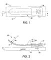
- Figs. 1, 2, 3, and 4 show a spring structure 100 according to a first embodiment of the present invention.
- Spring structure 100 generally includes a substrate 101, a support pad 110, a spring metal finger 120, and a stress-balancing pad 130.
- Substrate 101 e.g., glass
- conductor 105 may be an exposed portion of conducting material that is electrically connected to redistribution traces, through substrate vias, solder bumps, solder balls, mounted electrical components, integrated passive components, or interconnect pads.
- Support pad 110 is formed on an upper surface of substrate 101 such that it contacts conductor 105 (if present).
- support pad 110 is formed from a release material layer that is partially sacrificed to release a claw portion 125 of spring metal finger 120.
- support pad 110 may be titanium that is sputter deposited onto substrate 101 to a thickness of approximately 50 nm or greater. Titanium provides desirable characteristics as a release material layer due to its plasticity (i.e., its resistance to cracking). Other release materials having the beneficial plastic characteristics of titanium may also be used.
- support pad 110 includes another metal, such as Copper (Cu), Aluminum (Al), Nickel (Ni), Zirconium (Zr), or Cobalt (Co).
- support pad 110 provides electrical connection between spring metal finger 120 and conductor 105 (when present).
- support pad 110 may be formed from a non-conducting release material, and a strap or other conducting structure may be formed between spring metal finger and an exposed conductor.
- support portion 110 may be formed from a material different from the release material by separately patterning the release material and support portion 110 using known techniques.
- Spring metal finger 120 includes an anchor portion 122 and a claw (i.e., cantilevered portion) 125.
- Anchor portion 122 is attached to substrate 101 via support pad 110 (i.e., such that support pad 110 is located between anchor portion 122 and substrate 101).
- Claw 125 which includes a tip 125-T, extends from anchor portion 122 over substrate 101.
- Spring metal finger 120 is etched from a stress-engineered metal film that is deposited by DC magnetron sputtering one or more metals using gas (e.g., Argon) pressure variations in the sputter environment during film growth. These pressure variations are controlled using known techniques to generate an internal stress gradient that causes claw 125 to bend away from substrate 101 when an underlying release material is removed. Note that although much of this internal stress gradient is essentially relieved in the lifted claw 125, anchor portion 122 retains a substantial amount of internal stress.
- gas e.g., Argon
- the present inventors recognized that most failures of spring structures (i.e., separation of the spring structure from an underlying substrate through delamination or peeling) occur a significant amount of time after fabrication.
- stress-balancing pad 130 is formed on anchor portion 122 of spring metal finger 120 to counterbalance the internal stress gradient tending to separate (e.g., delaminate or peel) anchor portion 122 from support pad 110. Similar to spring metal finger 120, stress-balancing pad 130 is formed using a stress-engineered metal film that is deposited by DC magnetron sputtering one or more metals using gas pressure variations in the sputter environment during film growth. However, stress-balancing pad 130 is formed using a pressure variation sequence that is opposite to that utilized to generate spring metal finger 120, thereby causing stress-balancing pad 130 to include an internal stress that is opposite to that provided in spring metal finger 120.
- the opposite stress gradient is achieved by beginning the deposition process under conditions known to produce tensile stress, and then lowering the deposition sputter pressure in one or more steps to add one or more layers that are more compressive.
- the layers are engineered to produce a metal stack with zero net stress and zero net moment. Accordingly, stress-balancing pad 130 exerts a downward force (i.e., toward substrate 101) on the edges of anchor portion 122 that counterbalances the upward force generated by the internal stress gradient of spring metal finger 120, thereby resisting delamination or separation of anchor portion 122 from substrate 101.
- Fig. 4 is partial side view in which internal stress gradients are superimposed over portions of anchor portion 122 and stress-balancing pad 130.
- anchor portion 122 is etched from a stress-engineered metal film that has a positive stress gradient ⁇ + (i.e., tending to bend the edges of anchor portion 122 away from substrate 101)
- stress-balancing pad 130 is etched from a stress-engineered metal film that has a negative stress gradient ⁇ - (i.e., tending to bend the edges of stress-balancing pad 130 downward toward substrate 101).
- the negative stress gradient (and resulting stress moment) of stress-balancing pad 130 is equal in magnitude to or greater in magnitude than the positive stress gradient (and resulting stress moment) of anchor portion 122 such that zero net stress (and zero peeling moment) exists at an upper surface 131 of stress-balancing pad 130 is essentially nullified or slightly negative, thereby reliably preventing the separation of anchor portion 122.
- the stress gradient magnitude of stress-balancing pad 130 may be less than that of anchor portion 122 and still prolong the operational lifetime of spring structure 100 beyond that of conventional structures produced without stress-balancing pad 130.
- Figs. 5(A)-5(K), 6(A)-6(M), and 7(A)-7(L) are cross-sectional side views illustrating three methods for fabricating spring structures incorporating the stress-balancing pad of the present invention.
- both a spring metal layer and a stress-balancing layer are deposited/grown before the spring metal finger is processed (e.g., masked, etched and released).
- the first method requires a minimum number of processing steps, but typically requires forming the spring metal layer and the stress-balancing layer using different material compositions, and selectively etching a portion of the stress-balancing layer located over the claw portion of the spring metal finger.
- the first fabrication method begins with the formation of a release material layer 210 over a substrate 101 (e.g., silicon).
- release material layer 210 is formed from an electrically conductive material, and a portion 210A of release material layer 210 contacts a conductor 105 that is exposed on the upper surface of substrate 101.
- release material layer 210 is Titanium (Ti) that is sputter deposited onto substrate 101 to a thickness of approximately 0.2 microns or greater.
- Fig. 5(B) shows a stress-engineered spring metal layer 220 formed on release material layer 210 using known processing techniques such that it includes internal stress variations in the growth direction (i.e., as shown in Fig. 4).
- Methods for generating such internal stress variations in spring metal layer 220 are taught, for example, in US-A-3,842,189 (depositing two metals having different internal stresses) and US-A-5,613,861 (e.g., single metal sputtered while varying process parameters).
- spring metal layer 220 includes Molybdenum and Chromium (MoCr) sputter deposited to a thickness of 1 micron.
- a stress-balancing layer 230 is then formed on spring metal layer 220 using gas pressure variations that generate an internal stress gradient opposite to that of spring metal layer 220.
- Stress-balancing layer 230 is preferably formed from a material composition (e.g., Mo having a thickness of 1 micron) that is different from that utilized to form spring metal layer 2201. As discussed below, by forming stress-balancing layer 230 and spring metal layer 220 from different material compositions, selective etching may be utilized to remove portions of stress-balancing layer 230 without undesirably etching spring metal layer 220.
- Fig. 5(D) shows a spring metal (first) mask 240 (e.g., photoresist) that is patterned on a selected portion of stress-balancing layer 230. Note that spring metal mask 240 extends over an associated conductor 105 (if present).
- first mask 240 e.g., photoresist
- exposed portions of the stress-balancing layer and the spring metal layer surrounding mask 240 are etched using one or more etchants 242 to form a laminated structure including a stress-balancing island 230-1 on a spring metal island 220-1. Note that this etching process is selectively performed to minimize etching of release material layer 210 that surround spring metal island 220-1.
- a Mo stress-balancing layer and a MoCr spring metal layer are etched using a Cr etch, which does not significantly etch an underlying Ti release material layer.
- Fig. 5(F) shows a subsequent anisotropic etching process during which exposed portions of the release material layer surrounding spring metal island 220-1 are removed to form a release material island 210-1.
- anisotropic etching may be performed using fluorine plasma.
- the spring metal mask is then removed, and a release (second) mask 250 is formed that exposes a first portion 210-1A of the release material island, a first (claw) portion 220-1A of the spring metal island, and a first portion 230-1A of the stress-balancing island.
- release mask 250 is formed over a second portion 210-1B of the release material island, a second (anchor) portion 220-1B of the spring metal island, and a second portion 230-1B of the stress-balancing island, which, as described below, forms the stress-balancing pad of the present invention.
- an etchant 252 is then used to selectively etch the exposed first portion of the stress-balancing island, thereby forming stress-balancing pad 130.
- the stress-balancing layer is Mo and the spring metal layer is MoCr
- an anisotropic fluorine plasma etchant 252 is used, which does not etch claw portion 220-1B.
- a release etchant 254 e.g., a buffered oxide etch to remove Ti release material
- a release etchant 254 e.g., a buffered oxide etch to remove Ti release material
- removal of the exposed release material causes claw 125 to bend away from substrate 101 due to the internal stress variations established during the formation of the spring metal layer.
- anchor portion 122 remains attached to substrate 101 via support pad 110, which, along with stress-balancing pad 130, is protected during the release process by release mask 250.
- spring metal layer 220 (Fig. 5(B)) is formed using Nickel-Zirconium (NiZr), and stress-balancing layer 230 (Fig. 5(C)) is formed by Ti solution hardened with Si (Ti:Si).
- This alternative embodiment reduces fabrication costs by allowing the stress-balancing layer etch (Fig. 5(I)) and the release process (Fig. 5(J)) to be performed simultaneously using a single Ti etchant (e.g., a buffered oxide etch) that does not etch the NiZr claw portion of the spring metal finger.
- Figs. 6(A)-6(M) depict a second fabrication method that is similar to the first method in that a release material layer 310 (Fig. 6(A)), a spring metal layer 320 (Fig. 6(B)), and a stress-balancing layer 330 (Fig. 6(D)) are deposited/grown before the spring metal finger is processed.
- stress-balancing layer 330 and spring metal layer 320 are formed from the same material, thereby reducing the number of targets required in the deposition equipment, but requiring the deposition of an etch stop layer 325, as shown in Fig. 6(C), on spring metal layer 320 and sandwiched by the subsequently-formed stress-balancing layer 330 (shown in Fig. 6(D).
- One embodiment of the second method utilizes a Ti release layer 310, a Mo spring metal layer 320, a Cr etch stop layer 325, and a Mo stress-balancing layer 330.
- a spring metal (first) mask 340 is formed over stress-balancing layer 330 (Fig. 6(E)), and a first etchant (e.g., a Cr etch) 342 is utilized to form spring metal island 320-1, etch stop island 325-1, and stress-balancing island 330-1 (Fig. 6(F)).
- a second etchant 344 e.g., anisotropic etching using fluorine plasma
- etch the release material layer to form a release material island 310-1 (Fig. 6(G)
- the spring metal mask is removed (Fig. 6(H)).
- a release mask 350 is then formed that exposes a (first) portion 330-1 of the stress-balancing layer (Fig. 6(I)), and then this first portion is removed using etchant 352 (e.g., anisotropic etching using fluorine plasma; Fig. 6(J)).
- etchant 352 e.g., anisotropic etching using fluorine plasma; Fig. 6(J)
- An optional additional etchant 353 is then utilized, if necessary, to remove a portion 325-1A of the etch stop material form claw portion 320-1A (Figs. 6(J) and 6(K)), and then a release etchant 354 is utilized to release claw 125-A (Fig. 6(L)), which then forms a spring structure 100-A (Fig. 6(M)) having essentially the same characteristics described above with reference to Figs. 1-4.
- the single-step island formation etch (Fig. 6(F)) is replaced with a three-step process that includes forming the Mo stress-balancing island 330-1 by anisotropically etching the stress-balancing layer using fluorine plasma, forming Cr etch stop island 325-1 using a Cr etch, and then forming the Mo spring metal island 320-1 by anisotropically etching the spring metal layer using fluorine plasma.
- this alternative increases the number of etching steps, the feature definition of the resulting spring structure may be improved over that produced using the single-step island formation process described above.
- release material layer 310 (Fig. 6(A)) is formed using Si
- spring metal layer 320 (Fig. 6(B)) is formed using MoCr
- etch stop layer 325 (Fig. 6(C)) is formed using Ti
- stress-balancing layer 330 (Fig. 6(D)) is formed using MoCr.
- a three-step island formation process is utilized (Cr etch, Ti etch, Cr etch) to form stress-balancing island 330-1, etch stop island 325-1, and spring metal island 320-1, respectively.
- Portion 330-1A of stress-balancing island 320-1 is subsequently etched using a Cr etch, and release is performed using a Xenon-Fluoride (XeF 2 ) etchant 354.
- XeF 2 Xenon-Fluoride
- Figs. 7(A)-7(L) depict a third fabrication method in a (e.g., Ti) release material layer 410 (Fig. 7(A)) and a (e.g., MoCr) spring metal layer 420 (Fig. 7(B)) are formed, masked (Fig. 7(C)) and etched (Figs. 7(D) and 7(E)) before a (e.g., MoCr) stress-balancing layer is deposited. Specifically, after forming spring metal island 420-1 and release material island 410-1 (Figs. 7(D) and 7(E)), spring metal mask 440 is removed (Fig.
- a (second) mask 446 is formed that covers claw portion 420-1A and exposes anchor portion 420-1B (Fig. 7(G)).
- the stress-balancing layer is then deposited such that a first portions 430-1A is formed on mask 446, and a second portion 430-1B is formed on anchor portion 420-1B.
- Mask 446 is then lifted off along with first portions 430-1A (Fig. 7(I)) using known techniques to pattern stress-balancing pad 130-B, and then a release mask 450 is formed (Fig. 7(J)) that is utilized to release claw 125-B (Fig. 7(K)), and is then removed (Fig. 7(L)) to complete the fabrication of a spring structure 100-B having essentially the same characteristics described above with reference to Figs. 1-4.
- three masks may be utilized to form the spring structure such that the stress balancing pad is formed before the spring metal island is etched.
- a release material layer, a spring metal layer, and a stress balancing layer are sequentially deposited (i.e., forming a structure similar to that shown in Figs. 5(C) and 6(C)).
- a first mask is then patterned and used to etch only the stress balancing layer according to known techniques, thereby forming the stress balancing pad.
- the spring metal layer and release layer are then etched using a second mask (i.e., similar to that shown in Figs. 5(D) and 6(D)) to form the spring metal and release material islands.
- a release mask i.e., similar to that shown in Figs. 5(H) and 6(I) is then used to etch release material located under the claw portion to release the claw.
- An intermediate etch stop layer may also be formed between the spring metal layer and the stress balancing layer in the manner described above.
- the disclosed process examples are not intended to be limited to the specific fabrication processes and material compositions. Other structures such as passivating layers, capping layers, devices, vias etc., may be incorporated in the process flow. Further, the described embodiments utilize two layers having opposing gradients (i.e., the spring metal layer and the stress-balancing layer). However, spring structures exhibiting the same stress-nullifying benefits of the disclosed embodiments may be produced with other stress profiles (e.g., a series of stress-engineered layers that are compressive, tensile then compressive again).
Landscapes
- Engineering & Computer Science (AREA)
- Physics & Mathematics (AREA)
- General Physics & Mathematics (AREA)
- Manufacturing & Machinery (AREA)
- Microelectronics & Electronic Packaging (AREA)
- Micromachines (AREA)
- Wire Bonding (AREA)
- Magnetic Heads (AREA)
- Measuring Leads Or Probes (AREA)
Abstract
Description
Claims (8)
- A spring structure (100) comprising:a substrate (101);a spring metal finger (120) including an unlifted anchor portion (122) attached to the substrate (101) and a released claw portion (125) extending over the substrate (101), wherein the anchor portion (122) has a first internal stress gradient; anda stress-balancing pad (130) formed on the anchor portion (122) of the spring metal finger (120), wherein the stress-balancing pad (130) has a second internal stress gradient that is opposite to the first internal stress gradient.
- A spring structure according to Claim 1, wherein the second internal stress gradient of the stress-balancing pad (130) is equal in magnitude to or greater in magnitude than the first internal stress gradient of the anchor portion (122).
- A spring structure according to Claim 1 or 2, wherein both the spring metal finger (120) and the stress-balancing pad (130) consist essentially of a single material composition.
- A spring structure according to Claim 3, wherein the single material composition is Molybdenum (Mo) or Molybdenum-Chromium (MoCr).
- A spring structure according to Claim 1 or 2, wherein the spring metal finger (120) comprises a first material, and wherein the stress-balancing pad (130) comprises a second material that is different from the first material.
- A spring structure according to Claim 5, wherein the first material consists essentially of a Molybdenum-Chromium alloy (MoCr), and wherein the stress-balancing pad (130) consists essentially of Molybdenum (Mo).
- A spring structure comprising:wherein the spring metal finger is formed from a first stress-engineered material having a first internal stress moment that causes the claw portion to bend away from the substrate, anda substrate;a spring metal finger having an anchor portion supported by the substrate and a claw portion extending over the substrate; anda stress-balancing pad formed over the anchor portion of the spring metal finger,
wherein the stress-balancing pad is formed from a second stress-engineered material having a second internal moment that opposes to the first internal stress moment. - A method for fabricating a spring structure (100) on a substrate (107), the method comprising:forming a spring metal island (220) on a release material island (210) such that the spring metal island (220) has a first internal stress;forming a stress-balancing pad (130) only over an anchor portion (122) of the spring metal island (220), wherein the stress-balancing pad (130) has a second internal stress that is opposite to the first internal stress; and,selectively removing a portion of the release material island (210) located under a claw portion (125) of the spring metal island (220) such that the claw portion (125) bends away from the substrate and the anchor portion (122) remains attached to the substrate (107).
Applications Claiming Priority (2)
| Application Number | Priority Date | Filing Date | Title |
|---|---|---|---|
| US09/976,394 US6794737B2 (en) | 2001-10-12 | 2001-10-12 | Spring structure with stress-balancing layer |
| US976394 | 2001-10-12 |
Publications (3)
| Publication Number | Publication Date |
|---|---|
| EP1304768A2 true EP1304768A2 (en) | 2003-04-23 |
| EP1304768A3 EP1304768A3 (en) | 2004-02-04 |
| EP1304768B1 EP1304768B1 (en) | 2005-09-14 |
Family
ID=25524048
Family Applications (1)
| Application Number | Title | Priority Date | Filing Date |
|---|---|---|---|
| EP02256864A Expired - Lifetime EP1304768B1 (en) | 2001-10-12 | 2002-10-02 | Spring structure |
Country Status (4)
| Country | Link |
|---|---|
| US (1) | US6794737B2 (en) |
| EP (1) | EP1304768B1 (en) |
| JP (1) | JP4427239B2 (en) |
| DE (1) | DE60206121T2 (en) |
Cited By (2)
| Publication number | Priority date | Publication date | Assignee | Title |
|---|---|---|---|---|
| EP1480335A3 (en) * | 2003-05-22 | 2004-12-01 | Samsung Electronics Co., Ltd. | Method of manufacturing film bulk acoustic resonator using internal stress of metallic film and resonator manufactured thereby |
| FR2859201A1 (en) * | 2003-08-29 | 2005-03-04 | Commissariat Energie Atomique | MICROMECHANICAL DEVICE COMPRISING A SUSPENDED ELEMENT ATTACHED TO A SUPPORT BY A PILLAR AND METHOD OF MANUFACTURING SUCH A DEVICE |
Families Citing this family (14)
| Publication number | Priority date | Publication date | Assignee | Title |
|---|---|---|---|---|
| US7410590B2 (en) * | 2003-12-19 | 2008-08-12 | Palo Alto Research Center Incorporated | Transferable micro spring structure |
| CA2563406C (en) * | 2004-04-23 | 2013-09-17 | Research Triangle Institute | Flexible electrostatic actuator |
| US7262495B2 (en) * | 2004-10-07 | 2007-08-28 | Hewlett-Packard Development Company, L.P. | 3D interconnect with protruding contacts |
| US7550855B2 (en) * | 2005-12-02 | 2009-06-23 | Palo Alto Research Center Incorporated | Vertically spaced plural microsprings |
| US20090140433A1 (en) * | 2007-11-30 | 2009-06-04 | Alces Technology, Inc. | MEMS chip-to-chip interconnects |
| TWI404428B (en) * | 2009-11-25 | 2013-08-01 | Ind Tech Res Inst | Acoustics transducer |
| US8579414B2 (en) * | 2009-12-23 | 2013-11-12 | Xerox Corporation | Self-assembling structures for electrostatic extraction of pigments from liquid inks for marking |
| US8519534B2 (en) | 2010-09-22 | 2013-08-27 | Palo Alto Research Center Incorporated | Microsprings partially embedded in a laminate structure and methods for producing same |
| US8441808B2 (en) | 2010-09-22 | 2013-05-14 | Palo Alto Research Center Incorporated | Interposer with microspring contacts |
| CN102305256B (en) * | 2011-09-06 | 2013-06-12 | 复旦大学 | Metal micrometer/nanometer spring as well as preparation method and application thereof |
| US8525353B2 (en) | 2011-12-19 | 2013-09-03 | Palo Alto Research Center Incorporated | Microspring structures adapted for target device cooling |
| CN104555908A (en) * | 2014-12-04 | 2015-04-29 | 复旦大学 | Machining method of micro-spring |
| US11434130B2 (en) | 2019-12-31 | 2022-09-06 | Texas Instruments Incorporated | Surface micromachined structures |
| US12224082B2 (en) * | 2023-02-09 | 2025-02-11 | Xerox Corporation | Stress engineered microspring for cryogenic superconducting circuits |
Family Cites Families (6)
| Publication number | Priority date | Publication date | Assignee | Title |
|---|---|---|---|---|
| US3842189A (en) * | 1973-01-08 | 1974-10-15 | Rca Corp | Contact array and method of making the same |
| US5613861A (en) * | 1995-06-07 | 1997-03-25 | Xerox Corporation | Photolithographically patterned spring contact |
| US6236491B1 (en) * | 1999-05-27 | 2001-05-22 | Mcnc | Micromachined electrostatic actuator with air gap |
| US6290510B1 (en) * | 2000-07-27 | 2001-09-18 | Xerox Corporation | Spring structure with self-aligned release material |
| US6528250B1 (en) * | 2000-09-09 | 2003-03-04 | Akzo Nobel N.V. | Equine infectious anemia challenge model for testing vaccines, diagnostics and treatments |
| US6560861B2 (en) * | 2001-07-11 | 2003-05-13 | Xerox Corporation | Microspring with conductive coating deposited on tip after release |
-
2001
- 2001-10-12 US US09/976,394 patent/US6794737B2/en not_active Expired - Lifetime
-
2002
- 2002-10-02 DE DE60206121T patent/DE60206121T2/en not_active Expired - Lifetime
- 2002-10-02 EP EP02256864A patent/EP1304768B1/en not_active Expired - Lifetime
- 2002-10-08 JP JP2002294382A patent/JP4427239B2/en not_active Expired - Fee Related
Cited By (5)
| Publication number | Priority date | Publication date | Assignee | Title |
|---|---|---|---|---|
| EP1480335A3 (en) * | 2003-05-22 | 2004-12-01 | Samsung Electronics Co., Ltd. | Method of manufacturing film bulk acoustic resonator using internal stress of metallic film and resonator manufactured thereby |
| US7671427B2 (en) | 2003-05-22 | 2010-03-02 | Samsung Electronics Co., Ltd. | Method of manufacturing film bulk acoustic resonator using internal stress of metallic film and resonator manufactured thereby |
| US7939356B2 (en) | 2003-05-22 | 2011-05-10 | Samsung Electronics Co., Ltd. | Method of manufacturing film bulk acoustic resonator using internal stress of metallic film and resonator manufactured thereby |
| FR2859201A1 (en) * | 2003-08-29 | 2005-03-04 | Commissariat Energie Atomique | MICROMECHANICAL DEVICE COMPRISING A SUSPENDED ELEMENT ATTACHED TO A SUPPORT BY A PILLAR AND METHOD OF MANUFACTURING SUCH A DEVICE |
| US7671429B2 (en) | 2003-08-29 | 2010-03-02 | Commissariat A L'energie Atomique | Micro-mechanical device comprising suspended element which is connected to a support by means of a pier and producing method thereof |
Also Published As
| Publication number | Publication date |
|---|---|
| DE60206121D1 (en) | 2005-10-20 |
| US20030071330A1 (en) | 2003-04-17 |
| US6794737B2 (en) | 2004-09-21 |
| EP1304768A3 (en) | 2004-02-04 |
| JP4427239B2 (en) | 2010-03-03 |
| JP2003218292A (en) | 2003-07-31 |
| EP1304768B1 (en) | 2005-09-14 |
| DE60206121T2 (en) | 2006-05-04 |
Similar Documents
| Publication | Publication Date | Title |
|---|---|---|
| US6528350B2 (en) | Method for fabricating a metal plated spring structure | |
| EP1277696B1 (en) | Spring with conductive coating | |
| US6684499B2 (en) | Method for fabricating a spring structure | |
| EP1304768B1 (en) | Spring structure | |
| US6290510B1 (en) | Spring structure with self-aligned release material | |
| JP3386077B2 (en) | Probe card assemblies and kits and methods of using them | |
| EP1746869B1 (en) | Methods for embedding conducting material and devices resulting from said methods | |
| US8575954B2 (en) | Structures and processes for fabrication of probe card assemblies with multi-layer interconnect | |
| US7985081B2 (en) | Transferable micro spring structure | |
| TW200905991A (en) | Method and system for batch manufacturing of spring elements | |
| US7015584B2 (en) | High force metal plated spring structure | |
| EP1255295A1 (en) | Semiconductor device, metal laminated plate for fabricating circuit on semiconductor, and method of fabricating circuit | |
| US20060087335A1 (en) | Curved spring structure with elongated section located under cantilevered section | |
| US20040137707A1 (en) | Flat-top bumping structure and preparation method | |
| KR20070043856A (en) | Interconnect Assemblies and Methods | |
| EP1950851A1 (en) | Spiral contact and process for producing the same |
Legal Events
| Date | Code | Title | Description |
|---|---|---|---|
| PUAI | Public reference made under article 153(3) epc to a published international application that has entered the european phase |
Free format text: ORIGINAL CODE: 0009012 |
|
| AK | Designated contracting states |
Designated state(s): AT BE BG CH CY CZ DE DK EE ES FI FR GB GR IE IT LI LU MC NL PT SE SK TR |
|
| AX | Request for extension of the european patent |
Extension state: AL LT LV MK RO SI |
|
| PUAL | Search report despatched |
Free format text: ORIGINAL CODE: 0009013 |
|
| AK | Designated contracting states |
Kind code of ref document: A3 Designated state(s): AT BE BG CH CY CZ DE DK EE ES FI FR GB GR IE IT LI LU MC NL PT SE SK TR |
|
| AX | Request for extension of the european patent |
Extension state: AL LT LV MK RO SI |
|
| RIC1 | Information provided on ipc code assigned before grant |
Ipc: 7B 81B 3/00 B Ipc: 7H 01R 13/22 A |
|
| 17P | Request for examination filed |
Effective date: 20040804 |
|
| AKX | Designation fees paid |
Designated state(s): DE FR GB |
|
| 17Q | First examination report despatched |
Effective date: 20041217 |
|
| GRAP | Despatch of communication of intention to grant a patent |
Free format text: ORIGINAL CODE: EPIDOSNIGR1 |
|
| GRAS | Grant fee paid |
Free format text: ORIGINAL CODE: EPIDOSNIGR3 |
|
| GRAA | (expected) grant |
Free format text: ORIGINAL CODE: 0009210 |
|
| AK | Designated contracting states |
Kind code of ref document: B1 Designated state(s): DE FR GB |
|
| REG | Reference to a national code |
Ref country code: GB Ref legal event code: FG4D |
|
| REF | Corresponds to: |
Ref document number: 60206121 Country of ref document: DE Date of ref document: 20051020 Kind code of ref document: P |
|
| ET | Fr: translation filed | ||
| PLBE | No opposition filed within time limit |
Free format text: ORIGINAL CODE: 0009261 |
|
| STAA | Information on the status of an ep patent application or granted ep patent |
Free format text: STATUS: NO OPPOSITION FILED WITHIN TIME LIMIT |
|
| 26N | No opposition filed |
Effective date: 20060615 |
|
| REG | Reference to a national code |
Ref country code: FR Ref legal event code: PLFP Year of fee payment: 15 |
|
| REG | Reference to a national code |
Ref country code: FR Ref legal event code: PLFP Year of fee payment: 16 |
|
| REG | Reference to a national code |
Ref country code: FR Ref legal event code: PLFP Year of fee payment: 17 |
|
| PGFP | Annual fee paid to national office [announced via postgrant information from national office to epo] |
Ref country code: FR Payment date: 20190919 Year of fee payment: 18 |
|
| PGFP | Annual fee paid to national office [announced via postgrant information from national office to epo] |
Ref country code: GB Payment date: 20190923 Year of fee payment: 18 |
|
| PGFP | Annual fee paid to national office [announced via postgrant information from national office to epo] |
Ref country code: DE Payment date: 20190918 Year of fee payment: 18 |
|
| REG | Reference to a national code |
Ref country code: DE Ref legal event code: R119 Ref document number: 60206121 Country of ref document: DE |
|
| GBPC | Gb: european patent ceased through non-payment of renewal fee |
Effective date: 20201002 |
|
| PG25 | Lapsed in a contracting state [announced via postgrant information from national office to epo] |
Ref country code: DE Free format text: LAPSE BECAUSE OF NON-PAYMENT OF DUE FEES Effective date: 20210501 Ref country code: FR Free format text: LAPSE BECAUSE OF NON-PAYMENT OF DUE FEES Effective date: 20201031 |
|
| PG25 | Lapsed in a contracting state [announced via postgrant information from national office to epo] |
Ref country code: GB Free format text: LAPSE BECAUSE OF NON-PAYMENT OF DUE FEES Effective date: 20201002 |