EP1304720A1 - Photomultiplier tube, photomultiplier tube unit, radiation detector - Google Patents
Photomultiplier tube, photomultiplier tube unit, radiation detector Download PDFInfo
- Publication number
- EP1304720A1 EP1304720A1 EP00922982A EP00922982A EP1304720A1 EP 1304720 A1 EP1304720 A1 EP 1304720A1 EP 00922982 A EP00922982 A EP 00922982A EP 00922982 A EP00922982 A EP 00922982A EP 1304720 A1 EP1304720 A1 EP 1304720A1
- Authority
- EP
- European Patent Office
- Prior art keywords
- photomultiplier tube
- stem plate
- photomultiplier
- circuit board
- stem
- Prior art date
- Legal status (The legal status is an assumption and is not a legal conclusion. Google has not performed a legal analysis and makes no representation as to the accuracy of the status listed.)
- Granted
Links
- 230000005855 radiation Effects 0.000 title claims abstract description 21
- 125000006850 spacer group Chemical group 0.000 claims description 35
- 239000011521 glass Substances 0.000 claims description 30
- 229910052751 metal Inorganic materials 0.000 claims description 22
- 239000002184 metal Substances 0.000 claims description 22
- 239000000758 substrate Substances 0.000 claims description 12
- 239000012777 electrically insulating material Substances 0.000 claims description 9
- 230000004044 response Effects 0.000 claims description 6
- 239000000463 material Substances 0.000 claims description 3
- 230000006335 response to radiation Effects 0.000 claims description 2
- 238000003780 insertion Methods 0.000 description 11
- 230000037431 insertion Effects 0.000 description 11
- 238000003466 welding Methods 0.000 description 10
- 238000000034 method Methods 0.000 description 8
- 230000007257 malfunction Effects 0.000 description 6
- 230000000694 effects Effects 0.000 description 5
- 229910000833 kovar Inorganic materials 0.000 description 5
- 239000002585 base Substances 0.000 description 4
- 230000003247 decreasing effect Effects 0.000 description 3
- 239000011159 matrix material Substances 0.000 description 3
- 238000003825 pressing Methods 0.000 description 3
- 229910001220 stainless steel Inorganic materials 0.000 description 3
- 239000010935 stainless steel Substances 0.000 description 3
- 229910052783 alkali metal Inorganic materials 0.000 description 2
- 150000001340 alkali metals Chemical class 0.000 description 2
- 230000017525 heat dissipation Effects 0.000 description 2
- 238000004519 manufacturing process Methods 0.000 description 2
- 239000007769 metal material Substances 0.000 description 2
- 238000009206 nuclear medicine Methods 0.000 description 2
- 239000000853 adhesive Substances 0.000 description 1
- 230000001070 adhesive effect Effects 0.000 description 1
- 229910052787 antimony Inorganic materials 0.000 description 1
- WATWJIUSRGPENY-UHFFFAOYSA-N antimony atom Chemical compound [Sb] WATWJIUSRGPENY-UHFFFAOYSA-N 0.000 description 1
- 239000000919 ceramic Substances 0.000 description 1
- 238000009826 distribution Methods 0.000 description 1
- 238000010894 electron beam technology Methods 0.000 description 1
- 230000004927 fusion Effects 0.000 description 1
- 238000007499 fusion processing Methods 0.000 description 1
- 238000010438 heat treatment Methods 0.000 description 1
- 238000003384 imaging method Methods 0.000 description 1
- 230000001678 irradiating effect Effects 0.000 description 1
- 239000000155 melt Substances 0.000 description 1
- 239000011347 resin Substances 0.000 description 1
- 229920005989 resin Polymers 0.000 description 1
- 230000035945 sensitivity Effects 0.000 description 1
Images





Classifications
-
- H—ELECTRICITY
- H01—ELECTRIC ELEMENTS
- H01J—ELECTRIC DISCHARGE TUBES OR DISCHARGE LAMPS
- H01J43/00—Secondary-emission tubes; Electron-multiplier tubes
- H01J43/04—Electron multipliers
- H01J43/045—Position sensitive electron multipliers
-
- H—ELECTRICITY
- H01—ELECTRIC ELEMENTS
- H01J—ELECTRIC DISCHARGE TUBES OR DISCHARGE LAMPS
- H01J43/00—Secondary-emission tubes; Electron-multiplier tubes
- H01J43/04—Electron multipliers
- H01J43/28—Vessels, e.g. wall of the tube; Windows; Screens; Suppressing undesired discharges or currents
Definitions
- the present invention relates to a photomultiplier tube for detecting weak light incident on a faceplate by multiplying electrons emitted from the faceplate, a photomultiplier tube unit including photomultiplier tubes, and a radiation detector employing photomultiplier tubes and/or photomultiplier tube units.
- Japanese patent application Kokai publication No. 5-100034 discloses a scintillation camera wherein photomultiplier tubes are closely arranged together on a top surface of a scintillator. Sockets of the photomultiplier tubes are used for mounting the photomultiplier tubes onto the scintillator. A spiral spring is disposed around each socket, connecting each photomultiplier tube with a pressing plate facing the scintillator. A photocathode of the photomultiplier tube is pressed to the scintillator and fixed thereon by the spiral spring. In this way, a predetermined spring force is used to fix each photomultiplier tube on the scintillator.
- a photomultiplier tube includes a photocathode for emitting electrons in response to light incident on a faceplate; an electron multiplier provided in an hermetically sealed vessel for multiplying electrons emitted from the photocathode; and an anode for generating an output signal based on electrons multiplied by the electron multiplier.
- the photomultiplier tube is characterized by the hermetically sealed vessel including a stem plate having stem pins for fixing the electron multiplier and the anode thereon; a metal side tube enclosing the electron multiplier and the anode, the metal side tube having an open end to which the stem plate is fixed; and the faceplate fixed to another open end of the side tube.
- the faceplate is made from glass. Screw means is provided at a lower surface of the stem plate.
- the photomultiplier tube of the present invention simplifies the process of fixing the hermetically sealed vessel to a predetermined location by using screws.
- photomultiplier tubes are not provided with its own special fixing structure in order to enhance its flexibility.
- due to increased sensitivity properties of photomultiplier tubes in recent years there have been more opportunities for incorporating such photomultiplier tubes in various devices.
- the operations required for mounting and replacing individual photomultiplier tubes in such equipment requires proficiency.
- screw means is provided on the stem plate of the photomultiplier tube according to the present invention.
- the screw means includes a spacer projecting from the lower surface of the stem plate.
- the spacer has a female thread in the interior thereof.
- the stem plate When a photomultiplier tube having the above structure is mounted at a predetermined position, the stem plate can be fixed in place while still maintaining spaced away from the mounting area by the spacer, thereby encouraging heat dissipation from the stem plate and contributing to improved performance of the photomultiplier tube. Further, by forming the spacer of an electrically insulating material, it is possible to prevent electrical effects of the photomultiplier tube operating at a high voltage from being transferred externally.
- the photomultiplier tube according to present invention further includes a circuit board extending parallel to the stem plate and electrically connected to the stem pins.
- the circuit board is secured to the stem plate by screwing a male screw into the screw means.
- the circuit board is integrally attached to the photomultiplier tube be means of the male screws.
- the photomultiplier tube according to present invention may further include a first circuit board detachably provided with the stem plate.
- the first circuit board may be secured to the stem plate by screwing a screw member into the screw means through the first circuit board. If the screwing means has female threads, male screws are used as the screw member to fix the first circuit board to the stem plate. If the screwing means has male screws, nuts having female threads are used as the screw member for fixing the first circuit board to the stem plate.
- the screw means may include a spacer projecting from the lower surface of the stem plate.
- the spacer is integral with the stem plate by using the same material as that of the stem plate.
- the spacer spaces the first circuit board away from the stem plate.
- the screw member may be made from an electrically insulating material.
- the screw means may include a spacer projecting from the lower surface of the stem plate.
- the spacer is made from an electrically insulating material. The spacer spaces the first circuit board away from the stem plate.
- the screw member made from an electrically insulating material is preferably used.
- the photomultiplier tube according to present invention may further include a second circuit board detachably provided with the stem plate and the first circuit board.
- the first and second circuit boards may be secured to the stem plate by screwing the screw member into the screw means through the first and second circuit boards.
- a photomultiplier tube unit includes a plurality of photomultiplier tubes that are juxtaposed, each of the plurality of the photomultiplier tubes having a photocathode for emitting electrons in response to light incident on a faceplate; an electron multiplier provided in an hermetically sealed vessel for multiplying electrons emitted from the photocathode; and an anode for generating an output signal based on electrons multiplied by the electron multiplier.
- the hermetically sealed vessel includes: a stem plate having stem pins for fixing the electron multiplier and the anode thereon; a metal side tube enclosing the electron multiplier and the anode, the side tube having one open end to which the stem plate is fixed; and the faceplate fixed to another open end of the side tube.
- the faceplate is made from glass. Screw means is provided on a lower surface of the stem plate.
- photomultiplier tube unit it is possible to arrange a plurality of photomultiplier tubes on a single circuit board using male screw members.
- This structure enables the photomultiplier tubes to be modularized with the simple operation of inserting screws.
- these photomultiplier tubes can be easily incorporated into a variety of equipment.
- the substrate is a circuit board electrically connectable to the stem pins.
- the male screw members are electrically insulating screws.
- a radiation detector includes a scintillator for emitting fluorescent light in response to radiation generated from an object; a plurality of photomultiplier tubes arranged in a manner that faceplates of the photomultiplier tubes face the scintillator. Each of the photomultiplier tubes generates an electrical charge based on the fluorescent light emitted from the scintillator.
- the radiation detector includes a position calculating processor for processing an output from the photomultiplier tube and generating a signal for indicating a position of radiation generated in the object.
- Each of the plurality of photomultiplier tubes has a photocathode for emitting electrons in response to light incident on a faceplate; an electron multiplier provided in an hermetically sealed vessel for multiplying electrons emitted from the photocathode; and an anode for producing an output signal based on electrons multiplied by the electron multiplier.
- the hermetically sealed vessel includes: a stem plate having stem pins for securing the electron multiplier and the anode; a metal side tube for enclosing the electron multiplier and the anode, the side tube having one open end to which the stem plate is fixed; and the faceplate fixed to another open end of the side tube, the faceplate being made from glass. Screw means is provided at a lower surface of the stem plate.
- the hermetically sealed vessels are arranged to be secured to a single substrate by screwing male screws into the screw mean members while the hermetically sealed vessels are juxtaposed on the substrate.
- the radiation detector employs units including a plurality of photomultiplier tubes arranged on a single circuit board and fixed by male screw members, a complex process is not required when replacing individual photomultiplier tubes in radiation detectors (such as a gamma camera) in which a plurality of photomultiplier tubes are incorporated. Replacement operations can be performed on individual units. Therefore, the time required for the replacement operation is reduced. Moreover, by employing a structure using screws, it is possible to facilitate the operation for attaching and detaching each photomultiplier tube in relation to the circuit board and for replacing individual photomultiplier tubes in the detached units.
- Fig. 1 is a perspective view showing a photomultiplier tube according to the present invention.
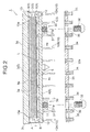
- Fig. 2 is a cross-sectional view of the photomultiplier tube in Fig. 1.
- the photomultiplier tube 1 includes a side tube 2 having a substantially rectangular section and formed from a metal material (such as Kovar metal and stainless steel).
- a glass faceplate 3 is fused to one open end A of the side tube 2.
- a photocathode 3a for converting light to an electron is formed on an inner surface of the faceplate 3.
- the photocathode 3a is formed by reacting alkali metal vapor with antimony pre-deposited on the faceplate 3.
- a stem plate 4 made from a metal material (such as Kovar metal and stainless steel) is welded to the other open end B of the side tube 2.
- the assembly of the side tube 2, faceplate 3, and stem plate 4 forms a hermetically sealed vessel 5.
- the vessel 5 has a low height of approximately 10 mm.
- a metal evacuating tube 6 is provided in the center of the stem plate 4.
- the evacuating tube 6 is used to evacuate the vessel 5 by a vacuum pump (not shown) after the assembly of the photomultiplier tube 1 is over.
- the evacuating tube 6 is also used for introducing alkali metal vapor into the vessel 5 during the production of the photocathode 3a.
- a stacked electron multiplier 7 in a block shape is disposed inside the vessel 5.
- the electron multiplier 7 has an electron multiplying section 9 in which ten stages of flat dynodes 8 are stacked.
- Stem pins 10 formed from Kovar metal penetrate the stem plate 4 and support the electron multiplier 7 in the vessel 5.
- the tip of each stem pin 10 is electrically connected to each dynode 8.
- Pinholes 4a are formed in the stem plate 4, enabling the stem pins 10 to penetrate the stem plate 4.
- Each of the pinholes 4a is filled with a tablet 11 formed from Kovar glass, which forms a hermetic seal between the stem pins 10 and the stem plate 4.
- Each stem pin 10 is fixed to the stem plate 4 by the tablet 11.
- the stem pins 10 are classified into two groups: one group for dynode pins 10A connected individually to each dynode 8, and the other group for anode pins 10B connected individually to each of anodes 12 described later.
- the anodes 12 are positioned below the electron multiplying section 9 in the electron multiplier 7.
- the anodes 12 are fixed to the top ends of the anode pins 10B.
- a flat focusing electrode 13 is disposed between the photocathode 3a and the electron multiplying section 9 above the top stage of the electron multiplier 7.
- a plurality of slit-shaped openings 13a is formed in the focusing electrode plate 13.
- the openings 13a are arranged parallel to each other with respect to one direction.
- Slit-shaped electron multiplying holes 8a are formed in the dynode 8.
- the number of electron multiplying holes 8a is the same as that of the openings 13a.
- the electron multiplying holes 8a are arranged parallel to each other in one direction.
- the electron multiplying holes 8a extend in a direction substantially orthogonal to the surface of the dynodes 8.
- Electron multiplying paths L are formed by arranging the electron multiplying holes 8a in each dynode 8 along the direction of the stack.
- a plurality of channels are formed in the electron multiplier 7 by associating the path L with the corresponding opening 13a in the focusing electrode plate 13.
- the anodes 12 are configured in an 8x8 arrangement, so that each anode 12 corresponds to a predetermined number of channels. Since the anode 12 is connected to the corresponding anode pin 10B, output signals can be extracted through each anode pin 10B.
- the electron multiplier 7 has a plurality of linear channels.
- a predetermined voltage is applied across the electron multiplying section 9 and anodes 12 by the stem pin 10 connected to a bleeder circuit (not shown).
- the photocathode 3a and the focusing electrode plate 13 are maintained at the same potential.
- the potential of each dynode is decreasing from the top of the dynode toward the anodes 12. Accordingly, incident light on the faceplate 3 is converted to electrons at the photocathode 3a.
- the electrons are guided into a certain channel by the electron lens effect generated by the focusing electrode plate 13 and the first stage of the dynode 8 on the top of the electron multiplier 7.
- the electrons guided into the channel are multiplied through each stage of the dynodes 8 while passing through the electron multiplying paths L.
- the electrons are collected by the anodes 12 to be outputted as an output signal.
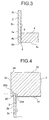
- the stem plate 4 is brought into contact with the open end B of the side tube 2 such that a side face 4b of the stem plate 4 contacts an inner surface 2c in the vicinity of a lower end 2a of the side tube 2.
- a lower end face 2d of the side tube 2 is approximately flush with a lower face 4c of the stem plate 4 in order that the lower end surface 2d does not project below the stem plate 4.
- the above structure extends the lower end 2a of the side tube 2 in the substantial axial direction of the tube 2, and eliminates lateral projection like a flange at the lower end of the photomultiplier tube 1.
- a junction F between the side tube 2 and stem plate 4 is laser-welded by irradiating a laser beam on the junction F from a point directly below and external to the junction F or in a direction toward the junction F.
- the above laser welding is one example for fusing the stem plate 4 and side tube 2.
- the side tube 2 and the stem plate 4 are welded together using the laser welding, it is unnecessary to apply pressure across the junction F between the side tube 2 and stem plate 4 in contrast to resistance welding. Hence, no residual stress is induced at the junction F, avoiding cracks from occurring at this junction during the usage.
- the usage of the laser welding greatly improves the durability and sealability of the photomultiplier tube 1.
- Laser welding and electron beam welding prevent generation of heat at the junction F, compared to the resistance welding. Hence, when the photomultiplier tube 1 is assembled, there is very little effect of heat on the components in the vessel 5.
- the side tube 2 is formed by pressing a flat plate made from metal such as Kovar and stainless steel into an approximately rectangular cylindrical shape having a thickness of approximately 0.25 mm and a height of approximately 7 mm.
- the glass faceplate 3 is fixed to the open end A of the side tube 2 by fusion.
- an edge portion 20 is formed on an upper end of the side tube 2 which the glass faceplate 3 faces.
- the edge portion 20 is provided around the whole upper end of the side tube 2.
- the edge portion 20 curves outwardly with a curved part 20a formed on an inner surface 2c side of the side tube 2.
- a tip 20b of the edge portion 20 is formed like a knife-edge.
- the metal side tube 2 is placed on a rotating platform (not shown) with the bottom surface of the glass faceplate 3 contacting the tip 20b of the edge portion 20.
- the side tube 2 is heated by a high-frequency heating device while the glass faceplate 3 is pressed downwardly by a pressure jig.
- the heated edge portion 20 gradually melts the glass faceplate 3, and penetrates therein.
- the edge portion 20 is brought into embedded in the glass faceplate 3, ensuring a tight seal at the juncture between the glass faceplate 3 and side tube 2.
- the edge portion 20 extends upwardly from the side tube 2 rather than extends laterally from the side tube 2 like a flange.
- an overhanging part 3A having a predetermined length of extension is formed in the glass faceplate 3, expanding the effective surface area of a photocathode 3d formed on the glass faceplate 3.
- the above fusing method for fusing glass and metal is employed due to the combination of metal and glass.
- the overhanging part 3A of the glass faceplate 3 functions extremely effectively to ensure a fusing area necessary to fuse the glass faceplate 3 and side tube 2. The increase of the amount of overhang in the overhanging part 3A avoids the side surface 3c from deformating during the fusion process, allowing the side surface 3c to retain its form throughout the process.
- the photomultiplier tube 1 has four threaded portions 30.
- Each threaded portion 30 is provided in each corner of the stem plate 4.
- the threaded portion 30 includes a cylindrical spacer 31 projecting from the lower surface 4c of the stem plate 4.
- the cylindrical spacer 31 has a female threaded hole 31a therein.
- the cylindrical spacer 31 is made from the same material as that of the stem plate 4, and integrally molded with the stem plate 4.
- the cylindrical spacer 31 may be made from electrically insulating material such as resin separately from the stem plate 4.
- the vessel 5 can be easily mounted at a predetermined position. Additionally, standardization of the threaded portions 30 may contribute to standardizing a method for fixing the photomultiplier tube 1. For example, when a photomultiplier tube 1 in a photodetector malfunctions, a photomultiplier tube 1 having the same standard specifications can be easily installed at the same position in a correct manner in the photodetector.
- the stem plate 4 is spaced away from the substrate by the cylindrical spacer 31.
- the above structure ensures heat dissipation from the stem plate 4, and contributes to the enhanced performance of the photomultiplier tube 1.
- the cylindrical spacer 31 is formed from an electrically insulating material, it is possible to prevent the electrical effects of the possible to prevent the electrical effects of the photomultiplier tube 1 operating at a high voltage from being transferred externally.
- a voltage dividing circuit which is connectable to the dynode pins 10A, or a first circuit board 33 which is connectable to the anode pins 10B and has circuit patterns for anode output may be fixed to the photomultiplier tube 1.
- the first circuit board 33 has metal socket pins 34 corresponding to the anode pins 10B and metal socket pins 35 corresponding to the dynode pins 10A.
- An evacuating tube insertion hole 33a for inserting the evacuating tube 6 is formed in the center of the first circuit board 33.
- Screw insertion holes 36 are formed in the first circuit board 33 at positions corresponding to the spacers 31. After the anode pins 10B and dynode pins 10A are inserting into the socket pins 34 and socket pins 35, and the screw insertion holes 36 is aligned with the female thread 31a of the spacers 31, electrical insulated screws 32 (male screws) are screwed into the female threaded holes 31a from below, thereby fixing the first circuit board 33 integrally to the photomultiplier tube 1 and parallel to the stem plate 4.
- the first circuit board 33 is integrally fixed to the photomultiplier tube 1 by using the screws 32.
- This structure facilitates the operation for assembling the first circuit board 33 and the photomultiplier tube 1.
- the time required for assembly can be shortened and the cost of the product reduced.
- the photomultiplier tube 1 can easily be separated from the first circuit board 33. Therefore, the operation for replacing parts can be facilitated.
- a second circuit board 37 may be fixed parallel to the first circuit board 33 under the bottom side of the first circuit board 33.
- the second circuit board 37 is electrically connected to the first circuit board 33 through connecting pins (not shown), and has a function for calculating a position such as an AD converter.
- Spacers 38 that are electrically isolated and cylindrical in shape protrude from the top surface of the second circuit board 37 at positions corresponding to the screw insertion holes 36 formed in the first circuit board 33.
- the spacers 38 maintain the first circuit board 33 and second circuit board 37 at a predetermined distance from each other.
- a screw insertion hole 38a is formed in each spacer 38.
- a radiation detector 40 is a gamma camera as one example.
- the radiation detector 40 has been developed as a diagnostic device used in nuclear medicine.
- the gamma camera 40 has a detecting unit 43 supported by an arm 42 of a support frame 39.
- the detecting unit 43 is positioned directly above a bed 41 on which a patient P serving as the object of examination reclines.
- a casing 44 of the detecting unit 43 accommodates a scintillator 46 which is positioned opposite to the patient.
- the scintillator 46 is fixed directly to a group of photomultiplier tubes G without an interposing glass light guide.
- the group of photomultiplier tubes G includes a plurality of photomultiplier tubes 1 arranged densely in a matrix configuration.
- the faceplate 3 of each photomultiplier tubes 1 is orientated downwardly to light emitted from the scintillator 46.
- a conventional light guide is no longer needed, because the thickness of the faceplate 3 is increased to compensate for the thickness of the light guide.
- a position calculating processor 49 is provided in the casing 44 for performing calculations based on electrical charges from each photomultiplier tube 1.
- the group of photomultiplier tubes G is fixed to the position calculating processor 49 by screw means.
- the position calculating processor 49 electrically connected to the group of photomultiplier tubes G generates an X signal, a Y signal, and a Z signal to form a three-dimensional image on a display (not shown).
- Gamma rays emitted from the affected part of the patient P are converted to predetermined fluorescent light by the scintillator 46.
- Each of the photomultiplier tubes 1 converts the energy of this fluorescent light into electrical charges.
- the position calculating processor 49 generates positions signals based on the electrical charges. In this way, it is possible to monitor the distribution of radiation energy from the object on the display for use in diagnoses.
- gamma camera 40 As one example of a radiation detector, another radiation detector used in nuclear medicine diagnoses is a Positron CT (commonly designated as PET). This apparatus also includes many the photomultiplier tubes 1.
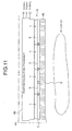
- the group of photomultiplier tubes G has the photomultiplier tubes 1 arranged in a matrix, as described above. As shown in Fig. 12, the group of photomultiplier tubes G includes a photomultiplier tube unit S having four 2 x 2 of the photomultiplier tubes 1. The arrangement of the photomultiplier tubes 1 in the unit S is one example.
- the photomultiplier tubes 1 having the same structure are arranged in a 2 x 2 matrix.
- the neighboring side surfaces 3c of the four faceplates 3 are in close contact, while neighboring side tubes 2 are separated from one another. Neighboring faceplates 3 can be easily and reliably fixed together by adhesive.
- the stem plate 4 of each photomultiplier tube 1 in the 2 x 2 photomultiplier tube unit S has a cylindrical spacer 31, as one example of the threaded portions 30.
- the photomultiplier tubes 1 are arranged on an upper surface of a single first circuit board 50.
- the first circuit board 50 may include a voltage dividing circuit (bleeder circuit) which is connectable to each of the dynode pins 10A, or a circuit pattern which is connectable to each of the anode pins 10B for extracting anode output.
- the first circuit board 50 is also provided with metal socket pins 51 corresponding to anode pins 10B and metal socket pins 52 corresponding to dynode pins 10A.
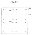
- a single second circuit board 55 is provided under the first circuit board 50 and parallel thereto.
- the second circuit board 55 is electrically connected to the first circuit board 50 through connecting pins (not shown).
- the second circuit board 55 has a function for calculating a position, such as an AD converter.
- Spacers 56 that are electrically isolated and cylindrical in shape protrude from the top surface of the second circuit board 55 at positions corresponding to screw insertion holes 53 formed in the first circuit board 50.
- the spacers 56 maintain a predetermined interval between the first circuit board 50 and the second circuit board 55. Screw insertion holes 56a are formed in the spacers 56.
- this structure simplifies the assembly of the first circuit board 50, the second circuit board 55, and the photomultiplier tube 1, thereby reducing the assembly time and reducing the cost of the product.
- the first circuit board 50, the second circuit board 55, and the photomultiplier tube 1 can be easily separated, thereby facilitating the operation of replacing parts. Additionally, discarding the entire unit may be avoided.
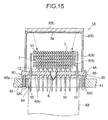
- FIG. 15 shows another type of photomultiplier tube 1A having a stem plate 4A with screw portions 60.
- the screw portions 60 have annular spacers 65 in order to improve mountability.
- Female threads 65a are formed at predetermined positions on the bottom surface of the spacers 65.
- the photomultiplier tube 1A is fixed to a base 61 of a common photodetector.
- screw insertion holes 62 are formed in the base 61 at positions corresponding to the screw portions 60.
- Socket openings 64 are formed in the base 61 for inserting a socket 63 into the stem pins 10.
- Screws 32C male screws
- the circuit boards 33, 37, 50, and 55 are configured to have components required for the photomultiplier tube 1.
- the components may be changed appropriately depending on the application thereof.
- the circuit boards 33 and 50 described above can also be formed of plastic or ceramics in a flat shape on which no circuit is mounted.
- a photomultiplier tube, a photomultiplier tube unit, and a radiation detector according to the present invention have a lot of different applications in imaging devices for a low luminescent object, such as gamma cameras.
Landscapes
- Measurement Of Radiation (AREA)
- Nuclear Medicine (AREA)
Abstract
Description
Claims (12)
- A photomultiplier tube (1) comprising: a photocathode (3a) for emitting electrons in response to light incident on a faceplate (3); an electron multiplier (9) provided in an hermetically sealed vessel (5) for multiplying electrons emitted from the photocathode (3a); and an anode (12) for generating an output signal based on electrons multiplied by the electron multiplier, characterized in that the hermetically sealed vessel (5) includes:a stem plate (4) having stem pins (10) for fixing the electron multiplier (9) and the anode (12) thereon;a metal side tube (2) enclosing the electron multiplier (9) and the anode (12), the metal side tube having an open end (B) to which the stem plate (4) is fixed; andthe faceplate (3) fixed to another open end (A) of the side tube (2), the faceplate (3) being made from glass, screw means (30) being provided at a lower surface of the stem plate (4).
- The photomultiplier tube according to claim 1, characterized in that the screw means (30) includes a spacer (31) projecting from the lower surface of the stem plate (4), the spacer having a female thread (31a) in the interior thereof.
- The photomultiplier tube according to claim 1 or 2, characterized in that the photomultiplier tube further comprises:a circuit board (33) extending parallel to the stem plate (4) and electrically connected to the stem pins (10), the circuit board (33) being secured to the stem plate (4) by screwing a male screw member (32) into the screw means (30).
- The photomultiplier tube according to claim 1 or 2, characterized in that the photomultiplier tube further comprises a first circuit board (33) detachable with the stem plate (4), the first circuit board (33) being secured to the stem plate (4) by screwing a screw member (32) into the screw means (30) through the first circuit board (33).
- The photomultiplier tube according to claim 4, characterized in that the screw means (30) includes a spacer (31) projecting from the lower surface of the stem plate (4), the spacer (31) being integral with the stem plate (4) from the same material as the stem plate (4), the spacer (31) spacing the first circuit board (33) away from the stem plate (4).
- The photomultiplier tube according to claim 4, characterized in that the screw member (32) is made from an electrically insulating material.
- The photomultiplier tube according to claim 4, characterized in that the screw means (30) includes a spacer (31) projecting from the lower surface of the stem plate (4), the spacer (31) being made from an electrically insulating material, the spacer (31) spacing the first circuit board (33) away from the stem plate (4).
- The photomultiplier tube according to claim 4, characterized in that the screw member (32) is made from an electrically insulating material.
- The photomultiplier tube according to claim 1 or 2, characterized in that the photomultiplier tube comprises a second circuit board (37) detachable with the stem plate (4) and the first circuit board (33), the first and second circuit boards (33, 37) being secured to the stem plate (4) by screwing the screw member (32) into the screw means (30) through the first and second circuit boards (33, 37).
- A photomultiplier tube unit comprising a plurality of photomultiplier tubes (1) that are juxtaposed, each of the plurality of the photomultiplier tubes (1) having a photocathode (3a) for emitting electrons in response to light incident on a faceplate (3); an electron multiplier (9) provided in an hermetically sealed vessel (5) for multiplying electrons emitted from the photocathode (3a); and an anode for generating an output signal based on electrons multiplied by the electron multiplier (9), characterized in that the hermetically sealed vessel (5) includes:a stem plate (4) having stem pins (10) for fixing the electron multiplier (9) and the anode (12) thereon;a metal side tube (2) enclosing the electron multiplier (9) and the anode (12), the side tube (2) having one open end (B) to which the stem plate (4) is fixed; andthe faceplate (3) fixed to another open end (A) of the side tube (2), the faceplate being made from glass, and that screw means (30) is provided on a lower surface of the stem plate (4), the hermetically sealed vessels (5) are secured on a single substrate by screwing male screw members (32A, 32b) into the screw means (30) while the hermetically sealed vessels (5) are juxtaposed on the substrate.
- The photomultiplier tube unit according to claim 10, characterized in that the substrate is a circuit board (50) electrically connectable to the stem pins (10), and the male screw members (32A, 32b) are electrically insulating screws.
- A radiation detector comprising a scintillator (46) for emitting fluorescent light in response to radiation generated from an object (P); a plurality of photomultiplier tubes (1) arranged in a manner that faceplates (3) of the photomultiplier tubes (1) face the scintillator (46), each of the photomultiplier tubes (1) generating an electrical charge based on the fluorescent light emitted from the scintillator (46); and a position calculating processor (49) for processing an output from the photomultiplier tube (1) and generating a signal for indicating a position of radiation generated in the object (P), characterized in that each of the plurality of photomultiplier tubes (1) has a photocathode (3a) for emitting electrons in response to light incident on a faceplate (3); an electron multiplier (9) provided in an hermetically sealed vessel (5) for multiplying electrons emitted from the photocathode (3a); and an anode for producing an output signal based on electrons multiplied by the electron multiplier (9), the hermetically sealed vessel (5) includes:a stem plate (4) having stem pins (10) for securing the electron multiplier (9) and the anode (12) thereon;a metal side tube (2) enclosing the electron multiplier (9) and the anode (12), the side tube having one open end (B) to which the stem plate (4) is fixed; andthe faceplate (3) fixed to another open end (A) of the side tube (2), the faceplate being made from glass, screw means (30) is provided at a lower surface of the stem plate (4), and the hermetically sealed vessels (5) are arranged and secured to a signel substrate by screwing male screw members (32A, 32B) into the screw means (30) while the hermetically sealed vessels (5) are juxtaposed on the substrate.
Applications Claiming Priority (2)
| Application Number | Priority Date | Filing Date | Title |
|---|---|---|---|
| JP31920898A JP3919363B2 (en) | 1998-11-10 | 1998-11-10 | Photomultiplier tube, photomultiplier tube unit and radiation detector |
| PCT/JP2000/002929 WO2001086692A1 (en) | 1998-11-10 | 2000-05-08 | Photomultiplier tube, photomultiplier tube unit, radiation detector |
Publications (3)
| Publication Number | Publication Date |
|---|---|
| EP1304720A1 true EP1304720A1 (en) | 2003-04-23 |
| EP1304720A4 EP1304720A4 (en) | 2007-02-28 |
| EP1304720B1 EP1304720B1 (en) | 2009-08-26 |
Family
ID=26344898
Family Applications (1)
| Application Number | Title | Priority Date | Filing Date |
|---|---|---|---|
| EP00922982A Expired - Lifetime EP1304720B1 (en) | 1998-11-10 | 2000-05-08 | Photomultiplier tube, photomultiplier tube unit, radiation detector |
Country Status (3)
| Country | Link |
|---|---|
| EP (1) | EP1304720B1 (en) |
| JP (1) | JP3919363B2 (en) |
| WO (1) | WO2001086692A1 (en) |
Cited By (4)
| Publication number | Priority date | Publication date | Assignee | Title |
|---|---|---|---|---|
| EP1304719A4 (en) * | 1998-11-10 | 2007-02-14 | Hamamatsu Photonics Kk | Photomultiplier tube, photomultiplier tube unit, and radiation detector |
| EP1304718A4 (en) * | 1998-11-10 | 2007-02-14 | Hamamatsu Photonics Kk | Photomultiplier tube and production method therefor |
| EP1282150A4 (en) * | 1998-11-10 | 2007-02-28 | Hamamatsu Photonics Kk | Photomultiplier tube |
| US7276704B1 (en) | 2000-05-08 | 2007-10-02 | Hamamatsu Photonics K.K. | Photomultiplier tube, photomultiplier tube unit, and radiation detector |
Families Citing this family (10)
| Publication number | Priority date | Publication date | Assignee | Title |
|---|---|---|---|---|
| US6852979B1 (en) | 1998-11-10 | 2005-02-08 | Hamamatsu Photonics K. K. | Photomultiplier tube, photomultiplier tube unit, radiation detector |
| JP3919363B2 (en) * | 1998-11-10 | 2007-05-23 | 浜松ホトニクス株式会社 | Photomultiplier tube, photomultiplier tube unit and radiation detector |
| US6794629B2 (en) | 2001-02-23 | 2004-09-21 | Hamamatsu Photonics K.K. | Photomultiplier |
| JP4421209B2 (en) * | 2003-04-11 | 2010-02-24 | 浜松ホトニクス株式会社 | Radiation detector |
| US7141926B2 (en) * | 2004-08-10 | 2006-11-28 | Burle Technologies, Inc. | Photomultiplier tube with improved light collection |
| JP4744844B2 (en) * | 2004-10-29 | 2011-08-10 | 浜松ホトニクス株式会社 | Photomultiplier tube and radiation detector |
| JP4649583B2 (en) * | 2006-06-27 | 2011-03-09 | 大学共同利用機関法人 高エネルギー加速器研究機構 | Neutron incident position detector |
| JP5856830B2 (en) * | 2011-12-13 | 2016-02-10 | 浜松ホトニクス株式会社 | Optical measuring device |
| KR101705425B1 (en) * | 2015-01-22 | 2017-02-09 | 서준석 | SMT-packaged SiPM sensor |
| CN121165152A (en) * | 2025-07-31 | 2025-12-19 | 中国原子能科学研究院 | Photomultiplier tube and nuclear radiation detector testing device and method |
Family Cites Families (3)
| Publication number | Priority date | Publication date | Assignee | Title |
|---|---|---|---|---|
| JP3215486B2 (en) * | 1992-04-09 | 2001-10-09 | 浜松ホトニクス株式会社 | Photomultiplier tube |
| JP4231120B2 (en) * | 1998-06-01 | 2009-02-25 | 浜松ホトニクス株式会社 | Photomultiplier tube and radiation detector |
| JP3919363B2 (en) * | 1998-11-10 | 2007-05-23 | 浜松ホトニクス株式会社 | Photomultiplier tube, photomultiplier tube unit and radiation detector |
-
1998
- 1998-11-10 JP JP31920898A patent/JP3919363B2/en not_active Expired - Fee Related
-
2000
- 2000-05-08 WO PCT/JP2000/002929 patent/WO2001086692A1/en not_active Ceased
- 2000-05-08 EP EP00922982A patent/EP1304720B1/en not_active Expired - Lifetime
Cited By (5)
| Publication number | Priority date | Publication date | Assignee | Title |
|---|---|---|---|---|
| EP1304719A4 (en) * | 1998-11-10 | 2007-02-14 | Hamamatsu Photonics Kk | Photomultiplier tube, photomultiplier tube unit, and radiation detector |
| EP1304718A4 (en) * | 1998-11-10 | 2007-02-14 | Hamamatsu Photonics Kk | Photomultiplier tube and production method therefor |
| EP1282150A4 (en) * | 1998-11-10 | 2007-02-28 | Hamamatsu Photonics Kk | Photomultiplier tube |
| US7276704B1 (en) | 2000-05-08 | 2007-10-02 | Hamamatsu Photonics K.K. | Photomultiplier tube, photomultiplier tube unit, and radiation detector |
| US7495223B2 (en) | 2000-05-08 | 2009-02-24 | Hamamatsu Photonics K. K. | Photomultiplier tube, photomultiplier tube unit, and radiation detector |
Also Published As
| Publication number | Publication date |
|---|---|
| JP2000149863A (en) | 2000-05-30 |
| WO2001086692A1 (en) | 2001-11-15 |
| EP1304720A4 (en) | 2007-02-28 |
| EP1304720B1 (en) | 2009-08-26 |
| JP3919363B2 (en) | 2007-05-23 |
Similar Documents
| Publication | Publication Date | Title |
|---|---|---|
| EP1304720B1 (en) | Photomultiplier tube, photomultiplier tube unit, radiation detector | |
| US6472664B1 (en) | Photomultiplier tube tightly arranged with substantially no space between adjacent tubes | |
| US6265812B1 (en) | Electron multiplier | |
| US7495223B2 (en) | Photomultiplier tube, photomultiplier tube unit, and radiation detector | |
| US6650049B1 (en) | Photomultiplier tube | |
| US7812532B2 (en) | Photomultiplier tube, radiation detecting device, and photomultiplier tube manufacturing method | |
| US6946641B1 (en) | Photomultiplier tube | |
| US7847232B2 (en) | Photomultiplier tube and radiation detecting device employing the photomultiplier tube | |
| US7902509B2 (en) | Photomultiplier tube and radiation detecting device | |
| US6852979B1 (en) | Photomultiplier tube, photomultiplier tube unit, radiation detector | |
| US7838810B2 (en) | Photomultiplier tube and a radiation detecting device employing the photomultiplier tube | |
| JP4231120B2 (en) | Photomultiplier tube and radiation detector | |
| EP1304719A1 (en) | Photomultiplier tube, photomultiplier tube unit, and radiation detector | |
| JP2000067801A (en) | Photomultiplier tube unit and radiation detector | |
| JP4231121B2 (en) | Photomultiplier tube and radiation detector | |
| CN1452779A (en) | Photomultiplier tube, photomultiplier tube unit and radiation detector |
Legal Events
| Date | Code | Title | Description |
|---|---|---|---|
| PUAI | Public reference made under article 153(3) epc to a published international application that has entered the european phase |
Free format text: ORIGINAL CODE: 0009012 |
|
| 17P | Request for examination filed |
Effective date: 20021128 |
|
| AK | Designated contracting states |
Designated state(s): AT BE CH CY DE DK ES FI FR GB GR IE IT LI LU MC NL PT SE |
|
| AX | Request for extension of the european patent |
Extension state: AL LT LV MK RO SI |
|
| RBV | Designated contracting states (corrected) |
Designated state(s): AT BE CH DE FR GB LI |
|
| A4 | Supplementary search report drawn up and despatched |
Effective date: 20070129 |
|
| RIC1 | Information provided on ipc code assigned before grant |
Ipc: H01J 43/04 20060101AFI20070123BHEP |
|
| GRAP | Despatch of communication of intention to grant a patent |
Free format text: ORIGINAL CODE: EPIDOSNIGR1 |
|
| GRAS | Grant fee paid |
Free format text: ORIGINAL CODE: EPIDOSNIGR3 |
|
| GRAA | (expected) grant |
Free format text: ORIGINAL CODE: 0009210 |
|
| AK | Designated contracting states |
Kind code of ref document: B1 Designated state(s): DE FR GB |
|
| REG | Reference to a national code |
Ref country code: GB Ref legal event code: FG4D |
|
| REF | Corresponds to: |
Ref document number: 60042848 Country of ref document: DE Date of ref document: 20091008 Kind code of ref document: P |
|
| PLBE | No opposition filed within time limit |
Free format text: ORIGINAL CODE: 0009261 |
|
| STAA | Information on the status of an ep patent application or granted ep patent |
Free format text: STATUS: NO OPPOSITION FILED WITHIN TIME LIMIT |
|
| 26N | No opposition filed |
Effective date: 20100527 |
|
| PGFP | Annual fee paid to national office [announced via postgrant information from national office to epo] |
Ref country code: DE Payment date: 20120502 Year of fee payment: 13 |
|
| PGFP | Annual fee paid to national office [announced via postgrant information from national office to epo] |
Ref country code: GB Payment date: 20120502 Year of fee payment: 13 Ref country code: FR Payment date: 20120608 Year of fee payment: 13 |
|
| GBPC | Gb: european patent ceased through non-payment of renewal fee |
Effective date: 20130508 |
|
| PG25 | Lapsed in a contracting state [announced via postgrant information from national office to epo] |
Ref country code: DE Free format text: LAPSE BECAUSE OF NON-PAYMENT OF DUE FEES Effective date: 20131203 |
|
| REG | Reference to a national code |
Ref country code: DE Ref legal event code: R119 Ref document number: 60042848 Country of ref document: DE Effective date: 20131203 |
|
| REG | Reference to a national code |
Ref country code: FR Ref legal event code: ST Effective date: 20140131 |
|
| PG25 | Lapsed in a contracting state [announced via postgrant information from national office to epo] |
Ref country code: GB Free format text: LAPSE BECAUSE OF NON-PAYMENT OF DUE FEES Effective date: 20130508 |
|
| PG25 | Lapsed in a contracting state [announced via postgrant information from national office to epo] |
Ref country code: FR Free format text: LAPSE BECAUSE OF NON-PAYMENT OF DUE FEES Effective date: 20130531 |