EP1301964B1 - System for increasing antenna efficiency - Google Patents
System for increasing antenna efficiency Download PDFInfo
- Publication number
- EP1301964B1 EP1301964B1 EP01948841A EP01948841A EP1301964B1 EP 1301964 B1 EP1301964 B1 EP 1301964B1 EP 01948841 A EP01948841 A EP 01948841A EP 01948841 A EP01948841 A EP 01948841A EP 1301964 B1 EP1301964 B1 EP 1301964B1
- Authority
- EP
- European Patent Office
- Prior art keywords
- communications device
- electrical connection
- section
- conductive
- point
- Prior art date
- Legal status (The legal status is an assumption and is not a legal conclusion. Google has not performed a legal analysis and makes no representation as to the accuracy of the status listed.)
- Expired - Lifetime
Links
Images


Classifications
-
- H—ELECTRICITY
- H01—ELECTRIC ELEMENTS
- H01Q—ANTENNAS, i.e. RADIO AERIALS
- H01Q1/00—Details of, or arrangements associated with, antennas
- H01Q1/48—Earthing means; Earth screens; Counterpoises
-
- H—ELECTRICITY
- H01—ELECTRIC ELEMENTS
- H01Q—ANTENNAS, i.e. RADIO AERIALS
- H01Q1/00—Details of, or arrangements associated with, antennas
- H01Q1/12—Supports; Mounting means
- H01Q1/22—Supports; Mounting means by structural association with other equipment or articles
- H01Q1/24—Supports; Mounting means by structural association with other equipment or articles with receiving set
- H01Q1/241—Supports; Mounting means by structural association with other equipment or articles with receiving set used in mobile communications, e.g. GSM
- H01Q1/242—Supports; Mounting means by structural association with other equipment or articles with receiving set used in mobile communications, e.g. GSM specially adapted for hand-held use
- H01Q1/243—Supports; Mounting means by structural association with other equipment or articles with receiving set used in mobile communications, e.g. GSM specially adapted for hand-held use with built-in antennas
Definitions
- the present invention is directed toward a communications device, and more particularly toward increasing efficiency of an antenna for a communications device.
- a communications device typically includes a front section and a rear section, the front and rear sections acting as a housing for a circuit board.
- the circuit board includes the control circuitry for the cellular telephone.
- the cellular telephone further includes an antenna coupled to the circuit board used for transmitting and receiving information to and from a cellular base station.
- Cellular telephones are usually powered by a battery, the negative terminal of which is the lowest point of potential for the cellular telephone. When transmitting information from the cellular telephone to the cellular base station, battery power is consumed and therefore the operational availability of the device is shortened.
- one or both ofthe front and rear sections have in some cases been conductive, that is made of or coated with a conductive material. Where one or both of the sections are conductive, the conductive sections have sometimes been unconnected from the point. of lowest potential, and in other cases have been connected to the point of lowest potential via a circuit board trace located around an entire perimeter of the circuit board. When the section(s) are conductive and connected to the point of lowest potential by the perimeter trace, the conductive sections serve as a ground plane for the antenna, aiding in the transmission and reception of information from and to the cellular telephone.
- EP 0 522 532 A2 discloses such a communication device according to the preamble of claim 1.
- antenna efficiency is not optimized. A less efficient cellular telephone antenna causes more battery power to be consumed when transmitting information to the cellular base station. Because battery power is limited, it is desirable to increase the efficiency of the antenna.
- the present invention is directed to overcoming the problem discussed above.
- a communications device is provided as defined in claim 1.
- the electrical connection is located other than along the perimeter of the circuit board, and may comprise a plurality of contact locations.
- the electrical connection may be a capacitor or an inductor.
- the electrical connection may also have a major dimension of length less than one-tenth P.
- the communications device includes a negative power terminal, and the point of lowest potential is an electrical connection with the negative power terminal.
- the electrical connection from the one section and the point of lowest potential is proximate to the negative power terminal.
- the one section may be metalized or may be formed from metal.
- the communications device further comprises a second electrical connection between the other section and the point of lowest potential, where the second electrical connection has a length less than one-half P.
- the other of the front section and the rear section is conductive, and the communications device further comprises a second electrical connection between the other section and the point of lowest potential substantially along the entire perimeter of the circuit board.
- the other of the front section and the rear section is conductive and electrically unconnected from the point of lowest potential.
- a communications device is provided as defined in claim 15.
- the electrical connection may comprise a plurality of contact locations, and may be formed by a capacitor or an inductor.
- the electrical connection further may have a major dimension less than one-tenth P.
- a second electrical connection is located between the other section and the circuit board ground plane, where the second electrical connection has a major dimension less than 1 ⁇ 2P.
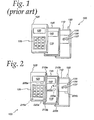
- Fig. 1 illustrates the electrical connection between a printed circuit board (PCB) and a housing of a mobile terminal such as a cellular telephone 100 in accordance with the prior art.
- the cellular telephone 100 includes the housing designated by a front section 105 and a rear section 110, and a PCB 115.
- the front section 105 includes an LCD lens 120 and a keypad 125.
- An antenna 130 is mounted to the rear section 110 for receiving and transmitting information to and from a cellular base station (not shown).
- a battery 135 with positive and negative power terminals 136, 137 respectively is also mounted to the rear section 110.
- the PCB 115 is connected to the power terminals 136, 137 and to the antenna 130.
- An LCD 140 is mounted on the PCB 115, such that when the cellular telephone 100 is assembled, the LCD 140 is viewable through the LCD lens 120.
- the PCB further includes a PCB trace 145 located along an entire perimeter P of the PCB 115, where the PCB trace 145 is connected to a cellular telephone point of lowest potential. Typically, the point of lowest potential is the negative power terminal 137.
- the PCB trace 145 may also be exposed on a back side of the PCB 115.
- the conductive section(s) have sometimes been unconnected from the point of lowest potential, and in other cases have been connected to the point of lowest potential along the entire perimeter P of the PCB 115 via the PCB trace 145.
- the electrical connections are typically made using a conductive caulk, a conductive elastomer, or a conductive gasket along a perimeter of the respective front and rear section.
- Fig. 2 illustrates a communications device embodying the present invention.
- Components of Fig. 2 identified by reference numerals identical to those of Fig. 1 are the same and will not be discussed in detail.
- the front section 105 is conductive, that is formed from metal, formed from a conductive material such as a conductive plastic, or coated with a conductive material along an inner surface of the front section 105.
- the front section 105 is unconnected from the point of lowest potential, for example the negative battery terminal 137 or some terminal connected thereto, except for an electrical connection between positions designated as 205a and 205b, where 205b is further connected to the point of lowest potential 137.
- the front section 105 is unconnected from the point of lowest potential 13 7 except for an electrical connection between an entire side 210a of the front section 105 designated by area 210a and a side of the PCB 115 along, for example, the portion of the PCB trace 145 designated within the area 21 0b.
- the front section 105 is conductive
- the front section 105 is unconnected from the point oflowest potential 137 except for two (2) electrical connections coupling the front section 105 to the point of lowest potential 137.
- electrical connections extending between positions 215a and 215b and positions 220a and 220b electrically couple the front section 105 to the point of lowest potential 13 7, where the electrical connections 215b and 220b are connected to the point of lowest potential 137.
- the rear section 110 is conductive, and is unconnected from the point of lowest potential except for an electrical connection between a position 225a located on a back of the PCB 115, and a position 225b, where the position 225a is connected to the point of lowest potential 137.
- both the front and rear sections 105 and 110 are conductive and one of the front and rear sections is connected to the point of lowest potential 137 with the electrical connection having a major dimension less than 1 ⁇ 2P.
- the other of the front and rear sections is coupled to the point of lowest potential by a second electrical connection having a major dimension less then 1 ⁇ 2P, or via an electrical connection around the entire perimeter P of the circuit board via the PCB trace 145.
- the electrical connection from the respective conductive section to the point of lowest potential increases the antenna efficiency of the antenna 130.
- Increasing antenna efficiency allows the cellular telephone to transmit a signal having the same strength as a cellular telephone utilizing prior art electrical connection techniques between the conductive section(s) and the point of lowest potential, while consuming less battery power.
- the electrical connections utilized in the embodiment just described allow a greater signal strength to be transmitted from the cellular telephone over that of the prior art, while consuming the same battery power as the cellular telephone utilizing prior art electrical connections between the conductive section(s) and the point of lowest potential.
- the electrical connections may be formed using wire, conductive foam, conductive elastomer, conductive gasket material, or any other material sufficient for forming an adequate electrical ground.
- the size of the electrical connection is not vital so long as it is sufficient (large enough) to form an adequate ground, and has a major dimension less than one-halfP.
- a minimum size for an electrical connection to form an adequate electrical ground is known to one skilled in the art.
- a typical thickness for the electrical connection ranges from a width of a wire, or conductive sheet of approximately 1 mm width, to a width of a circular bead of conductive material (for example conductive foam or gasket) of approximately 6 mm diameter.
- the width ofthe electrical connection may be less so long as an adequate electrical ground is formed, and the width may be greater where placement of components in the communications device or other manufacturing considerations allow.
- the height of the electrical connection is typically that of a distance between the respective positions between which the electrical connection is made when the front section 105, the rear section 110 and the PCB 115 are assembled together.
- the height of the electrical connection may be greater, especially for example, where the electrical connection is formed from a compressible material such as a conductive foam or gasket, or from a conductive material having spring-like properties.
- the electrical connection may be formed using an inductor or a capacitor, further discussed below.
- the position for the electrical connection between the respective conductive section and the point of lowest potential it is preferable to select a position proximate the negative battery terminal 137.
- the preferred position may not always be achieved. For example, ifit is desired to connect a conductive front section 105 to the point of lowest potential, and the negative battery terminal 137 is positioned directly beneath the LCD 140 and the LCD lens 120, a connection between the front section 105 and the PCB 115 could not be achieved directly above the negative battery terminal 137. In such situations, the position of the electrical connection is selected such that the point of contact between the front section 105 and the PCB 115 are close to but not directly above the negative battery terminal 137.
- the electrical connection be proximate the negative battery terminal, improved antenna performance is also achieved where the electrical connection is not proximate the negative battery terminal.
- Figs. 3a and 3b are exploded side and side by side section views, respectively, of an Ericsson cellular telephone 300, model #A1228d, in accordance with an embodiment of the present invention.
- a front section 305, a rear section 310, and a PCB 315 are shown.
- the PCB 315 includes a PCB trace 317 exposed on a front and a back of the PCB 315 along the perimeter of the PCB.
- the PCB trace 317 is connected to a PCB ground plane 318 which is connected to the point of lowest potential for the cellular telephone, typically a negative power terminal 319 of a battery 320.
- the PCB 315 further includes a shield can 321 which is connected to the PCB ground plane 318.
- the shield can is conductive, and is typically used for electrostatic discharge protection, and/or to reduce emissions from the cellular telephone.
- the PCB is connected to an antenna 322, used for receiving and transmitting information to and from the cellular telephone.
- Both the front and rear section 305 and 310 are metalized, that is coated with a conductive material.
- the rear section 310 is connected to the PCB ground plane around an entire perimeter P of the PCB 315 via the PCB trace 317.
- the front section 305 is isolated from the PCB ground plane except for an electrical connection 335 which extends between a position 340a on the front section 305, and a position 340b located on the shield can 321.
- Positions 340a and 340b are located approximately 21 mm from a top of the cellular telephone 300, designated generally by arrow 350, and approximately 11 mm from a left side of the cellular telephone 300, designated generally by an arrow 355.
- the electrical connection 335 is formed from a conductive elastomer having a substantially circular configuration of approximately 3 mm diameter. The elastomer is of sufficient height such that when the PCB 315 is assembled within the front section 305, the electrical connection 335 contacts both the front section 305 and the shield can 320. Electrically connecting the front section 305 to the point of lowest potential in this manner improves antenna efficiency of the antenna 322 by approximately 65%.
- Figs. 4a and 4b are exploded side and side by side views, respectively, of an Ericsson cellular telephone 400, model #T28s, in accordance with another embodiment of the present invention.
- a front section 405, a rear section 410, and a PCB 415 are shown.
- the PCB 415 includes a PCB trace 417 exposed on a front and a back of the PCB 415 along the perimeter of the PCB.
- the PCB trace 417 is connected to a PCB ground plane 418 which is connected to the point of lowest potential for the cellular telephone, typically a negative power terminal 419 of a battery 420.
- the PCB 415 is electrically connected to an antenna 422.
- Both the front and rear sections 405 and 410 are conductive, where the front section 405 is metalized, and the rear section 410 is made of metal.
- the rear section 410 is connected to the PCB ground plane 418 around the entire perimeter P of the PCB 415 via the PCB trace 417.
- the front section 405 is isolated from the PCB ground plane except for an electrical connection 435 which extends between a position 440a on the front section 405, and a position 440b located on the PCB 415.
- the positions 440a and 440b are located approximately 20 mm from a top of the cellular telephone 400 designated generally by an arrow 450, and approximately 24 mm from a right side of the cellular telephone designated generally by an arrow 457.
- the electrical connection 435 is formed from an inductor.
- the inductor may have from 2 to 6 turns, such as 3.5 to 4 turns.
- the inductor has an air core with a diameter of approximately 4 mm. Electrically connecting the front section 405 to the point of lowest potential 419 in this manner improves antenna efficiency of the antenna 422 by approximately 65%.
- Figs. 5a and 5b are exploded side and side by side views, respectively, of an Ericsson cellular telephone 500, model #KH668, in accordance with an embodiment ofthe present invention.
- a front section 505, a rear section 510, and a PCB 515 are shown.
- the PCB 515 includes a PCB trace 517 exposed on a front and a back of the PCB 515 along a perimeter of the PCB.
- the PCB trace 517 is connected to a PCB ground plane 518 which is coupled to the point of lowest potential for the cellular telephone 500, typically a negative power terminal 519 of a battery 520.
- the PCB 515 is electrically connected to an antenna 522.
- the front section 505 is metalized, and the rear section 510 is made of metal.
- the rear section 510 is connected to the PCB point of lowest potential around the entire perimeter P of the PCB 515 via PCB trace 517.
- the front section 505 is isolated from the PCB point of lowest potential except for two electrical connections 535 and 537.
- One electrical connection 535 extends between a position 535a located on the front section 505 and a position 535b which is located on the front of the PCB 515.
- the other electrical connection 537 extends between a position 537a located on the front section 505 and a. position 537b located on the front of the PCB 515.
- the positions 535b and 537b are coupled to the point of lowest potential for the cellular telephone 500, for example, via the PCB trace 517.
- Positions 535a and 535b are located approximately 6 mm from a left side of the cellular telephone 500 designated generally by an arrow 555, and approximately 6 mm from a bottom of the cellular telephone designated generally by an arrow 559.
- Positions 537a and 537b are located approximately 6 mm from a right side of the cellular telephone 500 designated generally by an arrow 557, and approximately 6 mm from the bottom designated at 559.
- the electrical connections 535 and 537 are formed from respective screw bosses approximately 5 mm in diameter, which electrically connect the front section 505 to the PCB 515 when the front section and the PCB are assembled. Electrically connecting the front section 505 to the point of lowest potential 519 in this manner improves antenna efficiency of the antenna 522 by approximately 20%.
- a conductive section is connected to the point of lowest potential via an electrical connection having a length less than one-half the perimeter of the PCB, or is completely unconnected from the point of lowest potential.
- a portion around a perimeter of the front section 505, designated in the area 570, is not metalized with the rest of the front section 505, to ensure that when the PCB 515 is assembled with the front section 505, the front section 505 is not connected to the point oflowest potential along the entire perimeter of the front section 505 via the PCB trace 517.
- the entire front section 505 may be metalized, with an insulating material placed around the perimeter of the front section 505 to ensure that the front section 505 does not contact the point of lowest potential around the entire perimeter of the front section via the PCB trace 517.
- Figs. 6a and 6b are exploded side and side by side views, respectively, of an Ericsson cellular telephone 600, model #A2218d, in accordance with another embodiment of the present invention.
- a front section 605, a rear section 610, and a PCB 615 are shown.
- the PCB 615 includes a PCB trace 617 exposed on a front and a back of the PCB 615 extending along a perimeter of the PCB.
- the PCB trace 617 is connected to a PCB ground plane 618 which is coupled to a point of lowest potential for the cellular telephone 600, typically a negative power terminal 619 of a battery 620.
- a shield can 621 is formed from metalized plastic and is coupled to the back of the PCB 615 via the PCB trace 617.
- the PCB 615 is further coupled to an antenna 622.
- the front section 605 is metalized, and the rear section 610 is made of plastic.
- the shield can 621 is connected to the point of lowest potential around the entire perimeter P of the PCB 615 via the PCB trace 617.
- the front section 605 is unconnected from the point of lowest potential except for an electrical connection 63 5 which extends between a position 635a on the front section 605, and a position 635b located on the front and side of the PCB 615.
- the electrical connection 635 and the corresponding position 635a and 635b are located along a left side of the cellular telephone 600, generally designated by an arrow 655, approximately 77 mm from a top of the cellular telephone, generally designated by an arrow 650.
- the electrical connection 635 is formed from a conductive elastomer of approximately 4 mm width and 5 mm length, such that when the front section 605 and the PCB 615 are assembled, the front section 605 is coupled to the point of lowest potential. Electrically connecting the front section 605 to the point oflowest potential 625 in this manner improves antenna efficiency by approximately 50%.
- the electrical connection 635 and respective positions 635a and 635b are located on a right side of the cellular telephone 600 approximately 77 mm from the top 650.
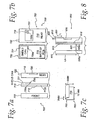
- Figs. 7a and 7b are exploded side and side by side views, respectively, of an Ericsson cellular telephone 700, model #KF788, according to another embodiment ofthe present invention.
- a front section 705, a rear section 710 and a PCB 715 are shown.
- the PCB 715 includes a PCB ground plane 718 which is connected to the point of lowest potential for the cellular telephone 700, typically a negative power terminal 719 of a battery 720.
- the PCB 715 further includes a shield can 721 which is coupled to the PCB ground plane.
- the PCB 715 is electrically connected to an antenna 722. Both the front and rear sections 705 and 710 are metalized.
- the front section 705 is isolated from the point of lowest potential.
- the rear section 710 is isolated from the point of lowest potential except for an electrical connection 735 extending between a position 735a located on the shield can 721, and a position 735b located on the rear section 710.
- the positions 735a and 735b are located approximately 41 mm from a top of the cellular telephone 700 designated generally by an arrow 750, and approximately 1 mm from a right side of the cellular telephone 700 designated generally by an arrow 757.
- Figure 7c further illustrates the electrical connection 735, which may be formed from a sheet of metal bent in a "J" configuration.
- the electrical connection 735 has a height of approximately 5 mm, a length of approximately 12 mm, and a curved portion designated generally at 760 having a diameter of approximately 2 mm.
- the length of the electrical connection 735 may be approximately I cm.
- a bottom portion 760 of the electrical connection 735 is installed in a battery clip for the negative power terminal 719 and makes contact with metalized rear housing 710, and a top portion of the electrical connector 73 designated at the curved section 765 makes contact with the shield can 721. Electrically connecting the rear section 710 to the point of lowest potential in this manner improves antenna efficiency by approximately 40%.
- the electrical connection between the front section and the PCB causes a quarter wave, wave guide trap to be formed between the front section and the PCB, as described with respect to Figs. 8-10.
- Figs. 8-10 are exploded side views of a cellular telephone in accordance with embodiments of the present invention.
- Figs. 8-10 show a front section 805, a rear section 810, and a PCB 815.
- the PCB 815 includes a ground plane 818 which is connected to the cellular telephone 800 point of lowest potential, typically a negative power terminal (not shown) of a battery 820.
- the PCB further includes a PCB trace (not shown) exposed on a front and a back of the PCB, similar to the PCB traces of Figs. 3b, 4b, 5b and 6b extending around a complete perimeter of the PCB, and connected to the PCB ground plane 818.
- the rear section 810 is connected to the PCB 815 around the entire perimeter P of the PCB 815 via the PCB trace.
- An antenna 822 is coupled to the PCB 815 used for receiving and transmitting information to/from the cellular telephone.
- an electrical connection 825 is formed between position 825a on the front section 805 and position 825b located on the PCB 815. Position 825b is further coupled to the PCB ground plane 818.
- the electrical connection is positioned approximately ⁇ /4 from a top of the front section 805 and PCB 815 such that a quarter wave, wave guide trap is formed between the front section and the PCB 815, with a low current point (or high impedance Z) near the antenna 822. This presents a very high impedance to the normal current path down the front of the telephone, causing the ground currents i t to flow down the rear section 810 of the cellular telephone as designated by an arrow 830.
- the ground currents i t are not restricted from flowing down the sides and the rear section of the cellular telephone 800, so a necessary antenna ground plane for the antenna 822 may be realized within the cellular telephone 800.
- the length of the quarter wave trap will be somewhat shorter than a free space quarter wave length due to dielectric loading between the conductive front section 805 and conductive rear section 810 and PCB 815.
- the connection 825 in Fig. 8 may be formed from a wire, or a conductive elastomer or gasket as discussed above.
- Fig. 9 illustrates use of inductive loading to significantly shorten the length of the quarter-wave wave guide trap between the front section 805 and the PCB 815.
- the electrical connection 840 is an inductor providing inductive loading.
- the inductive loading provided by the inductor 840 is advantageous as it is not always possible to locate the electrical connection between the front section 805 and the PCB 815 at the ⁇ /4 distance from the top of the front section 805 and PCB 815 because of, for example, location of a cellular telephone LCD or a cellular telephone keypad, or due to other manufacturing considerations.
- Fig. 10 illustrates utilization of capacitive loading to shorten the length of the quarter wave, wave guide trap.
- Shortening the length of the quarter wave wave-guide trap using a capacitor is advantageous as it is not always possible to locate the electrical connection between the front section 805 and the PCB 815 at the ⁇ /4 distance because of components on the front section 805 and PCB 815, or because of other manufacturing considerations.
- the electrical connection includes an electrical connection 845a similar to the electrical connection 825 discussed above with respect to Fig. 8 and an electrical connection 845b formed by a capacitor.
- the value of the capacitor and position of both the.electrical connections 845a and 845b may be determined experimentally to achieve the advantages ofthe present invention, as would be realized by one skilled in the art.
Abstract
Description
Claims (20)
- A communications device (100; 300; 400; 500; 600; 700; 800), comprising:wherein the antenna (822) is mounted proximate an edge of the circuit board (815) and the circuit board (815) includes a ground plane (818) coupled to the point of lowest potential, characterized in that the electrical connection (825; 840; 845a, 845b) is positioned to cause a 1/4 wave waveguide trap to be formed between said conductive one of said front and rear sections and the ground plane (818), the 1/4 wave waveguide trap having a low current point proximate said edge near said antenna (822).a communications device housing having a front section (105; 305; 405; 505; 605; 705; 805) and a rear section (110; 310; 410; 510; 610; 710; 810), wherein one of the front section (105; 305; 405; 505; 605; 705; 805) and the rear section (110; 310; 410; 510; 610; 710; 810) is conductive;an antenna (130; 322; 422; 522; 622; 722; 822) for transmitting information from and receiving information to the communications device (100; 300; 400; 500; 600; 700; 800);a circuit board (115; 315; 415; 515; 615; 715; 815) mounted within the communications device housing and electrically connected to the antenne (130;322;422;522;622;722;822), where the circuit board (115; 315; 415; 515; 615; 715; 815) has a perimeter of length P, and includes a point of lowest potential for the communications device (100; 300; 400; 500; 600; 700; 800);an electrical connection (335; 435; 535; 635; 735; 825; 840; 845a, 845b) electrically connecting said conductive one of said front and rear sections to said circuit board point of lowest potential, said electrical connection (335; 435; 535; 635; 735; 825; 840; 845a, 845b) having a major dimension less than 1/2P; and
- The communications device of claim 1 wherein the electrical connection (335; 435; 535; 635; 735; 825; 840; 845a, 845b) is located other than along the perimeter of the circuit board (115; 315; 415; 515; 615; 715; 815).
- The communications device of claim 1 wherein the electrical connection (335; 435; 535; 635; 735; 825; 840; 845a, 845b) comprises a plurality of contact locations.
- The communications device of claim 1 wherein the electrical connection is an inductor (435; 840).
- The communications device of claim 1 wherein the communications device (100; 300; 400; 500; 600; 700; 800) includes a negative power terminal (137; 319; 419; 519; 619; 719), and the point of lowest potential is the negative power terminal (137; 319; 419; 519; 619; 719).
- The communications device of claim 5 wherein the electrical connection from said conductive one of said front and rear sections and the point of lowest potential is proximate to the negative power terminal (137; 319; 419; 519; 619; 719).
- The communications device of claim 1 wherein the communications device (100; 300; 400; 500; 600; 700; 800) is a cellular telephone.
- The communications device of claim 1 wherein the electrical connection (335; 435; 535; 635; 735; 825; 840; 845a, 845b) has a major dimension less than one-tenth P.
- The communications device of claim 1 wherein said conductive one of said front and rear sections includes a metalized coating deposited thereon.
- The communications device of claim 1 wherein said conductive one of said front and rear sections is metal.
- The communications device of claim 1 wherein the electrical connection (845b) is a capacitor.
- The communications device of claim 1 wherein the other of the front section and the rear section is conductive, and further comprising a second electrical connection (537) between said other section and said point of lowest potential, said second electrical connection (537) having a length less than 1/2P.
- The communications device of claim 1 wherein the other of the front section and the rear section is conductive, and further comprising a second electrical connection (537) between said other section and said point of lowest potential substantially along the entire perimeter of the circuit board.
- The communications device of claim 1 wherein the other of the front section and the rear section is conductive but not connected to the point of lowest potential.
- A communications device (100; 300; 400; 500; 600; 700; 800), comprising:wherein the antenna (822) is mounted proximate an edge of the circuit board (815) and the circuit board (815) includes a ground plane (818) coupled to the point of lowest potential, and positioned to cause a 1/4 wave wave-guide trap to be formed between said one section and the ground plane (818), the 1/4 wave waveguide trap having a low current point proximate said edge near the antenna (822).a communications device housing having a front section (105; 305; 405; 505; 605; 705; 805) and a rear section (110; 310; 410; 510; 610; 710; 810), wherein one of the front section (105; 305; 405; 505; 605; 705; 805) and the rear section (110; 310; 410; 510; 610; 710; 810) is conductive;a battery (135; 320; 420; 520; 620; 720; 820) mounted to the housing for powering the communications device (100; 300; 400; 500; 600; 700; 800) and including a positive power terminal (136) and a negative power terminal (137; 319; 419; 519; 619; 719);an antenna (130; 322; 422; 522; 622; 722; 822) mounted to the housing for transmitting information from and receiving information to the communications device (100; 300; 400; 500; 600; 700; 800);a circuit board (115; 315; 415; 515; 615; 715; 815) mounted within the communications device housing and electrically connected to the antenna (130; 322; 422; 522; 622; 722; 822) and to the battery power terminals, the circuit board (115; 315; 415; 515; 615; 715; 815) having a perimeter of length P and including a circuit board ground plane (318; 418; 518; 618; 718; 818) connected to the negative power terminal (137; 319; 419; 519; 619; 719);an electrical connection (335; 435; 535; 635; 735; 825; 840; 845a, 845b) electrically connecting said conductive one of the front and rear sections to the circuit board ground plane (318; 418; 518; 618; 718; 818), said electrical connection (335; 435; 535; 635; 735; 825; 840; 845a, 845b) having a major dimension less than 1/2P; and
- The communications device of claim 15, wherein the electrical connection (335; 435; 535; 635; 735; 825; 840; 845a, 845b) comprises a plurality of contact locations.
- The communications device of claim 15 wherein the electrical connection (435;840) is an inductor.
- The communications device of claim 15 wherein the electrical connection (845b) is a capacitor.
- The communications device of claim 15 wherein the other of the front section and the rear section is conductive, and further comprising a second electrical connection (537) between said other section and said circuit board ground plane ground plane (318; 418; 518; 618; 718; 818), said second electrical connection (537) having a major dimension less than 1/2P.
- The communications device of claim 15 wherein the electrical connection (335; 435; 535; 635; 735; 825; 840; 845a, 845b) has a major dimension less than one-tenth P.
Applications Claiming Priority (3)
| Application Number | Priority Date | Filing Date | Title |
|---|---|---|---|
| US09/621,392 US6266019B1 (en) | 2000-07-21 | 2000-07-21 | System for increasing antenna efficiency |
| US621392 | 2000-07-21 | ||
| PCT/US2001/020859 WO2002009229A1 (en) | 2000-07-21 | 2001-07-02 | System for increasing antenna efficiency |
Publications (2)
| Publication Number | Publication Date |
|---|---|
| EP1301964A1 EP1301964A1 (en) | 2003-04-16 |
| EP1301964B1 true EP1301964B1 (en) | 2004-10-06 |
Family
ID=24489972
Family Applications (1)
| Application Number | Title | Priority Date | Filing Date |
|---|---|---|---|
| EP01948841A Expired - Lifetime EP1301964B1 (en) | 2000-07-21 | 2001-07-02 | System for increasing antenna efficiency |
Country Status (6)
| Country | Link |
|---|---|
| US (1) | US6266019B1 (en) |
| EP (1) | EP1301964B1 (en) |
| AT (1) | ATE279027T1 (en) |
| AU (1) | AU2001270269A1 (en) |
| DE (1) | DE60106263D1 (en) |
| WO (1) | WO2002009229A1 (en) |
Families Citing this family (20)
| Publication number | Priority date | Publication date | Assignee | Title |
|---|---|---|---|---|
| US7136681B2 (en) * | 2001-10-31 | 2006-11-14 | Telefonaktiebolaget Lm Ericsson (Publ) | Electrically conductive carrier and patterning for controlling current distribution in a wireless communications device |
| EP1387434B1 (en) * | 2002-06-13 | 2007-10-24 | Sony Ericsson Mobile Communications AB | Wideband antenna device with extended ground plane in a portable device |
| US7319433B2 (en) * | 2002-06-13 | 2008-01-15 | Sony Ericsson Mobile Communications Ab | Wideband antenna device with extended ground plane in a portable device |
| KR100440407B1 (en) * | 2002-07-19 | 2004-07-14 | 삼성전자주식회사 | Portable wireless terminal with ground connecting device using hinge module |
| EP1560342A4 (en) * | 2002-11-07 | 2012-08-01 | Panasonic Corp | Communication terminal |
| KR100969747B1 (en) * | 2003-01-06 | 2010-07-13 | 삼성전자주식회사 | Portable wireless terminal with ground connecting device using hinge device |
| EP1489471A1 (en) * | 2003-06-18 | 2004-12-22 | Asulab S.A. | Ground connection of a printed circuit board placed in a wristwatch-type electronic device |
| EP1580838B1 (en) * | 2004-03-22 | 2008-03-05 | Sony Ericsson Mobile Communications AB | Raising antenna efficiency for a portable communication device |
| KR100634883B1 (en) * | 2004-10-13 | 2006-10-17 | 삼성전자주식회사 | Dual-band chip antenna module |
| SE0502225L (en) * | 2005-10-10 | 2006-10-17 | Amc Centurion Ab | Antenna device |
| DE102007002900B4 (en) * | 2006-07-19 | 2014-10-23 | Lg Electronics Inc. | mobile phone |
| US9246212B2 (en) | 2006-12-22 | 2016-01-26 | Nokia Technologies Oy | Apparatus comprising an antenna element and a metal part |
| KR100898502B1 (en) * | 2007-08-13 | 2009-05-20 | 주식회사 아이에스시테크놀러지 | Connecting apparatus of intenna |
| US8855724B2 (en) * | 2008-11-25 | 2014-10-07 | Molex Incorporated | Hearing aid compliant mobile handset |
| US8587939B2 (en) | 2011-01-31 | 2013-11-19 | Apple Inc. | Handheld portable device |
| US8665160B2 (en) * | 2011-01-31 | 2014-03-04 | Apple Inc. | Antenna, shielding and grounding |
| US8911280B2 (en) | 2011-01-31 | 2014-12-16 | Apple Inc. | Apparatus for shaping exterior surface of a metal alloy casing |
| US9184493B2 (en) | 2012-07-24 | 2015-11-10 | Blackberry Limited | Transmission line for mobile electronic device |
| EP2690704B1 (en) * | 2012-07-24 | 2016-09-28 | BlackBerry Limited | Transmission line for mobile electronic device |
| US11431102B2 (en) * | 2020-09-04 | 2022-08-30 | Dell Products L.P. | Pattern reflector network for a dual slot antenna |
Family Cites Families (6)
| Publication number | Priority date | Publication date | Assignee | Title |
|---|---|---|---|---|
| JPS583405B2 (en) * | 1976-09-24 | 1983-01-21 | 日本電気株式会社 | Antenna for small radio equipment |
| FR2498819B1 (en) * | 1981-01-23 | 1985-05-31 | Thomson Csf | SMALL ANTENNA |
| US5020136A (en) * | 1986-04-21 | 1991-05-28 | Motorola, Inc. | Battery pack antenna suitable for use with two-way portable transceivers |
| JP2887956B2 (en) * | 1991-07-11 | 1999-05-10 | 日本電気株式会社 | Portable radio |
| EP0622864B1 (en) * | 1993-04-28 | 2000-06-21 | Casio Computer Co., Ltd. | Antenna apparatus capable of producing desirable antenna radiation patterns without modifying antenna structure |
| JPH06338816A (en) * | 1993-05-28 | 1994-12-06 | Sony Corp | Portable radio equipment |
-
2000
- 2000-07-21 US US09/621,392 patent/US6266019B1/en not_active Expired - Lifetime
-
2001
- 2001-07-02 AT AT01948841T patent/ATE279027T1/en not_active IP Right Cessation
- 2001-07-02 WO PCT/US2001/020859 patent/WO2002009229A1/en active IP Right Grant
- 2001-07-02 EP EP01948841A patent/EP1301964B1/en not_active Expired - Lifetime
- 2001-07-02 DE DE60106263T patent/DE60106263D1/en not_active Expired - Lifetime
- 2001-07-02 AU AU2001270269A patent/AU2001270269A1/en not_active Abandoned
Also Published As
| Publication number | Publication date |
|---|---|
| US6266019B1 (en) | 2001-07-24 |
| EP1301964A1 (en) | 2003-04-16 |
| ATE279027T1 (en) | 2004-10-15 |
| DE60106263D1 (en) | 2004-11-11 |
| WO2002009229A1 (en) | 2002-01-31 |
| AU2001270269A1 (en) | 2002-02-05 |
Similar Documents
| Publication | Publication Date | Title |
|---|---|---|
| EP1301964B1 (en) | System for increasing antenna efficiency | |
| CA2321788C (en) | Uniplanar dual strip antenna | |
| US6097339A (en) | Substrate antenna | |
| KR100434456B1 (en) | Antenna apparatus of radio terminal | |
| US6326919B1 (en) | Patch antenna | |
| EP1154517B1 (en) | Radio frequency antenna | |
| EP1523104B1 (en) | Antenna connection for a portable radio | |
| US7477198B2 (en) | Antenna apparatus and radio communication apparatus | |
| KR20040068207A (en) | Monopole slot antenna | |
| KR20000019433A (en) | Integrated transmitting-receiving type micro strip patch antenna | |
| JPWO2005048404A1 (en) | Antenna, manufacturing method thereof, and portable radio terminal using the antenna | |
| JP2002164729A (en) | Multi-band microwave antenna | |
| KR101037898B1 (en) | Emc-arrangement for a device employing wireless data transfer | |
| GB2501385A (en) | Communication terminal device | |
| KR20020011141A (en) | Integrable dual-band antenna | |
| ES2288778T3 (en) | SUBSTRATE ANTENNA THAT INCLUDES AN ELEMENT THAT PREVENTS ENERGY COUPLING BETWEEN THE ANTENNA AND DRIVERS. | |
| US7136681B2 (en) | Electrically conductive carrier and patterning for controlling current distribution in a wireless communications device | |
| CN109818134B (en) | Terminal with metal frame antenna | |
| JPH10163748A (en) | Plane antenna and portable radio device using the same | |
| KR100738265B1 (en) | Substrate antenna | |
| CN115621714A (en) | Antenna assembly and communication terminal | |
| TWI514673B (en) | Wireless communication device | |
| EP0970535B1 (en) | Retractable antenna with shifting electrical length | |
| US5920293A (en) | Radio frequency (RF) antenna coupler with an electrically extended ground plane | |
| JP2005534242A (en) | Thin patch antenna |
Legal Events
| Date | Code | Title | Description |
|---|---|---|---|
| PUAI | Public reference made under article 153(3) epc to a published international application that has entered the european phase |
Free format text: ORIGINAL CODE: 0009012 |
|
| 17P | Request for examination filed |
Effective date: 20030128 |
|
| AK | Designated contracting states |
Designated state(s): AT BE CH CY DE DK ES FI FR GB GR IE IT LI LU MC NL PT SE TR |
|
| AX | Request for extension of the european patent |
Extension state: AL LT LV MK RO SI |
|
| RIN1 | Information on inventor provided before grant (corrected) |
Inventor name: STEWART, WILLIAM, PAUL Inventor name: HICKLE, RANDY, D. |
|
| GRAP | Despatch of communication of intention to grant a patent |
Free format text: ORIGINAL CODE: EPIDOSNIGR1 |
|
| GRAS | Grant fee paid |
Free format text: ORIGINAL CODE: EPIDOSNIGR3 |
|
| GRAA | (expected) grant |
Free format text: ORIGINAL CODE: 0009210 |
|
| AK | Designated contracting states |
Kind code of ref document: B1 Designated state(s): AT BE CH CY DE DK ES FI FR GB GR IE IT LI LU MC NL PT SE TR |
|
| PG25 | Lapsed in a contracting state [announced via postgrant information from national office to epo] |
Ref country code: IT Free format text: LAPSE BECAUSE OF FAILURE TO SUBMIT A TRANSLATION OF THE DESCRIPTION OR TO PAY THE FEE WITHIN THE PRESCRIBED TIME-LIMIT;WARNING: LAPSES OF ITALIAN PATENTS WITH EFFECTIVE DATE BEFORE 2007 MAY HAVE OCCURRED AT ANY TIME BEFORE 2007. THE CORRECT EFFECTIVE DATE MAY BE DIFFERENT FROM THE ONE RECORDED. Effective date: 20041006 Ref country code: LI Free format text: LAPSE BECAUSE OF FAILURE TO SUBMIT A TRANSLATION OF THE DESCRIPTION OR TO PAY THE FEE WITHIN THE PRESCRIBED TIME-LIMIT Effective date: 20041006 Ref country code: TR Free format text: LAPSE BECAUSE OF FAILURE TO SUBMIT A TRANSLATION OF THE DESCRIPTION OR TO PAY THE FEE WITHIN THE PRESCRIBED TIME-LIMIT Effective date: 20041006 Ref country code: FR Free format text: LAPSE BECAUSE OF FAILURE TO SUBMIT A TRANSLATION OF THE DESCRIPTION OR TO PAY THE FEE WITHIN THE PRESCRIBED TIME-LIMIT Effective date: 20041006 Ref country code: CH Free format text: LAPSE BECAUSE OF FAILURE TO SUBMIT A TRANSLATION OF THE DESCRIPTION OR TO PAY THE FEE WITHIN THE PRESCRIBED TIME-LIMIT Effective date: 20041006 Ref country code: NL Free format text: LAPSE BECAUSE OF FAILURE TO SUBMIT A TRANSLATION OF THE DESCRIPTION OR TO PAY THE FEE WITHIN THE PRESCRIBED TIME-LIMIT Effective date: 20041006 Ref country code: AT Free format text: LAPSE BECAUSE OF FAILURE TO SUBMIT A TRANSLATION OF THE DESCRIPTION OR TO PAY THE FEE WITHIN THE PRESCRIBED TIME-LIMIT Effective date: 20041006 Ref country code: BE Free format text: LAPSE BECAUSE OF FAILURE TO SUBMIT A TRANSLATION OF THE DESCRIPTION OR TO PAY THE FEE WITHIN THE PRESCRIBED TIME-LIMIT Effective date: 20041006 Ref country code: FI Free format text: LAPSE BECAUSE OF FAILURE TO SUBMIT A TRANSLATION OF THE DESCRIPTION OR TO PAY THE FEE WITHIN THE PRESCRIBED TIME-LIMIT Effective date: 20041006 |
|
| REG | Reference to a national code |
Ref country code: GB Ref legal event code: FG4D |
|
| REG | Reference to a national code |
Ref country code: CH Ref legal event code: EP |
|
| REG | Reference to a national code |
Ref country code: IE Ref legal event code: FG4D |
|
| REF | Corresponds to: |
Ref document number: 60106263 Country of ref document: DE Date of ref document: 20041111 Kind code of ref document: P |
|
| PG25 | Lapsed in a contracting state [announced via postgrant information from national office to epo] |
Ref country code: DK Free format text: LAPSE BECAUSE OF FAILURE TO SUBMIT A TRANSLATION OF THE DESCRIPTION OR TO PAY THE FEE WITHIN THE PRESCRIBED TIME-LIMIT Effective date: 20050106 Ref country code: SE Free format text: LAPSE BECAUSE OF FAILURE TO SUBMIT A TRANSLATION OF THE DESCRIPTION OR TO PAY THE FEE WITHIN THE PRESCRIBED TIME-LIMIT Effective date: 20050106 Ref country code: GR Free format text: LAPSE BECAUSE OF FAILURE TO SUBMIT A TRANSLATION OF THE DESCRIPTION OR TO PAY THE FEE WITHIN THE PRESCRIBED TIME-LIMIT Effective date: 20050106 |
|
| PG25 | Lapsed in a contracting state [announced via postgrant information from national office to epo] |
Ref country code: DE Free format text: LAPSE BECAUSE OF FAILURE TO SUBMIT A TRANSLATION OF THE DESCRIPTION OR TO PAY THE FEE WITHIN THE PRESCRIBED TIME-LIMIT Effective date: 20050108 |
|
| PG25 | Lapsed in a contracting state [announced via postgrant information from national office to epo] |
Ref country code: ES Free format text: LAPSE BECAUSE OF FAILURE TO SUBMIT A TRANSLATION OF THE DESCRIPTION OR TO PAY THE FEE WITHIN THE PRESCRIBED TIME-LIMIT Effective date: 20050117 |
|
| LTIE | Lt: invalidation of european patent or patent extension |
Effective date: 20041006 |
|
| NLV1 | Nl: lapsed or annulled due to failure to fulfill the requirements of art. 29p and 29m of the patents act | ||
| REG | Reference to a national code |
Ref country code: CH Ref legal event code: PL |
|
| RAP2 | Party data changed (patent owner data changed or rights of a patent transferred) |
Owner name: ERICSSON INC. Owner name: STEWART, WILLIAM PAUL |
|
| PG25 | Lapsed in a contracting state [announced via postgrant information from national office to epo] |
Ref country code: LU Free format text: LAPSE BECAUSE OF NON-PAYMENT OF DUE FEES Effective date: 20050702 Ref country code: CY Free format text: LAPSE BECAUSE OF FAILURE TO SUBMIT A TRANSLATION OF THE DESCRIPTION OR TO PAY THE FEE WITHIN THE PRESCRIBED TIME-LIMIT Effective date: 20050702 |
|
| PG25 | Lapsed in a contracting state [announced via postgrant information from national office to epo] |
Ref country code: IE Free format text: LAPSE BECAUSE OF NON-PAYMENT OF DUE FEES Effective date: 20050704 |
|
| PG25 | Lapsed in a contracting state [announced via postgrant information from national office to epo] |
Ref country code: MC Free format text: LAPSE BECAUSE OF NON-PAYMENT OF DUE FEES Effective date: 20050731 |
|
| PLBE | No opposition filed within time limit |
Free format text: ORIGINAL CODE: 0009261 |
|
| STAA | Information on the status of an ep patent application or granted ep patent |
Free format text: STATUS: NO OPPOSITION FILED WITHIN TIME LIMIT |
|
| 26N | No opposition filed |
Effective date: 20050707 |
|
| EN | Fr: translation not filed | ||
| REG | Reference to a national code |
Ref country code: IE Ref legal event code: MM4A |
|
| PG25 | Lapsed in a contracting state [announced via postgrant information from national office to epo] |
Ref country code: PT Free format text: LAPSE BECAUSE OF NON-PAYMENT OF DUE FEES Effective date: 20050306 |
|
| PGFP | Annual fee paid to national office [announced via postgrant information from national office to epo] |
Ref country code: GB Payment date: 20080729 Year of fee payment: 8 |
|
| GBPC | Gb: european patent ceased through non-payment of renewal fee |
Effective date: 20090702 |
|
| PG25 | Lapsed in a contracting state [announced via postgrant information from national office to epo] |
Ref country code: GB Free format text: LAPSE BECAUSE OF NON-PAYMENT OF DUE FEES Effective date: 20090702 |