EP1301061A2 - Flexible electrical interconnect for optical fibre transceivers - Google Patents
Flexible electrical interconnect for optical fibre transceivers Download PDFInfo
- Publication number
- EP1301061A2 EP1301061A2 EP02253646A EP02253646A EP1301061A2 EP 1301061 A2 EP1301061 A2 EP 1301061A2 EP 02253646 A EP02253646 A EP 02253646A EP 02253646 A EP02253646 A EP 02253646A EP 1301061 A2 EP1301061 A2 EP 1301061A2
- Authority
- EP
- European Patent Office
- Prior art keywords
- electrical
- module
- optical
- flexible circuit
- subassembly
- Prior art date
- Legal status (The legal status is an assumption and is not a legal conclusion. Google has not performed a legal analysis and makes no representation as to the accuracy of the status listed.)
- Withdrawn
Links
Images


Classifications
-
- H—ELECTRICITY
- H04—ELECTRIC COMMUNICATION TECHNIQUE
- H04B—TRANSMISSION
- H04B10/00—Transmission systems employing electromagnetic waves other than radio-waves, e.g. infrared, visible or ultraviolet light, or employing corpuscular radiation, e.g. quantum communication
- H04B10/80—Optical aspects relating to the use of optical transmission for specific applications, not provided for in groups H04B10/03 - H04B10/70, e.g. optical power feeding or optical transmission through water
- H04B10/801—Optical aspects relating to the use of optical transmission for specific applications, not provided for in groups H04B10/03 - H04B10/70, e.g. optical power feeding or optical transmission through water using optical interconnects, e.g. light coupled isolators, circuit board interconnections
-
- G—PHYSICS
- G02—OPTICS
- G02B—OPTICAL ELEMENTS, SYSTEMS OR APPARATUS
- G02B6/00—Light guides; Structural details of arrangements comprising light guides and other optical elements, e.g. couplings
- G02B6/24—Coupling light guides
- G02B6/42—Coupling light guides with opto-electronic elements
- G02B6/4201—Packages, e.g. shape, construction, internal or external details
-
- G—PHYSICS
- G02—OPTICS
- G02B—OPTICAL ELEMENTS, SYSTEMS OR APPARATUS
- G02B6/00—Light guides; Structural details of arrangements comprising light guides and other optical elements, e.g. couplings
- G02B6/24—Coupling light guides
- G02B6/42—Coupling light guides with opto-electronic elements
- G02B6/4201—Packages, e.g. shape, construction, internal or external details
- G02B6/4274—Electrical aspects
- G02B6/428—Electrical aspects containing printed circuit boards [PCB]
- G02B6/4281—Electrical aspects containing printed circuit boards [PCB] the printed circuit boards being flexible
-
- G—PHYSICS
- G02—OPTICS
- G02B—OPTICAL ELEMENTS, SYSTEMS OR APPARATUS
- G02B6/00—Light guides; Structural details of arrangements comprising light guides and other optical elements, e.g. couplings
- G02B6/24—Coupling light guides
- G02B6/42—Coupling light guides with opto-electronic elements
- G02B6/4201—Packages, e.g. shape, construction, internal or external details
- G02B6/4274—Electrical aspects
- G02B6/4283—Electrical aspects with electrical insulation means
-
- H—ELECTRICITY
- H04—ELECTRIC COMMUNICATION TECHNIQUE
- H04B—TRANSMISSION
- H04B10/00—Transmission systems employing electromagnetic waves other than radio-waves, e.g. infrared, visible or ultraviolet light, or employing corpuscular radiation, e.g. quantum communication
- H04B10/40—Transceivers
-
- H—ELECTRICITY
- H05—ELECTRIC TECHNIQUES NOT OTHERWISE PROVIDED FOR
- H05K—PRINTED CIRCUITS; CASINGS OR CONSTRUCTIONAL DETAILS OF ELECTRIC APPARATUS; MANUFACTURE OF ASSEMBLAGES OF ELECTRICAL COMPONENTS
- H05K1/00—Printed circuits
- H05K1/02—Details
- H05K1/14—Structural association of two or more printed circuits
- H05K1/148—Arrangements of two or more hingeably connected rigid printed circuit boards, i.e. connected by flexible means
-
- H—ELECTRICITY
- H01—ELECTRIC ELEMENTS
- H01S—DEVICES USING THE PROCESS OF LIGHT AMPLIFICATION BY STIMULATED EMISSION OF RADIATION [LASER] TO AMPLIFY OR GENERATE LIGHT; DEVICES USING STIMULATED EMISSION OF ELECTROMAGNETIC RADIATION IN WAVE RANGES OTHER THAN OPTICAL
- H01S5/00—Semiconductor lasers
- H01S5/02—Structural details or components not essential to laser action
- H01S5/022—Mountings; Housings
- H01S5/02208—Mountings; Housings characterised by the shape of the housings
- H01S5/02216—Butterfly-type, i.e. with electrode pins extending horizontally from the housings
-
- H—ELECTRICITY
- H01—ELECTRIC ELEMENTS
- H01S—DEVICES USING THE PROCESS OF LIGHT AMPLIFICATION BY STIMULATED EMISSION OF RADIATION [LASER] TO AMPLIFY OR GENERATE LIGHT; DEVICES USING STIMULATED EMISSION OF ELECTROMAGNETIC RADIATION IN WAVE RANGES OTHER THAN OPTICAL
- H01S5/00—Semiconductor lasers
- H01S5/02—Structural details or components not essential to laser action
- H01S5/022—Mountings; Housings
- H01S5/0225—Out-coupling of light
- H01S5/02251—Out-coupling of light using optical fibres
-
- H—ELECTRICITY
- H05—ELECTRIC TECHNIQUES NOT OTHERWISE PROVIDED FOR
- H05K—PRINTED CIRCUITS; CASINGS OR CONSTRUCTIONAL DETAILS OF ELECTRIC APPARATUS; MANUFACTURE OF ASSEMBLAGES OF ELECTRICAL COMPONENTS
- H05K1/00—Printed circuits
- H05K1/02—Details
- H05K1/0213—Electrical arrangements not otherwise provided for
- H05K1/0216—Reduction of cross-talk, noise or electromagnetic interference
- H05K1/0218—Reduction of cross-talk, noise or electromagnetic interference by printed shielding conductors, ground planes or power plane
-
- H—ELECTRICITY
- H05—ELECTRIC TECHNIQUES NOT OTHERWISE PROVIDED FOR
- H05K—PRINTED CIRCUITS; CASINGS OR CONSTRUCTIONAL DETAILS OF ELECTRIC APPARATUS; MANUFACTURE OF ASSEMBLAGES OF ELECTRICAL COMPONENTS
- H05K1/00—Printed circuits
- H05K1/02—Details
- H05K1/0213—Electrical arrangements not otherwise provided for
- H05K1/0237—High frequency adaptations
-
- H—ELECTRICITY
- H05—ELECTRIC TECHNIQUES NOT OTHERWISE PROVIDED FOR
- H05K—PRINTED CIRCUITS; CASINGS OR CONSTRUCTIONAL DETAILS OF ELECTRIC APPARATUS; MANUFACTURE OF ASSEMBLAGES OF ELECTRICAL COMPONENTS
- H05K3/00—Apparatus or processes for manufacturing printed circuits
- H05K3/36—Assembling printed circuits with other printed circuits
- H05K3/361—Assembling flexible printed circuits with other printed circuits
Definitions
- Data communication systems are increasing in transmission speed such that conventional methods of interconnecting the electronic components within such a system are ceasing to achieve the required performance. This is especially true in fibre optic transceivers where large volumes of data may be aggregated up into a serial stream of data at very high speed which is then used to drive a light source, e.g. laser. "Wiring" in the conventional sense does not offer a reliable, manufacturable interconnection with sufficient electrical performance. A further difficulty is presented in some optical fibre transceivers where the optical component of the transceiver may vary in physical length in order to provide optical alignment. This results in a varying distance between the optical components and electrical components of the transceiver.
- an optoelectronic module comprising an optical subassembly and an electrical subassembly each having a plurality of electrical connection points and ground plane connection points, characterized in that said optical and electrical subassemblies are connected by a flexible circuit, said flexible circuit comprising transmission lines disposed on a substrate having a groundplane, said connection being such that electrical connection of said groundplanes is established.
- the solution according to the present invention and described herein provides an electrical connection with good parametric performance up to and beyond 10GHz.
- the solution also offers a means to accommodate variations in the length of optical assemblies and therefore the distance between optical and electrical assemblies.
- the flexible circuit 2 is disposed between an optical subassembly 1 and physically separate electrical subassembly 3 thus establishing electrical connection between electrical connection points 4 on the optical subassembly and the electrical subassembly.
- controlled impedance transmission lines essential for the transmission of high speed signals are incorporated into the flexible circuit 2. These transmission lines are a continuation of similar transmission lines on both the electrical subassembly 3 and the optical subassembly 1.
- a coplanar waveguide structure with groundplane 6 is the chosen transmission line type.
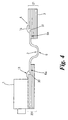
- the flexible circuit is deformed either during the transceiver assembly process or by pre-forming so that it bends 8 (like a caterpillar) to accommodate the differing optical-electrical subassembly separation 7
- the transmission lines on the flex are designed so that they support signal transmission over the full range of expected flex curvature. At the optical assembly end of the flex the transmission lines join the optical assembly with minimum electrical discontinuity. Careful selection of the dielectric constant of the flexible circuit minimizes electrical reflections across the interface.
- the mechanical attachment of the flexible circuit 2 to the optical subassembly 1 and electrical subassembly 3 is achieved using electrically conductive glue.
- Connection of the signal carrying traces 11, 12 on the top side of the flexible circuit 2 is then achieved using gold ribbon or gold wire bonds 13, 14.
- the uninterrupted groundplane connection is key to the performance of the electrical and optical subassembly interconnection.
- the use of multilayer construction 20, 21 of both the optical and electrical subassemblies respectively, enables the uninterrupted groundplane connection to be achieved.
- the multilayered subassemblies are preferable made of several layers of printed circuit boards. Alternatively, multiple layer of ceramic material can be used.
- step features 30, 31 are included in the multilayered subassemblies to facilitates connection of the flexible circuit to the subassemblies.
- the step features may be double step features.
- the present invention as described above and shown in figures 1-4 advantageously offers both electrical and mechanical benefits to fibre optic transceivers by ensuring good high frequency signal transmission and absorbing mechanical tolerances.
- the joining technique of the present invention provides for an uninterrupted low inductance groundplane.
Landscapes
- Physics & Mathematics (AREA)
- General Physics & Mathematics (AREA)
- Optics & Photonics (AREA)
- Engineering & Computer Science (AREA)
- Electromagnetism (AREA)
- Computer Networks & Wireless Communication (AREA)
- Signal Processing (AREA)
- Microelectronics & Electronic Packaging (AREA)
- Optical Couplings Of Light Guides (AREA)
- Semiconductor Lasers (AREA)
- Structure Of Printed Boards (AREA)
Abstract
Description
Claims (10)
- An optoelectronic module comprising an optical subassembly (1) and an electrical subassembly (3) each having a plurality of electrical connection points (4) and ground plane connection points (6a, 6b), characterized in that said optical and electrical subassemblies are connected by a flexible circuit (2), said flexible circuit comprising transmission lines (11,12) disposed on a substrate (15) having a groundplane (6), said connection being such that electrical connection of said groundplanes is established.
- A module as claimed in Claim 2, wherein said flexible circuit is connected to said optical and electrical subassemblies with electrically conductive glue.
- A module as claimed in Claim 3, wherein said transmission lines (11, 12) are electrically connected to said optical and electrical subassemblies with wire bonds (13, 14).
- A module as claimed in any preceding Claim, wherein said optical and/or electrical subassemblies are multi-layered structures (20, 21).
- A module as claimed in Claim 4, wherein said multilayer optical and/or electrical subassemblies (20, 21) include a step (30, 31) proximate said ground plane connection points (6a, 6b).
- A module as claimed in Claim 5, wherein said step (30, 31) is a double step.
- A module as claimed in any preceding Claims, wherein said module is a transmitter.
- A module as claimed in Claims 1-5, wherein said module is a receiver.
- A module as claimed in Claims 1-5, wherein said module is a transceiver.
- A module as claimed in any preceding Claim, wherein said transmission lines are capable of transmitting signals of at least 10 Giga Hertz.
Applications Claiming Priority (2)
| Application Number | Priority Date | Filing Date | Title |
|---|---|---|---|
| GBGB0123475.6A GB0123475D0 (en) | 2001-09-28 | 2001-09-28 | Flexible electrical interconnector for optical fibre transceivers |
| GB0123475 | 2001-09-29 |
Publications (2)
| Publication Number | Publication Date |
|---|---|
| EP1301061A2 true EP1301061A2 (en) | 2003-04-09 |
| EP1301061A3 EP1301061A3 (en) | 2003-11-12 |
Family
ID=9922975
Family Applications (1)
| Application Number | Title | Priority Date | Filing Date |
|---|---|---|---|
| EP02253646A Withdrawn EP1301061A3 (en) | 2001-09-28 | 2002-05-23 | Flexible electrical interconnect for optical fibre transceivers |
Country Status (3)
| Country | Link |
|---|---|
| US (1) | US20030063872A1 (en) |
| EP (1) | EP1301061A3 (en) |
| GB (1) | GB0123475D0 (en) |
Cited By (6)
| Publication number | Priority date | Publication date | Assignee | Title |
|---|---|---|---|---|
| WO2005025015A1 (en) * | 2003-09-01 | 2005-03-17 | Endress+Hauser Gmbh+Co. Kg | Field device for determining and/or monitoring a process variable |
| FR2867315A1 (en) * | 2004-03-02 | 2005-09-09 | Mitsubishi Electric Corp | OPTICAL SEMICONDUCTOR DEVICE |
| WO2007002628A3 (en) * | 2005-06-27 | 2007-03-29 | Intel Corp | Optical transponder module with dual board flexible circuit |
| DE102007062047A1 (en) * | 2007-12-21 | 2009-07-16 | Osram Opto Semiconductors Gmbh | compact housing |
| CN103178406A (en) * | 2011-12-22 | 2013-06-26 | 三菱电机株式会社 | Connection unit |
| EP2747528A1 (en) * | 2012-12-21 | 2014-06-25 | Thales | Interconnection device for electronic circuits, in particular hyperfrequency electronic circuits |
Families Citing this family (7)
| Publication number | Priority date | Publication date | Assignee | Title |
|---|---|---|---|---|
| US20040091268A1 (en) * | 2002-11-01 | 2004-05-13 | Jds Uniphase Corporation | Transmitter optical sub-assembly |
| US7717627B2 (en) * | 2003-12-29 | 2010-05-18 | Finisar Corporation | Electrical component connector with misalignment compensation |
| TWI244278B (en) | 2004-06-04 | 2005-11-21 | Ind Tech Res Inst | Optical transceiver module |
| CN101971414B (en) * | 2008-03-11 | 2013-09-25 | 富士通光器件株式会社 | Connection device and optical device |
| JP6272131B2 (en) * | 2014-05-02 | 2018-01-31 | 日本電信電話株式会社 | Optical module |
| CN207910042U (en) * | 2014-10-10 | 2018-09-25 | 株式会社村田制作所 | Transmission line and flat cable |
| JP7224921B2 (en) * | 2019-01-09 | 2023-02-20 | 日本ルメンタム株式会社 | Optical module and method for manufacturing optical module |
Family Cites Families (8)
| Publication number | Priority date | Publication date | Assignee | Title |
|---|---|---|---|---|
| GB9100815D0 (en) * | 1991-01-15 | 1991-02-27 | British Telecomm | Coplanar waveguide ribbon |
| JPH04349686A (en) * | 1991-05-28 | 1992-12-04 | Toshiba Corp | Chip carrier |
| JPH07162186A (en) * | 1993-12-08 | 1995-06-23 | Fujitsu Ltd | Optical transceiver unit |
| US5535043A (en) * | 1994-08-22 | 1996-07-09 | Hughes Aircraft Company | Replaceable actuator assembly for optical mirror with kinematic mount |
| JPH09148731A (en) * | 1995-11-17 | 1997-06-06 | Fujitsu Ltd | Method for manufacturing connection structure between wiring boards |
| JPH09148675A (en) * | 1995-11-21 | 1997-06-06 | Oki Electric Ind Co Ltd | Optical module mounting structure |
| JPH09172221A (en) * | 1995-12-18 | 1997-06-30 | Oki Electric Ind Co Ltd | Optical semiconductor element mounting structure |
| US6318902B1 (en) * | 1996-03-12 | 2001-11-20 | 3M Innovative Properties Company | Optical connector assembly using partial large diameter alignment features |
-
2001
- 2001-09-28 GB GBGB0123475.6A patent/GB0123475D0/en not_active Ceased
-
2002
- 2002-05-23 EP EP02253646A patent/EP1301061A3/en not_active Withdrawn
- 2002-09-27 US US10/256,780 patent/US20030063872A1/en not_active Abandoned
Cited By (11)
| Publication number | Priority date | Publication date | Assignee | Title |
|---|---|---|---|---|
| WO2005025015A1 (en) * | 2003-09-01 | 2005-03-17 | Endress+Hauser Gmbh+Co. Kg | Field device for determining and/or monitoring a process variable |
| FR2867315A1 (en) * | 2004-03-02 | 2005-09-09 | Mitsubishi Electric Corp | OPTICAL SEMICONDUCTOR DEVICE |
| WO2007002628A3 (en) * | 2005-06-27 | 2007-03-29 | Intel Corp | Optical transponder module with dual board flexible circuit |
| US7309173B2 (en) | 2005-06-27 | 2007-12-18 | Intel Corporation | Optical transponder module with dual board flexible circuit |
| DE102007062047A1 (en) * | 2007-12-21 | 2009-07-16 | Osram Opto Semiconductors Gmbh | compact housing |
| US8585257B2 (en) | 2007-12-21 | 2013-11-19 | Osram Opto Semiconductors Gmbh | Compact housing |
| CN103178406A (en) * | 2011-12-22 | 2013-06-26 | 三菱电机株式会社 | Connection unit |
| CN103178406B (en) * | 2011-12-22 | 2015-12-02 | 三菱电机株式会社 | connecting device |
| EP2747528A1 (en) * | 2012-12-21 | 2014-06-25 | Thales | Interconnection device for electronic circuits, in particular hyperfrequency electronic circuits |
| FR3000325A1 (en) * | 2012-12-21 | 2014-06-27 | Thales Sa | INTERCONNECTION DEVICE FOR ELECTRONIC CIRCUITS, ESPECIALLY HYPERFREQUENCY ELECTRONIC CIRCUITS |
| US8987887B2 (en) | 2012-12-21 | 2015-03-24 | Thales | Interconnection device for electronic circuits, notably microwave electronic circuits |
Also Published As
| Publication number | Publication date |
|---|---|
| GB0123475D0 (en) | 2001-11-21 |
| US20030063872A1 (en) | 2003-04-03 |
| EP1301061A3 (en) | 2003-11-12 |
Similar Documents
| Publication | Publication Date | Title |
|---|---|---|
| KR101234987B1 (en) | Flexible printed circuit board | |
| US7446261B2 (en) | Flexible circuit boards with tooling cutouts for optoelectronic modules | |
| US8044746B2 (en) | Flexible interconnect cable with first and second signal traces disposed between first and second ground traces so as to provide different line width and line spacing configurations | |
| US8847696B2 (en) | Flexible interconnect cable having signal trace pairs and ground layer pairs disposed on opposite sides of a flexible dielectric | |
| US6867668B1 (en) | High frequency signal transmission from the surface of a circuit substrate to a flexible interconnect cable | |
| US6797891B1 (en) | Flexible interconnect cable with high frequency electrical transmission line | |
| CN114730054B (en) | Integrated electro-optical flexible circuit board | |
| US7145411B1 (en) | Flexible differential interconnect cable with isolated high frequency electrical transmission line | |
| US5144691A (en) | Computer signal interconnect apparatus | |
| US7306377B2 (en) | Integrated optical sub-assembly having epoxy chip package | |
| US7336864B2 (en) | Opto-electronic board | |
| CN101971414B (en) | Connection device and optical device | |
| US20030063872A1 (en) | Flexible electrical interconnect for optical fibre transceivers | |
| US20190164891A1 (en) | Tunable differential via circuit | |
| JP2003279771A (en) | Optical waveguide device, photoelectric fusion substrate, high-speed optical serial bus, and manufacturing method thereof | |
| JP4816007B2 (en) | Flexible board connector, board connection structure, optical transceiver module and optical transceiver | |
| JP2007123742A (en) | Board connection structure, flex-rigid board, optical transceiver module and optical transceiver | |
| US11057984B2 (en) | High-speed hybrid circuit | |
| US20130011094A1 (en) | Opto-electric circuit board including metal-slotted optical waveguide and opto-electric simultaneous communication system | |
| JP2007123743A (en) | Flex-rigid board, optical transceiver module and optical transceiver | |
| US20220295630A1 (en) | Printed board and printed board assembly | |
| JP2006501517A (en) | High density fiber optic module with multiple folded flexible circuits | |
| EP1455208A1 (en) | Electrical connection arrangement, component and method, for instance for high speed optical transceivers | |
| KR100494473B1 (en) | Interconnection unit comprising optical PCB structure and data transmission system employing said interconnection unit | |
| US20020142626A1 (en) | Electrical interconnect structure |
Legal Events
| Date | Code | Title | Description |
|---|---|---|---|
| PUAI | Public reference made under article 153(3) epc to a published international application that has entered the european phase |
Free format text: ORIGINAL CODE: 0009012 |
|
| AK | Designated contracting states |
Kind code of ref document: A2 Designated state(s): AT BE CH CY DE DK ES FI FR GB GR IE IT LI LU MC NL PT SE TR Designated state(s): AT BE CH CY DE DK ES FI FR GB GR IE IT LI LU MC NL PT SE TR |
|
| AX | Request for extension of the european patent |
Extension state: AL LT LV MK RO SI |
|
| PUAL | Search report despatched |
Free format text: ORIGINAL CODE: 0009013 |
|
| AK | Designated contracting states |
Kind code of ref document: A3 Designated state(s): AT BE CH CY DE DK ES FI FR GB GR IE IT LI LU MC NL PT SE TR |
|
| AX | Request for extension of the european patent |
Extension state: AL LT LV MK RO SI |
|
| AKX | Designation fees paid | ||
| REG | Reference to a national code |
Ref country code: DE Ref legal event code: 8566 |
|
| STAA | Information on the status of an ep patent application or granted ep patent |
Free format text: STATUS: THE APPLICATION IS DEEMED TO BE WITHDRAWN |
|
| 18D | Application deemed to be withdrawn |
Effective date: 20040513 |