EP1300945A2 - Diamond substrate for surface acoustic wave device, and surface acoustic wave device - Google Patents
Diamond substrate for surface acoustic wave device, and surface acoustic wave device Download PDFInfo
- Publication number
- EP1300945A2 EP1300945A2 EP02256916A EP02256916A EP1300945A2 EP 1300945 A2 EP1300945 A2 EP 1300945A2 EP 02256916 A EP02256916 A EP 02256916A EP 02256916 A EP02256916 A EP 02256916A EP 1300945 A2 EP1300945 A2 EP 1300945A2
- Authority
- EP
- European Patent Office
- Prior art keywords
- diamond
- film
- diamond film
- saw
- propagation loss
- Prior art date
- Legal status (The legal status is an assumption and is not a legal conclusion. Google has not performed a legal analysis and makes no representation as to the accuracy of the status listed.)
- Withdrawn
Links
Images


Classifications
-
- H—ELECTRICITY
- H03—ELECTRONIC CIRCUITRY
- H03H—IMPEDANCE NETWORKS, e.g. RESONANT CIRCUITS; RESONATORS
- H03H9/00—Networks comprising electromechanical or electro-acoustic elements; Electromechanical resonators
- H03H9/46—Filters
- H03H9/64—Filters using surface acoustic waves
-
- H—ELECTRICITY
- H03—ELECTRONIC CIRCUITRY
- H03H—IMPEDANCE NETWORKS, e.g. RESONANT CIRCUITS; RESONATORS
- H03H9/00—Networks comprising electromechanical or electro-acoustic elements; Electromechanical resonators
- H03H9/02—Details
- H03H9/02535—Details of surface acoustic wave devices
- H03H9/02543—Characteristics of substrate, e.g. cutting angles
- H03H9/02582—Characteristics of substrate, e.g. cutting angles of diamond substrates
Definitions
- the present invention relates to a diamond substrate used for a surface acoustic wave (SAW) device applied to high-frequency filters or the like, and to a SAW device.
- SAW surface acoustic wave
- SAW devices applicable in the high frequency (e.g., 2.5 GHz) region.
- a typical example of the SAW devices is a SAW device in which interdigital electrodes (IDT: Inter-Digital Transducers) are formed on a piezoelectric layer, a surface acoustic wave is oscillated in the piezoelectric or a medium except for the piezoelectric by action of the interdigital transducer and the piezoelectric, and the surface acoustic wave is detected by the interdigital transducer and the piezoelectric.
- IDT Inter-Digital Transducers
- the conventional SAW devices applicable in the high frequency region were thus those in which the piezoelectric layer was formed on a thin film or diamond as a medium of SAW and in which the interdigital transducers were further formed on the piezoelectric layer.
- the diamond substrate for SAW device is desired to have the high propagation speed of SAW (preferably, 9000 m/s or higher), in order to enable use in the high frequency region.
- the present invention has been accomplished in order to solve the above problem and an object of the invention is to provide a SAW device diamond substrate and a surface acoustic wave device with a diamond film realizing the high propagation speed and small propagation loss of SAW.
- a SAW device diamond substrate is a diamond substrate for surface acoustic wave device comprising a substrate, and a diamond film formed on the substrate, wherein a hydrogen content of the diamond film is in the range of not less than 1% nor more than 5% in atomic percent and an arithmetic mean roughness (Ra) of a surface of the diamond film is not more than 20 nm.
- the surface acoustic wave is scattered more at grain boundaries because of high crystallinity in the diamond film, so as to increase the propagation loss.
- Fig. 1 is a schematic, perspective view of the SAW device 100 of the present embodiment.
- Fig. 2 is a sectional view along a line II-II of the SAW device 100 shown in Fig. 1.
- the SAW device 100 is composed of a diamond substrate 200 of the present embodiment, a piezoelectric film 120 formed on the diamond substrate 200 (an intermediate layer may also be formed between the diamond substrate 200 and the piezoelectric film 120), and an interdigital transducer 140 and an interdigital transducer 160 formed on the piezoelectric film 120.
- the diamond substrate 200 is comprised of a silicon wafer 220 and a diamond film 240.
- the diamond film 240 is formed on the surface of the silicon wafer 220 by CVD (chemical vapor deposition), hot-filament CVD, microwave plasma CVD, high-frequency plasma CVD, the DC plasma jet method, or the like. During the deposition of the film, the hydrogen content of the diamond film 240 is adjusted so as to fall in the range of not less than 1% nor more than 5% in atomic percent.
- the surface of the diamond film 240 thus deposited is smoothed by polishing so that the arithmetic mean roughness (Ra) thereof becomes not more than 20 nm (more preferably, not more than 10 nm).
- the polishing can be mechanical polishing by means of a grinding wheel including abrasive grains of diamond.
- the smoothing by polishing may be replaced by a method of micronizing grain sizes of crystals into the nanometer order during the deposition of the diamond film 240 so that the arithmetic mean roughness (Ra) becomes not more than 20 nm (more preferably, not more than 10 nm).
- the grinding wheel is preferably one in which the distance is small between the surface of the bond and the tip of the diamond abrasives and in which the diamond abrasives have a large area of a flat region at the distal end.
- the diamond film 240 satisfies the following conditions (1) to (4).
- the piezoelectric film 120 is formed on the surface of the diamond substrate 200 formed as described above, by CVD, microwave plasma CVD, PVD (physical vapor deposition), sputtering, ion plating, laser ablation, or the like.
- the piezoelectric can be one selected from AlN, ZnO, LiNbO 3 , LiTaO 3 , KNbO 3 , PZT (PbZr x Ti (1-x) O 3 ), and so on.
- the interdigital transducers 140 and 160 are formed on the surface of the piezoelectric film 120.
- the interdigital transducer 140 has an input terminal 142 and an input terminal 144, while the interdigital transducer 160 has an output terminal 162 and an output terminal 164.
- the SAW device of the present embodiment realizes the high propagation speed of the second-order Sezawa wave of 9000 m/s.
- the propagation speeds of quartz and LN used heretofore as SAW media are approximately 3900 m/s and 4700 m/s, respectively, whereas the propagation speed of 9000 m/s or higher is only one achieved by diamond with high elastic modulus.
- the diamond substrate of the present embodiment has the propagation loss of not more than 0.02 dB/ ⁇ when applied to the 2.5GHz SAW device, and the propagation loss of not more than 0.05 dB/ ⁇ when applied to the 5GHz SAW device.
- the present invention first realized such high propagation speed and small propagation losses, and this diamond substrate allows actualization of high-frequency devices with low loss.
- the insertion loss of the SAW device includes the resistance loss at the electrodes, the loss due to bidirectional spread of SAW, the loss due to reflection at the electrodes, the propagation loss, etc., and the present invention decreases the insertion loss of the SAW device on the basis of the decrease of propagation loss of the diamond substrate.
- the SAW devices were fabricated with different distances between the input and output electrodes (the SAW devices with the respective distances between the input and output electrodes equivalent to 50 waves, 100 waves, and 150 waves), and were evaluated as to the relation between insertion loss and propagation distance (the distance between the input and output electrodes). A linear relation was obtained between them. A propagation loss per wave was obtained from the slope of the straight line.
- the material of the substrate on which the diamond film is formed is not limited to Si, but may be one selected from ceramics and metals such as GaAs, SiC, AlN, InP, Si 3 N 4 , Mo, and so on.
- the diamond film 240 was formed in the thickness of 20 ⁇ m on the silicon wafer 220 0.8 mm thick, by filament CVD. A W wire was used as a filament. The temperature of the filament was controlled around 2100°C, and the temperature of the silicon wafer 220 around 800°C.
- the diamond substrate 200 obtained as described above was fixed to a metal holder, and thereafter the diamond film 240 was smoothed by mechanical polishing with the grinding wheel including the diamond abrasives.
- the grinding wheel used herein was one in which the average diameter of abrasives was 20 ⁇ m, the distance was 2 ⁇ m between the surface of the bond and the tip of the diamond abrasives, and the maximum length of flat regions at the distal end of the abrasives was 6 ⁇ m.
- the polishing conditions were that the number of rotation of the grinding wheel was 200 rpm, the number of rotation of the holder was 200 rpm, and the load was 4 kg. Table 1 presents the deposition conditions of the diamond film 240.
- a ZnO film (piezoelectric film 120) was then deposited in the thickness of 500 nm on the diamond film 240 after polished, by RF sputtering.
- Table 1 provides the results of the hydrogen content of the diamond film 240, the arithmetic mean roughness (Ra) of the surface thereof, and the propagation loss and propagation speed of SAW for each of examples and comparative examples.
- the hydrogen contents were determined by the method reported in JAPANESE JOURNAL OF APPLIED PHYSICS, VOL 23, No. 7, PP810-814, from absorption peaks of CH n near 3000 cm -1 in infrared absorption analysis..
- the arithmetic mean roughness (Ra) of the surface was determined by means of an atomic force microscope (AFM).
- the hydrogen content of the diamond film 240 was adjusted in the range of not less than 1% nor more than 5% in atomic percent and the surface was polished so that the arithmetic mean roughness (Ra) of the surface became not more than 20 nm, whereby the preferred propagation loss and propagation speed (the propagation loss of not more than 0.02 dB/ ⁇ and the propagation speed of not less than 9000 m/s for the 2.5GHz SAW) were successfully achieved.
- the preferred propagation loss and propagation speed the propagation loss of not more than 0.02 dB/ ⁇ and the propagation speed of not less than 9000 m/s for the 2.5GHz SAW
- Comparative Example 1-1 the hydrogen content was as small as 0.3%, and the surface acoustic wave was heavily scattered at grain boundaries, which posed the problem of increase of the propagation loss.
- Comparative Example 1-2 the arithmetic mean roughness (Ra) of the surface was as large as 25 nm, and the surface acoustic wave was heavily scattered, which posed the problem of increase of the propagation loss.
- Comparative Example 1-3 the hydrogen content was as large as 7%, and the decrease of hardness (decrease of elastic modulus) of the diamond film 240 posed the problem of decrease of the propagation speed.
- the diamond film 240 was deposited in the thickness of 20 ⁇ m on the silicon wafer 220 1.0 mm thick, by microwave CVD at the frequency of 2.45 GHz.
- the temperature of the silicon wafer 220 was controlled around 800°C.
- the surface of the diamond film 240 was smoothed by polishing in much the same manner as in Example 1.
- Table 2 presents the deposition conditions of the diamond film 240.
- the SAW device 100 was fabricated by applying the diamond substrate 200 in much the same manner as in Example 1.
- Table 2 provides the results of the hydrogen content of the diamond film 240, the arithmetic mean roughness (Ra) of the surface thereof, the half width of a peak in Raman spectroscopy, and the propagation loss and propagation speed of SAW for each of examples and comparative examples.
- Fig. 3 shows an example of a spectrum in the Raman spectroscopy of the diamond film. The peak near the wave number of 1333 cm -1 shown in Fig. 3 is a peak of diamond. The peak has some width because of the Raman effect.
- the crystallinity of the diamond film 240 was adjusted so that the half width of the peak became not less than 10 cm -1 , whereby the preferred propagation loss and propagation speed (the propagation loss of not more than 0.02 dB/ ⁇ and the propagation speed of not less than 9000 m/s for the 2.5GHz SAW) were successfully achieved.
- the preferred propagation loss and propagation speed the propagation loss of not more than 0.02 dB/ ⁇ and the propagation speed of not less than 9000 m/s for the 2.5GHz SAW
- the half width of the peak in Raman spectroscopy decreases.
- the surface acoustic wave is scattered more at grain boundaries, so as to increase the propagation loss.
- the diamond film 240 was formed in the thickness of 20 ⁇ m on the silicon wafer 220 0.8 mm thick, by filament CVD. A W wire was used as a filament. The temperature of the filament was controlled around 2100°C, and the temperature of the silicon wafer 220 around 800°C.
- the surface of the diamond film 240 was smoothed by polishing in much the same manner as in Example 1.
- Table 3 presents the deposition conditions of the diamond film 240.
- the SAW device 100 was fabricated by applying the diamond substrate 200 in much the same manner as in Example 1.
- Table 3 provides the results of the hydrogen content of the diamond film 240, the arithmetic mean roughness (Ra) of the surface thereof, the hardness thereof, and the propagation loss and propagation speed of SAW for each of examples and comparative examples.
- the hardness of the diamond film was adjusted so that the Knoop hardness of the diamond film 240 under the load of 500 g fell in the range of not less than 6000 kgf/mm 2 nor more than 8500 kgf/mm 2 , whereby the preferred propagation loss and propagation speed (the propagation loss of not more than 0.02 dB/ ⁇ and the propagation speed of not less than 9000 m/s for the 2.5GHz SAW) were successfully achieved.
- the preferred propagation loss and propagation speed the propagation loss of not more than 0.02 dB/ ⁇ and the propagation speed of not less than 9000 m/s for the 2.5GHz SAW
- the Knoop hardness under the load of 500 g was as small as 5200 kgf/mm 2 and the decrease of hardness (decrease of elastic modulus) of the diamond film 240 posed the problem of decrease of the propagation speed.
- the Knoop hardness under the load of 500 g was as large as 9600 kgf/mm 2 and the surface acoustic wave was heavily scattered at grain boundaries, which posed the problem of increase of the propagation loss.
- the propagation speed of SAW decreases.
- the hardness of the diamond film becomes higher on the other hand, i.e., as the crystallinity of the diamond film becomes better, the surface acoustic wave is scattered more at grain boundaries, so as to increase the propagation loss.
- the diamond film 240 was formed in the thickness of 20 ⁇ m on the silicon wafer 220 1.0 mm thick, by filament CVD. A W wire was used as a filament. The temperature of the filament was controlled around 2100°C, and the temperature of the silicon wafer 220 around 800°C.
- the surface of the diamond film 240 was smoothed by polishing in much the same manner as in Example 1.
- Table 4 presents the deposition conditions of the diamond film 240.
- the SAW device 100 was fabricated by applying the diamond substrate 200 in much the same manner as in Example 1.
- Table 4 provides the results of the hydrogen content of diamond crystals in the diamond film 240, the arithmetic mean roughness (Ra) of the surface, the mean particle size, and the propagation loss and propagation speed of SAW for each of examples and comparative examples.
- the grain sizes of crystals were determined with a scanning electron microscope (SEM).
- Fig. 4 shows an example of. observation of the diamond film with the scanning electron microscope (SEM).
- the average particle size of diamond crystals in the diamond film 240 was adjusted to be not more than 1 ⁇ m, whereby the preferred propagation loss and propagation speed (the propagation loss of not more than 0.02 dB/ ⁇ and the propagation speed of not less than 9000 m/s for the 2.50Hz SAW) were successfully achieved.
- the preferred propagation loss and propagation speed the propagation loss of not more than 0.02 dB/ ⁇ and the propagation speed of not less than 9000 m/s for the 2.50Hz SAW
- Comparative Example 4-1 and Comparative Example 4-2 the mean particle size of diamond crystals in the diamond film 240 was as large as 2.0 ⁇ m or 3.0 ⁇ m, respectively, and the surface acoustic wave became likely to be scattered, which posed the problem of increase of the propagation loss.
- the surface acoustic wave becomes more likely to be scattered, so as to increase the propagation loss.
- the diamond film 240 was formed in the thickness of 30 ⁇ m on the silicon wafer 220 1.2 mm thick, by filament CVD.
- a W wire was used as a filament.
- the temperature of the filament was controlled around 2100°C, and the temperature of the silicon wafer 220 around 800°C.
- the flow rate of hydrogen was 1500 sccm, that of methane 60 sccm, and the pressure 40 Torr.
- the diamond substrate 200 obtained as described above was fixed to the metal holder, and thereafter the diamond film 240 was smoothed by mechanical polishing with the grinding wheel including diamond abrasives.
- the grinding wheel used herein was one in which the mean diameter of abrasives was 20 ⁇ m.
- Table 5 presents the distance from the surface of the bond of the grinding wheel to the tip of the diamond abrasives, the maximum length of the flat regions at the distal ends of the abrasives, and the load during polishing.
- the polishing conditions were that the number of rotation of the grinding wheel was 200 rpm and the number of rotation of the holder 200 rpm.
- the SAW device 400 was fabricated by applying the diamond substrate 200, as in Example 1.
- Table 5 provides the results of the arithmetic mean roughness (Ra) of the surface of the diamond film 240 after smoothed by polishing, and the propagation loss and propagation speed of SAW for each of examples and a comparative example.
- the hydrogen content of the diamond film 240 was 2.5 atomic%.
- the arithmetic mean roughness (Ra) of the surface of the diamond film 240 was adjusted to be not more than 10 nm, whereby the extremely preferred propagation loss (the propagation loss of about 0.018 dB/ ⁇ for the 2.5 GHz SAW) was successfully achieved based on decrease in scattering of SAW.
- the extremely preferred propagation loss the propagation loss of about 0.018 dB/ ⁇ for the 2.5 GHz SAW
- the arithmetic mean roughness (Ra) of the surface of the diamond film 240 was as large as 26 nm and the surface acoustic wave was scattered more, so as to increase the propagation loss.
- the arithmetic mean roughness (Ra) of the surface of the diamond film 240 was as large as 14 nm and thus the effect of decreasing the propagation loss was relatively smaller.
- the diamond film 240 was formed in the thickness of 20 ⁇ m on the silicon wafer 220 0.8 mm thick, by filament CVD. A W wire was used as a filament. The temperature of the filament was controlled around 2100°C, and the temperature of the silicon wafer 220 around 800°C.
- the diamond substrate 200 obtained as described above was fixed to the metal holder, and thereafter the diamond film 240 was smoothed by mechanical polishing with the grinding wheel including the diamond abrasives.
- the grinding wheel used herein was one in which the average diameter of abrasives was 20 ⁇ m, the distance was 2 ⁇ m between the surface of the bond and the tip of the diamond abrasives, and the maximum length of flat regions at the distal end of the abrasives was 6 ⁇ m.
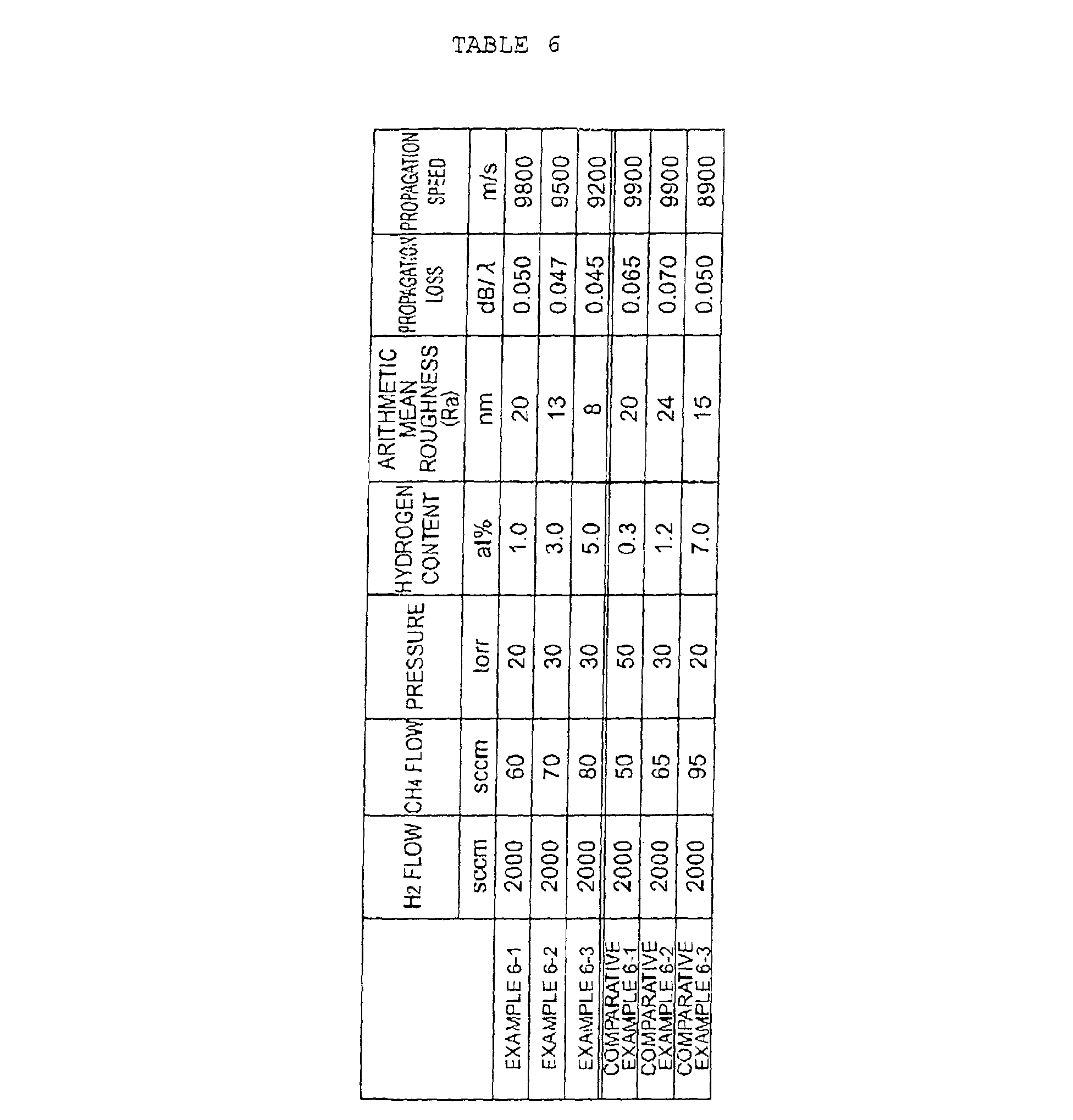
- the polishing conditions were that the number of rotation of the grinding wheel was 200 rpm, the number of rotation of the holder was 200 rpm, and the load was 3 kg. Table 6 presents the deposition conditions of the diamond film 240.
- a ZnO film (piezoelectric film 120) was then deposited in the thickness of 500 nm on the diamond film 240 after polished, by RF sputtering.
- An Al film was then formed in the thickness of 80 nm on the ZnO film by DC sputtering. Unnecessary portions were removed from the Al film by photolithography to form the interdigital transducers 140 and 160.
- the electrode width of the interdigital transducers 140 and 160 was 0.5 ⁇ m, the electrode cross width 50 times the wavelength ⁇ , and the number of electrode digit pairs 40.
- the characteristics of the SAW device 100 were evaluated by a network analyzer.
- Table 6 provides the results of the hydrogen content of the diamond film 240, the arithmetic mean roughness (Ra) of the surface thereof, and the propagation loss arid propagation speed of SAW for each of examples and comparative examples.
- the hydrogen content of the diamond film 240 was adjusted in the range of not less than 1% nor more than 5% in atomic percent and the surface was polished so that the arithmetic mean roughness (Ra) of the surface became not more than 20 nm, whereby the preferred propagation loss and propagation speed (the propagation loss of not more than 0.05 dB/ ⁇ and the propagation speed of not less than 9000 m/s for the 5GHz SAW) were successfully achieved.
- the preferred propagation loss and propagation speed the propagation loss of not more than 0.05 dB/ ⁇ and the propagation speed of not less than 9000 m/s for the 5GHz SAW
- Comparative Example 6-1 the hydrogen content was as small as 0.3%, and the surface acoustic wave was heavily scattered at grain boundaries, which posed the problem of increase of the propagation loss.
- Comparative Example 6-2 the arithmetic mean roughness (Ra) of the surface was as large as 24 nm, and the surface acoustic wave was largely scattered, which posed the problem of increase of the propagation loss.
- Comparative Example 6-3 the hydrogen content was as large as 7%, and the decrease of hardness (decrease of elastic modulus) of the diamond film 240 posed the problem of decrease of the propagation speed.
- the SAW device 100 is composed of a diamond substrate 200 of the present embodiment, a piezoelectric film 120 formed on the diamond substrate 200 (an intermediate layer may also be formed between the diamond substrate 200 and the piezoelectric film 120), and an interdigital transducer 140 and an interdigital transducer 160 formed on the piezoelectric film 120.
- the diamond substrate 200 is comprised of a silicon wafer 220 and a diamond film 240.
- the SAW device of the present invention may also be fabricated in such a way that the interdigital transducers are first formed on the diamond substrate and then the piezoelectric film is further formed on the diamond substrate.
- the diamond film 240 is formed on the surface of the silicon wafer 220 by CVD (chemical vapor deposition), hot-filament CVD, microwave plasma CVD, high-frequency plasma CVD, the DC plasma jet method, or the like.
- CVD chemical vapor deposition
- the hydrogen content of the diamond film 240 is adjusted in the range of not less than 1% nor more than 5% in atomic percent, and the ratio I (220) /I T of the peak intensity I (220) of the diamond crystal plane (220) to the total I r of the peak intensities of the diamond crystal planes (111), (220), (311), (400), and (331) in X-ray diffraction analysis is also adjusted so as to be not less than 0.8.
- Fig. 5 shows an example of an X-ray diffraction chart of the diamond substrate. In this example, I (220) /I T is 0.66, which is outside the range of the present embodiment.
- the surface of the diamond film 240 thus deposited is smoothed by polishing so that the arithmetic mean roughness (Ra) thereof becomes not more than 20 nm (more preferably, not more than 10 nm).
- the polishing can be mechanical polishing with the grinding stone including abrasive grains of diamond.
- the smoothing by polishing may be replaced by the method of micronizing grain sizes of crystals into the nanometer order during the deposition of the diamond film 240 so that the arithmetic mean roughness (Ra) becomes not more than 20 nm (more preferably, not more than 10 nm).
- the grinding wheel is preferably one in which the distance is small between the surface of the bond and the flat surfaces at the tip of the diamond abrasives and in which the diamond abrasives have large areas of the flat surfaces at the tip of the diamond abrasives.
- the material of the substrate for the diamond film 240 to be formed thereon is not limited to silicon, but can be one of ceramics and metals such as Si 3 N 4 , Mo, etc., in addition to GaAs, SiC, AlN, InP, GaN, and so on.
- the material can also be cemented carbide or cermet, depending upon applications.
- the diamond film 240 satisfies the following conditions (1) to (3).
- the piezoelectric film 120 is formed on the surface of the diamond substrate 200 formed as described above, by CVD, microwave plasma CVD, PVD (physical vapor deposition), sputtering, ion plating, laser ablation, or the like.
- the piezoelectric can be one selected from AlN, ZnO, LiNbO 3 , LiTaO 3 , KNbO 3 , PZT (PbZr x Ti (1-x) O 3 ), and so on.
- the interdigital transducers 140 and 160 are formed on the surface of the piezoelectric film 120.
- the interdigital transducer 140 has an input terminal 142 and an input terminal 144, while the interdigital transducer 160 has an output terminal 162 and an output terminal 164.
- the diamond substrate 200 of the present embodiment achieves the high propagation speed of the second-order Sezawa wave of 9000 m/s, because the hydrogen content of the diamond film 240 is not more than 5% in atomic percent.
- the diamond substrate 200 demonstrates the propagation loss of not more than 0.022 dB/ ⁇ in application to the 2.5GHz SAW device, because the hydrogen content of the diamond film 240 is not less than 1% in atomic percent; and the diamond substrate 200 has the Q value of not less than 700, because the intensity ratio (I (220) /I T ) of the plane (220) is not less than 0.8.
- Such high propagation speed, small propagation loss, and large Q value were first substantiated simultaneously by the present invention, and this diamond substrate made it feasible to realize the SAW devices ready for high frequencies with low loss and with excellent frequency characteristics.
- the insertion loss of the SAW device includes the resistance loss at the electrodes, the loss due to bidirectional spread of SAW, the loss due to reflection at the electrodes, the propagation loss, etc., and the present invention decreases the insertion loss of SAW on the basis of the decrease of propagation loss of the diamond substrate.
- the SAW devices were fabricated with different distances between the input and output electrodes (the SAW devices with the respective distances between the input and output electrodes equivalent to 50 waves, 100 waves, and 150 waves), and were evaluated as to the relation between insertion loss and propagation distance (the distance between the input and output electrodes). A linear relation was obtained between them. A propagation loss per wave was obtained from the slope of the straight line. Also, Inventors calculated the analyzed propagation loss based on the actual insertion loss measured at frequency between 2.3 - 2.6 GHz. The analyzed propagation loss 0.022 dB/ ⁇ is equivalent to the actual propagation loss at frequency 2.5 GHz 0.02 dB/ ⁇ .
- the "propagation loss” is represented by the analyzed propagation loss.
- the diamond film 240 was formed in the thickness of 20 ⁇ m on the silicon wafer 220 0.8 mm thick, by filament CVD.
- a W wire was used as a filament.
- the temperature of the filament was controlled approximately in the range of 2100 to 2200°C, and the temperature of the silicon wafer 220 approximately in the range of 700 to 800°C.
- Source gases were hydrogen and methane.
- the flow rate of hydrogen gas was determined in the range of 500 to 5000 sccm, and the percent of the flow rate of methane gas to the flow rate of hydrogen gas in the range of 0.5 to 5.0%.
- the pressure of gas was determined in the range of 5 to 120 Torr.
- the diamond substrate 200 obtained as described above was fixed to the metal holder, and thereafter the diamond film 240 was smoothed by mechanical polishing with the grinding wheel including the diamond abrasives.
- the grinding wheel used herein was one in which the average diameter of diamond abrasives was 20 ⁇ m, the distance was 2 ⁇ m between the surface of the bond and the flat surfaces at the Lip of the diamond abrasives, and the maximum length of the flat surfaces at the tip of the diamond abrasives was 6 ⁇ m.
- the polishing conditions were that the number of rotation of the grinding wheel was 200 rpm, the number of rotation of the holder was 200 rpm, and the load was 4 kg.
- a ZnO film (piezoelectric film 120) was then deposited in the thickness of 500 nm on the diamond film 240 after polished, by RF sputtering.
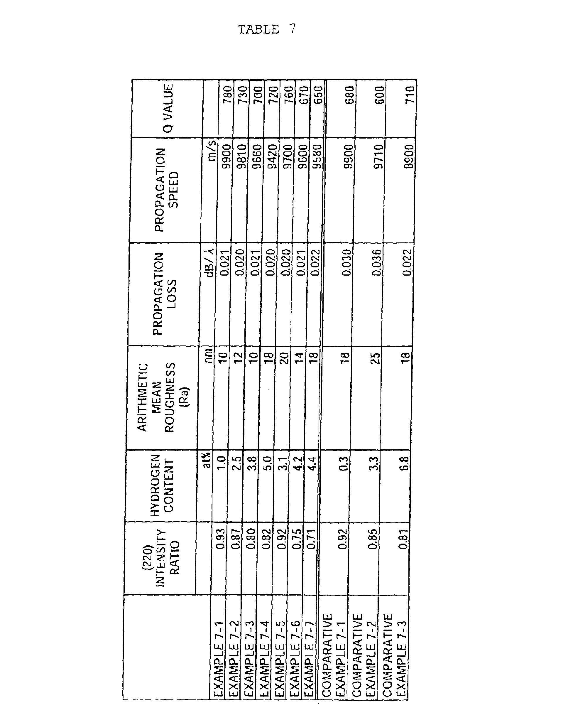
- Table 7 provides the results of the intensity ratio of the plane (220) of the diamond film 240, the hydrogen content (atomic percent), the arithmetic mean roughness (Ra) of the surface thereof, the propagation loss and propagation speed of SAW, and the Q value for each of examples and comparative examples.
- the hydrogen contents were determined by the method reported in JAPANESE JOURNAL OF APPLIED PHYSICS, VOL 23, No. 7, PP810-814, from absorption peaks of CH n near 3000 cm -1 in infrared absorption analysis.
- the arithmetic mean roughness (Ra) of the surface was determined by means of the atomic force microscope (AFM) .
- the intensity ratio of (220) of the diamond film 240 was adjusted in the range of not less than 0.80, the hydrogen content was adjusted in the range of not less than 1% nor more than 5% in atomic percent, and the surface was polished so as to have the arithmetic mean roughness (Ra) of not more than 20 nm, whereby the preferred propagation loss, propagation speed, and Q value (the propagation loss of not more than 0.022 dB/ ⁇ and the propagation speed of the second-order Sezawa wave of not less than 9000 m/s for the 2.5GHz SAW, and the Q value of not less than 700) were successfully achieved.
- Ra arithmetic mean roughness
- the (220) intensity ratio was as small as 0.75 or 0.71, respectively, so that the Q value was small, but the propagation loss and propagation speed were satisfactory.
- the hydrogen content was as low as 0.3%, and the surface acoustic wave was heavily scattered at grain boundaries, which posed the problem of increase of the propagation loss.
- the arithmetic mean roughness (Ra) of the surface was as large as 25 nm, so that the surface acoustic wave was heavily scattered, so as to pose the problem of increase of the propagation loss.
- the hydrogen content was as large as 6.8%, and the decrease of hardness (decrease of elastic modulus) of the diamond film 240 posed the problem of decrease of the propagation speed.
- the Q value was increased to the preferred level with the preferred propagation speed and propagation loss of SAW being maintaining, when the ratio I (220) /I T of the peak intensity I (220) of the diamond crystal plane (220) to the total I T of the peak intensities of the diamond crystal planes (111), (220), (311), (400), and (331) in X-ray diffraction analysis of the diamond film, was not less than 0.8.
- the diamond film 240 was formed in the thickness of 20 ⁇ m on the silicon wafer 220 1.0 mm thick, by microwave CVD at the frequency of 2.45 GHz.
- the temperature of the silicon wafer 220 was controlled approximately in the range of 700 to 800°C.
- Source gases were hydrogen and methane.
- the flow rate of hydrogen gas was determined in the range of 500 to 5000 sccm, and the percent of the flow rate of methane gas to the flow rate of hydrogen gas in the range of 0.5 to 5.0%.
- the pressure of gas was determined in the range of 5 to 120 Torr.
- the surface of the diamond film 240 was smoothed by polishing in much the same manner as in Example 7.
- the SAW device 100 was fabricated by applying the diamond substrate 200 in much the same manner as in Example 7.
- Table 8 provides the results of the (220) intensity ratio of the diamond film 240, the hydrogen content, the arithmetic mean roughness (Ra) of the surface, the half width of the peak in Raman spectroscopy, the propagation loss and propagation speed of SAW, and the Q value for each of examples and comparative examples.
- Fig. 3 shows an example of the spectrum in Raman spectroscopy of the diamond film. The peak near the wave number of 1333 cm -1 shown in Fig. 3 is a peak of diamond. The peak has some width because of the Raman effect.
- the crystallinity of the diamond film 240 was adjusted so that the half width of the peak became not less than 10 cm -1 , whereby the preferred propagation loss, propagation speed, and Q value (the propagation loss of not more than 0.022 dB/ ⁇ and the propagation speed of the second-order Sezawa wave of not less than 9000 m/s for the 2.5GHz SAW, and the Q value of not less than 700) were successfully achieved.
- the preferred propagation loss, propagation speed, and Q value the propagation loss of not more than 0.022 dB/ ⁇ and the propagation speed of the second-order Sezawa wave of not less than 9000 m/s for the 2.5GHz SAW, and the Q value of not less than 700
- Example 8-4 the substrate demonstrated the preferred values of the (220) intensity ratio, hydrogen content, and surface roughness (Ra) but had the small half width of 9 cm -1 , so that the effect of decreasing the propagation loss was relatively smaller.
- the diamond film 240 was formed in the thickness of 20 ⁇ m on the silicon wafer 220 0.8 mm thick, by filament CVD.
- a W wire was used as a filament.
- the temperature of the filament was controlled approximately in the range of 2100 to 2200°C, and the temperature of the silicon wafer 220 approximately in the range of 700 to 800°C.
- Source gases were hydrogen and methane.
- the flow rate of hydrogen gas was determined in the range of 500 to 5000 sccm, and the percent of the flow rate of methane gas to the flow rate of hydrogen gas in the range of 0.5 to 5.0%.
- the pressure of gas was determined in the range of 5 to 120 Torr.
- the surface of the diamond film 240 was smoothed by polishing in much the same manner as in Example 7.
- the SAW device 100 was fabricated by applying the diamond substrate 200 in much the same manner as in Example 7.
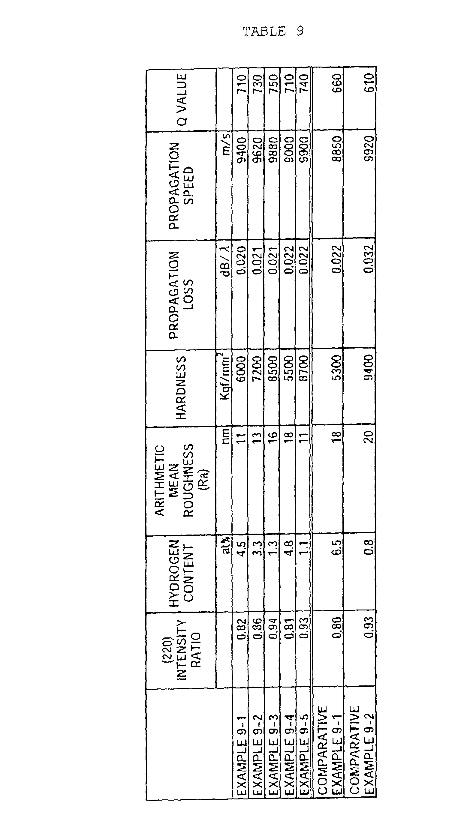
- Table 9 provides the results of the (220) intensity ratio of the diamond film 240, the hydrogen content, the arithmetic mean roughness (Ra) of the surface, the hardness (the Knoop hardness measured under the load of 500 g), the propagation loss and propagation speed of SAW, and the Q value for each of examples and comparative examples.
- the diamond film 240 was adjusted so that the Knoop hardness thereof measured under the load of 500 g fell in the range of not less than 6000 kgf/mm 2 nor more than 8500 kgf/mm 2 , whereby the preferred propagation loss, propagation speed, and Q value (the propagation loss of not more than 0.022 dB/ ⁇ and the propagation speed of the second-order Sezawa wave of not less than 9000 m/s for the 2.5GHz SAW, and the Q value of not less than 700) were successfully achieved.
- the preferred propagation loss, propagation speed, and Q value the propagation loss of not more than 0.022 dB/ ⁇ and the propagation speed of the second-order Sezawa wave of not less than 9000 m/s for the 2.5GHz SAW, and the Q value of not less than 700
- Example 9-1 the Knoop hardness under the load of 500 g was as small as 5300 kgf/mm 2 , and there arose the problem of decrease of the propagation speed.
- Comparative Example 9-2 the Knoop hardness under the load of 500 g was as large as 9400 kgf/mm 2 , and the surface acoustic wave was heavily scattered at grain boundaries, so as to pose the problem of increase of the propagation loss.
- Example 9-4 the substrate demonstrated the preferred values of the (220) intensity ratio, hydrogen content, and surface roughness (Ra) but had the small Knoop hardness of 5500 kgf/mm 2 under the load of 500 g, so that the effect of increasing the propagation speed was relatively smaller.
- Example 9-5 the substrate demonstrated the preferred values of the (220) intensity ratio, hydrogen content, and surface roughness (Ra) but had the large Knoop hardness of 8700 kgf/mm 2 under the load of 500 g, though the surface was flatly polished to the surface roughness (Ra) of 11. Therefore, the substrate of Example 9-5 exhibited the relatively smaller effect of decreasing the propagation loss.
- the diamond film 240 was formed in the thickness of 20 ⁇ m on the silicon wafer 220 1.0 mm thick, by filament CVD.
- a W wire was used as a filament.
- the temperature of the filament was controlled approximately in the range of 2100 to 2200°C, and the temperature of the silicon wafer 220 approximately in the range of 700 to 800°C.
- Source gases were hydrogen and methane.
- the flow rate of hydrogen gas was determined in the range of 500 to 5000 sccm, and the percent of the flow rate of methane gas to the flow rate of hydrogen gas in the range of 0.5 to 5.0%.
- the pressure of gas was determined in the range of 5 to 120 Torr.
- the surface of the diamond film 240 was smoothed by polishing in much the same manner as in Example 7.
- the SAW device 100 was fabricated by applying the diamond substrate 200 in much the same manner as in Example 7.
- Table 10 provides the results of the (220) intensity ratio of the diamond film 240, the hydrogen content, the arithmetic mean roughness (Ra) of the surface, the mean particle size of diamond crystals, the propagation loss and propagation speed of SAW, and the Q value for each of examples and comparative examples.
- the grain sizes of crystals were measured by means of the scanning electron microscope (SEM).
- Fig. 4 shows the example of observation of the diamond film with the scanning electron microscope (SEM).
- the diamond film 240 was adjusted so that the mean particle size of diamond crystals therein became not more than 1 ⁇ m, whereby the preferred propagation loss, propagation speed, and Q value (the propagation loss of not more than 0.022 dB/ ⁇ and the propagation speed of the second-order Sezawa wave of not less than 9000 m/s for the 2.5GHz SAW, and the Q value of not loss than 700) were successfully achieved.
- the preferred propagation loss, propagation speed, and Q value the propagation loss of not more than 0.022 dB/ ⁇ and the propagation speed of the second-order Sezawa wave of not less than 9000 m/s for the 2.5GHz SAW, and the Q value of not loss than 700
- Example 10-4 the substrate demonstrated the preferred values of the (220) intensity ratio, hydrogen content, and surface roughness (Ra), but had the large mean particle size of diamond crystals of 2.0 ⁇ m in the diamond film 240, so that the effect of decreasing the propagation loss was relatively smaller.
- the diamond film 240 was formed in the thickness of 30 ⁇ m on the silicon wafer 220 1.2 mm thick, by filament CVD.
- a W wire was used as a filament.
- the temperature of the filament was controlled approximately in the range of 2100 to 2200°C, and the temperature of the silicon wafer 220 approximately in the range of 700 to 800°C.
- Source gases were hydrogen and methane.
- the flow rate of hydrogen gas was 1500 sccm and the flow rate of methane gas 60 sccm.
- the pressure of gas was 20 Torr.
- the diamond substrate 200 was fixed to the metal holder and thereafter the diamond film 240 was smoothed by mechanical polishing with the grinding wheel including the diamond abrasives in the average diameter of 30 ⁇ m.
- Table 11 presents the distance between the surface of the bond and the flat surfaces at the tip of the diamond abrasives in the grinding wheel, the maximum length of the flat surfaces at the tip of the diamond abrasives, and the load during the polishing.
- the polishing conditions were that the number of rotation of the grinding wheel was 200 rpm and the number of rotation of the holder 200 rpm.
- the SAW device 100 was fabricated by applying the diamond substrate 200 in much the same manner as in Example 7.
- Table 11 provides the results of the arithmetic mean roughness (Ra) of the surface of the diamond film 240, the propagation loss and propagation speed of SAW, and the Q value for each of examples and a comparative example.
- the diamond film 240 was adjusted so that the arithmetic mean roughness (Ra) of the surface thereof became not more than 10 nm, whereby the extremely preferred propagation loss (the propagation loss of about 0.019 dB/ ⁇ for the 2.5 GHz SAW) was successfully achieved based on decrease in scattering of SAW.
- the extremely preferred propagation loss the propagation loss of about 0.019 dB/ ⁇ for the 2.5 GHz SAW
- Example 11-1 the arithmetic mean roughness (Ra) of the surface of the diamond film 240 was as large as 26 nm arid the surface acoustic wave was scattered more, so as to increase the propagation loss.
- Example 11-4 the arithmetic mean roughness (Ra) of the surface of the diamond film 240 was as large as 15 nm and thus the effect of decreasing the propagation loss was relatively smaller.
Landscapes
- Physics & Mathematics (AREA)
- Acoustics & Sound (AREA)
- Surface Acoustic Wave Elements And Circuit Networks Thereof (AREA)
- Crystals, And After-Treatments Of Crystals (AREA)
- Chemical Vapour Deposition (AREA)
Abstract
Description





Claims (8)
- A diamond substrate for surface acoustic wave device, comprising a substrate, and a diamond film formed on the substrate,
wherein a hydrogen content of said diamond film is in the range of not less than 1% nor more than 5% in atomic percent, and
wherein an arithmetic mean roughness (Ra) of a surface of said diamond film is not more than 20 nm. - The diamond substrate according to Claim 1, wherein a ratio I(220)/IT, which is a ratio of a peak intensity I(220) of the diamond crystal plane (220) to the total IT of peak intensities of the diamond crystal planes (111), (220), (311), (400), and (331) in X-ray diffraction analysis of said diamond film, is not less than 0.8.
- The diamond substrate according to Claim 1 or 2, wherein said diamond film has a peak near the wave number of 1333 cm-1 in Raman spectroscopy and a half width of said peak is not less than 10 cm-1.
- The diamond substrate according to Claim 1 or 2, wherein a Knoop hardness of said diamond film measured under a load of 500 g is in the range of not less than 6000 kgf/mm2 nor more than 8500 kgf/mm2.
- The diamond substrate according to Claim 1 or 2, wherein a mean particle size of diamond crystals in said diamond film is not more than 1 µm.
- The diamond substrate according to Claim 1 or 2, wherein the arithmetic mean roughness (Ra) of the surface of said diamond film is not more than 10 nm.
- A surface acoustic wave device in which a piezoelectric film is formed on the diamond substrate as set forth in one of Claims 1 to 6 and in which interdigital transducers are formed on said piezoelectric film.
- The surface acoustic wave device according to Claim 7, wherein a propagation loss of the second-order Sezawa wave of 2.5 GHz propagating in said diamond film is not more than 0.02 dB/λ and a propagation speed thereof is not less than 9000 m/s.
Applications Claiming Priority (4)
| Application Number | Priority Date | Filing Date | Title |
|---|---|---|---|
| JP2001310370 | 2001-10-05 | ||
| JP2001310370A JP2003112995A (en) | 2001-10-05 | 2001-10-05 | Diamond substrate for surface acoustic wave device and surface acoustic wave device |
| JP2002022249 | 2002-01-30 | ||
| JP2002022249A JP2003221294A (en) | 2002-01-30 | 2002-01-30 | Diamond substrate for surface acoustic wave device and surface acoustic wave device |
Publications (2)
| Publication Number | Publication Date |
|---|---|
| EP1300945A2 true EP1300945A2 (en) | 2003-04-09 |
| EP1300945A3 EP1300945A3 (en) | 2004-05-06 |
Family
ID=26623779
Family Applications (1)
| Application Number | Title | Priority Date | Filing Date |
|---|---|---|---|
| EP02256916A Withdrawn EP1300945A3 (en) | 2001-10-05 | 2002-10-04 | Diamond substrate for surface acoustic wave device, and surface acoustic wave device |
Country Status (4)
| Country | Link |
|---|---|
| US (1) | US6661152B2 (en) |
| EP (1) | EP1300945A3 (en) |
| KR (1) | KR100858600B1 (en) |
| TW (1) | TWI264869B (en) |
Cited By (1)
| Publication number | Priority date | Publication date | Assignee | Title |
|---|---|---|---|---|
| CN103918096A (en) * | 2011-10-28 | 2014-07-09 | 印度马德拉斯理工学院 | Piezoelectric devices and methods of making and using same |
Families Citing this family (7)
| Publication number | Priority date | Publication date | Assignee | Title |
|---|---|---|---|---|
| DE102005001097A1 (en) * | 2005-01-08 | 2006-07-27 | Abb Patent Gmbh | Pressure sensor (I) |
| CN100530956C (en) * | 2005-10-19 | 2009-08-19 | 鸿富锦精密工业(深圳)有限公司 | Surface acoustic wave part |
| CN102286722B (en) * | 2011-06-15 | 2014-04-16 | 南京理工大学 | Preparation method of zinc oxide/diamond-like carbon surface acoustic wave device composite film |
| WO2014027538A1 (en) * | 2012-08-17 | 2014-02-20 | 日本碍子株式会社 | Composite substrate, elastic surface wave device, and method for producing composite substrate |
| WO2014188842A1 (en) * | 2013-05-21 | 2014-11-27 | 日本碍子株式会社 | Method for manufacturing piezoelectric device, piezoelectric device, and piezoelectric free-standing substrate |
| US10494713B2 (en) | 2015-04-16 | 2019-12-03 | Ii-Vi Incorporated | Method of forming an optically-finished thin diamond film, diamond substrate, or diamond window of high aspect ratio |
| US11588463B2 (en) * | 2020-09-24 | 2023-02-21 | Huawei Technologies Co., Ltd. | Surface acoustic wave devices with ultra-thin transducers |
Family Cites Families (14)
| Publication number | Priority date | Publication date | Assignee | Title |
|---|---|---|---|---|
| US5284525A (en) * | 1990-12-13 | 1994-02-08 | Canon Kabushiki Kaisha | Solar cell |
| JP3110491B2 (en) * | 1991-05-17 | 2000-11-20 | ティーディーケイ株式会社 | Surface acoustic wave device using diamond-like film |
| JPH04358410A (en) * | 1991-06-05 | 1992-12-11 | Sumitomo Electric Ind Ltd | Surface acoustic wave element and production thereof |
| US5225926A (en) * | 1991-09-04 | 1993-07-06 | International Business Machines Corporation | Durable optical elements fabricated from free standing polycrystalline diamond and non-hydrogenated amorphous diamond like carbon (dlc) thin films |
| JP3295921B2 (en) * | 1994-06-20 | 2002-06-24 | 住友電気工業株式会社 | Diamond substrate for surface acoustic wave device and device |
| JP3416470B2 (en) * | 1996-07-18 | 2003-06-16 | 三洋電機株式会社 | Surface acoustic wave device |
| JPH1082390A (en) * | 1996-07-18 | 1998-03-31 | Sanyo Electric Co Ltd | Sliding member, compressor and rotary compressor |
| JP3609591B2 (en) * | 1997-09-25 | 2005-01-12 | 三洋電機株式会社 | Hard carbon thin film and manufacturing method thereof |
| JP3755559B2 (en) * | 1997-04-15 | 2006-03-15 | 株式会社日鉱マテリアルズ | Sputtering target |
| JP3168961B2 (en) * | 1997-10-06 | 2001-05-21 | 住友電気工業株式会社 | Diamond substrate, method for evaluating diamond substrate, and diamond surface acoustic wave filter |
| JPH11292692A (en) * | 1998-04-07 | 1999-10-26 | Sumitomo Electric Ind Ltd | Hard carbon film and hard carbon substrate |
| JP3189833B2 (en) * | 1998-10-30 | 2001-07-16 | 住友電気工業株式会社 | Hard carbon film and substrate for surface acoustic wave device |
| US6416865B1 (en) * | 1998-10-30 | 2002-07-09 | Sumitomo Electric Industries, Ltd. | Hard carbon film and surface acoustic-wave substrate |
| JP3341759B2 (en) * | 1999-10-15 | 2002-11-05 | 住友電気工業株式会社 | Surface acoustic wave device |
-
2002
- 2002-10-04 KR KR1020020060541A patent/KR100858600B1/en not_active Expired - Fee Related
- 2002-10-04 US US10/264,264 patent/US6661152B2/en not_active Expired - Fee Related
- 2002-10-04 EP EP02256916A patent/EP1300945A3/en not_active Withdrawn
- 2002-10-04 TW TW091122997A patent/TWI264869B/en active
Cited By (4)
| Publication number | Priority date | Publication date | Assignee | Title |
|---|---|---|---|---|
| CN103918096A (en) * | 2011-10-28 | 2014-07-09 | 印度马德拉斯理工学院 | Piezoelectric devices and methods of making and using same |
| US9362378B2 (en) | 2011-10-28 | 2016-06-07 | Indian Institute Of Technology Madras | Piezoelectric devices and methods for their preparation and use |
| US9882116B2 (en) | 2011-10-28 | 2018-01-30 | Indian Institute Of Technology Madras | Piezoelectric devices and methods for their preparation and use |
| CN103918096B (en) * | 2011-10-28 | 2018-09-28 | 印度马德拉斯理工学院 | Piezoelectric device and its preparation and application |
Also Published As
| Publication number | Publication date |
|---|---|
| US20030137217A1 (en) | 2003-07-24 |
| TWI264869B (en) | 2006-10-21 |
| KR20030029505A (en) | 2003-04-14 |
| EP1300945A3 (en) | 2004-05-06 |
| US6661152B2 (en) | 2003-12-09 |
| KR100858600B1 (en) | 2008-09-17 |
Similar Documents
| Publication | Publication Date | Title |
|---|---|---|
| US7579759B2 (en) | Surface acoustic wave (SAW) devices based on cubic boron nitride/diamond composite structures | |
| US7011134B2 (en) | Casting method for producing surface acoustic wave devices | |
| US5355568A (en) | Method of making a surface acoustic wave device | |
| Nakahata et al. | High frequency surface acoustic wave filter using ZnO/diamond/Si structure | |
| EP0674385B1 (en) | Orientational material, orientational substrate and surface acoustic wave device | |
| Okano et al. | Preparation of aluminum nitride thin films by reactive sputtering and their applications to GHz‐band surface acoustic wave devices | |
| EP1001048B1 (en) | Surface-acoustic-wave substrate having hard carbon film | |
| US6661152B2 (en) | Diamond substrate for surface acoustic wave device, and surface acoustic wave device | |
| US6858969B2 (en) | Surface acoustic wave devices based on unpolished nanocrystalline diamond | |
| JP2020061684A (en) | Composite substrate for surface acoustic wave element and production method thereof | |
| JPH10270978A (en) | Surface acoustic wave device and method of manufacturing the same | |
| Shikata et al. | 1.5 GHz SAW bandpass filter using poly-crystalline diamond | |
| JP2003221294A (en) | Diamond substrate for surface acoustic wave device and surface acoustic wave device | |
| US20250023551A1 (en) | Joint body and elastic wave element | |
| JP2003112995A (en) | Diamond substrate for surface acoustic wave device and surface acoustic wave device | |
| Nakahata et al. | Fabrication of 2.5 GHz SAW retiming filter with SiO/sub 2//ZnO/diamond structure | |
| JPH08148957A (en) | Piezoelectric thin film wafer and manufacturing method thereof | |
| Liaw et al. | The SAW characteristics of sputtered aluminum nitride on silicon | |
| Uemura et al. | Low loss diamond SAW devices by small grain size poly-crystalline diamond | |
| Fujii et al. | Diamond wafer for SAW application | |
| EP0644651B1 (en) | Surface wave filter element and method for manufacturing it | |
| JP2003234631A (en) | Diamond composite, surface acoustic wave device, and method for producing diamond composite | |
| JP3132065B2 (en) | Surface acoustic wave device and method of manufacturing the same | |
| JPH11292692A (en) | Hard carbon film and hard carbon substrate | |
| JP3189833B2 (en) | Hard carbon film and substrate for surface acoustic wave device |
Legal Events
| Date | Code | Title | Description |
|---|---|---|---|
| PUAI | Public reference made under article 153(3) epc to a published international application that has entered the european phase |
Free format text: ORIGINAL CODE: 0009012 |
|
| AK | Designated contracting states |
Kind code of ref document: A2 Designated state(s): AT BE BG CH CY CZ DE DK EE ES FI FR GB GR IE IT LI LU MC NL PT SE SK TR Designated state(s): AT BE BG CH CY CZ DE DK EE ES FI FR GB GR IE IT LI LU MC NL PT SE SK TR |
|
| AX | Request for extension of the european patent |
Extension state: AL LT LV MK RO SI |
|
| PUAL | Search report despatched |
Free format text: ORIGINAL CODE: 0009013 |
|
| AK | Designated contracting states |
Kind code of ref document: A3 Designated state(s): AT BE BG CH CY CZ DE DK EE ES FI FR GB GR IE IT LI LU MC NL PT SE SK TR |
|
| AX | Request for extension of the european patent |
Extension state: AL LT LV MK RO SI |
|
| 17P | Request for examination filed |
Effective date: 20040929 |
|
| AKX | Designation fees paid |
Designated state(s): DE FR GB |
|
| 17Q | First examination report despatched |
Effective date: 20080415 |
|
| STAA | Information on the status of an ep patent application or granted ep patent |
Free format text: STATUS: THE APPLICATION IS DEEMED TO BE WITHDRAWN |
|
| 18D | Application deemed to be withdrawn |
Effective date: 20080826 |