EP1298634A2 - Active matrix type display device - Google Patents
Active matrix type display device Download PDFInfo
- Publication number
- EP1298634A2 EP1298634A2 EP02256758A EP02256758A EP1298634A2 EP 1298634 A2 EP1298634 A2 EP 1298634A2 EP 02256758 A EP02256758 A EP 02256758A EP 02256758 A EP02256758 A EP 02256758A EP 1298634 A2 EP1298634 A2 EP 1298634A2
- Authority
- EP
- European Patent Office
- Prior art keywords
- pixel
- power supply
- thin film
- film transistor
- supply line
- Prior art date
- Legal status (The legal status is an assumption and is not a legal conclusion. Google has not performed a legal analysis and makes no representation as to the accuracy of the status listed.)
- Withdrawn
Links
- 239000011159 matrix material Substances 0.000 title claims abstract description 46
- 239000010409 thin film Substances 0.000 claims description 50
- 239000010410 layer Substances 0.000 description 60
- 239000000463 material Substances 0.000 description 19
- 230000015572 biosynthetic process Effects 0.000 description 16
- 239000003990 capacitor Substances 0.000 description 15
- 239000010408 film Substances 0.000 description 13
- 239000000758 substrate Substances 0.000 description 10
- 230000005525 hole transport Effects 0.000 description 7
- 239000011229 interlayer Substances 0.000 description 7
- 238000001704 evaporation Methods 0.000 description 6
- 230000008020 evaporation Effects 0.000 description 6
- 238000010586 diagram Methods 0.000 description 5
- TVIVIEFSHFOWTE-UHFFFAOYSA-K tri(quinolin-8-yloxy)alumane Chemical compound [Al+3].C1=CN=C2C([O-])=CC=CC2=C1.C1=CN=C2C([O-])=CC=CC2=C1.C1=CN=C2C([O-])=CC=CC2=C1 TVIVIEFSHFOWTE-UHFFFAOYSA-K 0.000 description 5
- 238000000059 patterning Methods 0.000 description 4
- VBVAVBCYMYWNOU-UHFFFAOYSA-N coumarin 6 Chemical compound C1=CC=C2SC(C3=CC4=CC=C(C=C4OC3=O)N(CC)CC)=NC2=C1 VBVAVBCYMYWNOU-UHFFFAOYSA-N 0.000 description 3
- 239000002019 doping agent Substances 0.000 description 3
- 239000004973 liquid crystal related substance Substances 0.000 description 3
- 238000004519 manufacturing process Methods 0.000 description 3
- 239000012044 organic layer Substances 0.000 description 3
- HXWWMGJBPGRWRS-CMDGGOBGSA-N 4- -2-tert-butyl-6- -4h-pyran Chemical compound O1C(C(C)(C)C)=CC(=C(C#N)C#N)C=C1\C=C\C1=CC(C(CCN2CCC3(C)C)(C)C)=C2C3=C1 HXWWMGJBPGRWRS-CMDGGOBGSA-N 0.000 description 2
- 229910021417 amorphous silicon Inorganic materials 0.000 description 2
- 239000003086 colorant Substances 0.000 description 2
- 238000005224 laser annealing Methods 0.000 description 2
- 229910052751 metal Inorganic materials 0.000 description 2
- 239000002184 metal Substances 0.000 description 2
- 229910021420 polycrystalline silicon Inorganic materials 0.000 description 2
- 238000007738 vacuum evaporation Methods 0.000 description 2
- YOZHUJDVYMRYDM-UHFFFAOYSA-N 4-(4-anilinophenyl)-3-naphthalen-1-yl-n-phenylaniline Chemical compound C=1C=C(C=2C(=CC(NC=3C=CC=CC=3)=CC=2)C=2C3=CC=CC=C3C=CC=2)C=CC=1NC1=CC=CC=C1 YOZHUJDVYMRYDM-UHFFFAOYSA-N 0.000 description 1
- OAICVXFJPJFONN-UHFFFAOYSA-N Phosphorus Chemical compound [P] OAICVXFJPJFONN-UHFFFAOYSA-N 0.000 description 1
- 239000007983 Tris buffer Substances 0.000 description 1
- 230000002411 adverse Effects 0.000 description 1
- 229910052782 aluminium Inorganic materials 0.000 description 1
- XAGFODPZIPBFFR-UHFFFAOYSA-N aluminium Chemical compound [Al] XAGFODPZIPBFFR-UHFFFAOYSA-N 0.000 description 1
- HXWWMGJBPGRWRS-UHFFFAOYSA-N b2738 Chemical compound O1C(C(C)(C)C)=CC(=C(C#N)C#N)C=C1C=CC1=CC(C(CCN2CCC3(C)C)(C)C)=C2C3=C1 HXWWMGJBPGRWRS-UHFFFAOYSA-N 0.000 description 1
- 238000009125 cardiac resynchronization therapy Methods 0.000 description 1
- 230000008878 coupling Effects 0.000 description 1
- 238000010168 coupling process Methods 0.000 description 1
- 238000005859 coupling reaction Methods 0.000 description 1
- 230000008021 deposition Effects 0.000 description 1
- 238000005401 electroluminescence Methods 0.000 description 1
- -1 for example Substances 0.000 description 1
- 239000011521 glass Substances 0.000 description 1
- 239000012535 impurity Substances 0.000 description 1
- AMGQUBHHOARCQH-UHFFFAOYSA-N indium;oxotin Chemical compound [In].[Sn]=O AMGQUBHHOARCQH-UHFFFAOYSA-N 0.000 description 1
- 238000002347 injection Methods 0.000 description 1
- 239000007924 injection Substances 0.000 description 1
- PQXKHYXIUOZZFA-UHFFFAOYSA-M lithium fluoride Chemical compound [Li+].[F-] PQXKHYXIUOZZFA-UHFFFAOYSA-M 0.000 description 1
- 150000002894 organic compounds Chemical class 0.000 description 1
- 230000003071 parasitic effect Effects 0.000 description 1
- 125000002080 perylenyl group Chemical group C1(=CC=C2C=CC=C3C4=CC=CC5=CC=CC(C1=C23)=C45)* 0.000 description 1
- CSHWQDPOILHKBI-UHFFFAOYSA-N peryrene Natural products C1=CC(C2=CC=CC=3C2=C2C=CC=3)=C3C2=CC=CC3=C1 CSHWQDPOILHKBI-UHFFFAOYSA-N 0.000 description 1
- 229910052698 phosphorus Inorganic materials 0.000 description 1
- 239000011574 phosphorus Substances 0.000 description 1
- 230000009467 reduction Effects 0.000 description 1
- 230000004044 response Effects 0.000 description 1
- NWONKYPBYAMBJT-UHFFFAOYSA-L zinc sulfate Chemical compound [Zn+2].[O-]S([O-])(=O)=O NWONKYPBYAMBJT-UHFFFAOYSA-L 0.000 description 1
Images



Classifications
-
- H—ELECTRICITY
- H05—ELECTRIC TECHNIQUES NOT OTHERWISE PROVIDED FOR
- H05B—ELECTRIC HEATING; ELECTRIC LIGHT SOURCES NOT OTHERWISE PROVIDED FOR; CIRCUIT ARRANGEMENTS FOR ELECTRIC LIGHT SOURCES, IN GENERAL
- H05B33/00—Electroluminescent light sources
-
- G—PHYSICS
- G09—EDUCATION; CRYPTOGRAPHY; DISPLAY; ADVERTISING; SEALS
- G09G—ARRANGEMENTS OR CIRCUITS FOR CONTROL OF INDICATING DEVICES USING STATIC MEANS TO PRESENT VARIABLE INFORMATION
- G09G3/00—Control arrangements or circuits, of interest only in connection with visual indicators other than cathode-ray tubes
- G09G3/20—Control arrangements or circuits, of interest only in connection with visual indicators other than cathode-ray tubes for presentation of an assembly of a number of characters, e.g. a page, by composing the assembly by combination of individual elements arranged in a matrix no fixed position being assigned to or needed to be assigned to the individual characters or partial characters
- G09G3/22—Control arrangements or circuits, of interest only in connection with visual indicators other than cathode-ray tubes for presentation of an assembly of a number of characters, e.g. a page, by composing the assembly by combination of individual elements arranged in a matrix no fixed position being assigned to or needed to be assigned to the individual characters or partial characters using controlled light sources
- G09G3/30—Control arrangements or circuits, of interest only in connection with visual indicators other than cathode-ray tubes for presentation of an assembly of a number of characters, e.g. a page, by composing the assembly by combination of individual elements arranged in a matrix no fixed position being assigned to or needed to be assigned to the individual characters or partial characters using controlled light sources using electroluminescent panels
- G09G3/32—Control arrangements or circuits, of interest only in connection with visual indicators other than cathode-ray tubes for presentation of an assembly of a number of characters, e.g. a page, by composing the assembly by combination of individual elements arranged in a matrix no fixed position being assigned to or needed to be assigned to the individual characters or partial characters using controlled light sources using electroluminescent panels semiconductive, e.g. using light-emitting diodes [LED]
- G09G3/3208—Control arrangements or circuits, of interest only in connection with visual indicators other than cathode-ray tubes for presentation of an assembly of a number of characters, e.g. a page, by composing the assembly by combination of individual elements arranged in a matrix no fixed position being assigned to or needed to be assigned to the individual characters or partial characters using controlled light sources using electroluminescent panels semiconductive, e.g. using light-emitting diodes [LED] organic, e.g. using organic light-emitting diodes [OLED]
- G09G3/3225—Control arrangements or circuits, of interest only in connection with visual indicators other than cathode-ray tubes for presentation of an assembly of a number of characters, e.g. a page, by composing the assembly by combination of individual elements arranged in a matrix no fixed position being assigned to or needed to be assigned to the individual characters or partial characters using controlled light sources using electroluminescent panels semiconductive, e.g. using light-emitting diodes [LED] organic, e.g. using organic light-emitting diodes [OLED] using an active matrix
-
- H—ELECTRICITY
- H10—SEMICONDUCTOR DEVICES; ELECTRIC SOLID-STATE DEVICES NOT OTHERWISE PROVIDED FOR
- H10D—INORGANIC ELECTRIC SEMICONDUCTOR DEVICES
- H10D86/00—Integrated devices formed in or on insulating or conducting substrates, e.g. formed in silicon-on-insulator [SOI] substrates or on stainless steel or glass substrates
-
- H—ELECTRICITY
- H10—SEMICONDUCTOR DEVICES; ELECTRIC SOLID-STATE DEVICES NOT OTHERWISE PROVIDED FOR
- H10K—ORGANIC ELECTRIC SOLID-STATE DEVICES
- H10K59/00—Integrated devices, or assemblies of multiple devices, comprising at least one organic light-emitting element covered by group H10K50/00
- H10K59/10—OLED displays
- H10K59/12—Active-matrix OLED [AMOLED] displays
- H10K59/131—Interconnections, e.g. wiring lines or terminals
-
- H—ELECTRICITY
- H10—SEMICONDUCTOR DEVICES; ELECTRIC SOLID-STATE DEVICES NOT OTHERWISE PROVIDED FOR
- H10K—ORGANIC ELECTRIC SOLID-STATE DEVICES
- H10K59/00—Integrated devices, or assemblies of multiple devices, comprising at least one organic light-emitting element covered by group H10K50/00
- H10K59/30—Devices specially adapted for multicolour light emission
- H10K59/35—Devices specially adapted for multicolour light emission comprising red-green-blue [RGB] subpixels
-
- G—PHYSICS
- G09—EDUCATION; CRYPTOGRAPHY; DISPLAY; ADVERTISING; SEALS
- G09G—ARRANGEMENTS OR CIRCUITS FOR CONTROL OF INDICATING DEVICES USING STATIC MEANS TO PRESENT VARIABLE INFORMATION
- G09G2300/00—Aspects of the constitution of display devices
- G09G2300/04—Structural and physical details of display devices
- G09G2300/0421—Structural details of the set of electrodes
- G09G2300/0426—Layout of electrodes and connections
-
- G—PHYSICS
- G09—EDUCATION; CRYPTOGRAPHY; DISPLAY; ADVERTISING; SEALS
- G09G—ARRANGEMENTS OR CIRCUITS FOR CONTROL OF INDICATING DEVICES USING STATIC MEANS TO PRESENT VARIABLE INFORMATION
- G09G2300/00—Aspects of the constitution of display devices
- G09G2300/04—Structural and physical details of display devices
- G09G2300/0439—Pixel structures
- G09G2300/0452—Details of colour pixel setup, e.g. pixel composed of a red, a blue and two green components
-
- G—PHYSICS
- G09—EDUCATION; CRYPTOGRAPHY; DISPLAY; ADVERTISING; SEALS
- G09G—ARRANGEMENTS OR CIRCUITS FOR CONTROL OF INDICATING DEVICES USING STATIC MEANS TO PRESENT VARIABLE INFORMATION
- G09G2300/00—Aspects of the constitution of display devices
- G09G2300/08—Active matrix structure, i.e. with use of active elements, inclusive of non-linear two terminal elements, in the pixels together with light emitting or modulating elements
- G09G2300/0809—Several active elements per pixel in active matrix panels
- G09G2300/0842—Several active elements per pixel in active matrix panels forming a memory circuit, e.g. a dynamic memory with one capacitor
-
- G—PHYSICS
- G09—EDUCATION; CRYPTOGRAPHY; DISPLAY; ADVERTISING; SEALS
- G09G—ARRANGEMENTS OR CIRCUITS FOR CONTROL OF INDICATING DEVICES USING STATIC MEANS TO PRESENT VARIABLE INFORMATION
- G09G2320/00—Control of display operating conditions
- G09G2320/02—Improving the quality of display appearance
- G09G2320/0223—Compensation for problems related to R-C delay and attenuation in electrodes of matrix panels, e.g. in gate electrodes or on-substrate video signal electrodes
-
- H—ELECTRICITY
- H10—SEMICONDUCTOR DEVICES; ELECTRIC SOLID-STATE DEVICES NOT OTHERWISE PROVIDED FOR
- H10D—INORGANIC ELECTRIC SEMICONDUCTOR DEVICES
- H10D86/00—Integrated devices formed in or on insulating or conducting substrates, e.g. formed in silicon-on-insulator [SOI] substrates or on stainless steel or glass substrates
- H10D86/40—Integrated devices formed in or on insulating or conducting substrates, e.g. formed in silicon-on-insulator [SOI] substrates or on stainless steel or glass substrates characterised by multiple TFTs
- H10D86/441—Interconnections, e.g. scanning lines
-
- H—ELECTRICITY
- H10—SEMICONDUCTOR DEVICES; ELECTRIC SOLID-STATE DEVICES NOT OTHERWISE PROVIDED FOR
- H10D—INORGANIC ELECTRIC SEMICONDUCTOR DEVICES
- H10D86/00—Integrated devices formed in or on insulating or conducting substrates, e.g. formed in silicon-on-insulator [SOI] substrates or on stainless steel or glass substrates
- H10D86/40—Integrated devices formed in or on insulating or conducting substrates, e.g. formed in silicon-on-insulator [SOI] substrates or on stainless steel or glass substrates characterised by multiple TFTs
- H10D86/60—Integrated devices formed in or on insulating or conducting substrates, e.g. formed in silicon-on-insulator [SOI] substrates or on stainless steel or glass substrates characterised by multiple TFTs wherein the TFTs are in active matrices
Definitions
- the present invention relates to an active matrix type display device, and in particular to a layout of pixels and wiring in such a device.
- Electroluminescence (hereinafter referred to simply as "EL") display devices in which a self-illuminating EL element is used for each pixel have advantages such as thinness and low power consumption, in addition to being self-illuminating. Because of these advantages, EL display devices have currently attracted much attention as an alternative display device for liquid crystal display devices (LCDs) and CRTs, and effort is therefore now being expended on their development.
- LCDs liquid crystal display devices
- an active matrix type EL display device in which a switching element for individually controlling an EL element such as a thin film transistor (TFT) is provided in each pixel so that the EL element is driven individually for each pixel is highly expected as a high-resolution display device.
- TFT thin film transistor
- Fig. 1 shows a circuit structure for a pixel in an active matrix type EL display device having m rows and n columns .
- a plurality of gate lines GL extend on a substrate in the row direction and a plurality of data lines DL and power supply lines VL extend on the substrate in the column direction.
- Each pixel is formed in a region surrounded by gate lines GL and data lines DL, and comprises an organic EL element 50, a switching TFT (first TFT) 10, an EL element driving TFT (second TFT) 20, and a storage capacitor Cs.
- first TFT switching TFT
- second TFT EL element driving TFT
- the first TFT 10 is connected to a gate line GL and a data line DL and is switched ON based on a gate signal (selection signal) received through a gate electrode.
- a data signal supplied via the data line DL at this point is stored in the storage capacitor Cs which is connected between the first TFT 10 and the second TFT 20.
- a voltage corresponding to the data signal supplied through the first TFT 10 is supplied to the gate electrode of the second TFT 20, and the second TFT 20 supplies an electric current corresponding to the voltage value from the power supply line VL to the organic EL element 50.
- light is emitted from the organic EL element 50 of each pixel with a luminance corresponding to the data signal so that a desired image is displayed.
- LCD liquid crystal display devices
- color display is already common.
- each of a plurality of pixels which are placed on a substrate is assigned one of several colors such as, for example, R (red), G (green), and B (blue).
- R red
- G green
- B blue
- Similar color display devices are also desired for display devices using an organic EL element.
- the basic arrangement of the R, G, and B pixels is common to the arrangement used in color LCDs.
- a data signal (display signal) is supplied to each color through different data lines for pixels corresponding to each color on the substrate, in order to simplify the display signal processing and the driving circuit and to reduce the influence from display contents for differing colors.
- a stripe arrangement is known as an arrangement of pixels for a color display device in which pixels of the same color are aligned in the column direction.
- the data line for supplying a data signal (display signal) to a thin film transistor which controls a liquid crystal capacitor for each pixel extends in an approximate straight line in the column direction, similar to the case for monochromic displays.
- Data signals can be supplied through one data line to a plurality of pixels of the same color aligned in a same column.
- the pixels each having an organic EL element 50 of the same color are aligned in an approximate straight line in the column direction. Therefore, the data lines DL for supplying data signals to each pixel and the driving power supply lines VL for supplying current are both arranged in an approximate straight line in the column direction along the arrangement of the pixels.
- an arrangement commonly referred to as a delta arrangement is known as an arrangement of pixels in color display devices for displaying images with higher resolutions, in which the pixels of the same color are arranged in the column direction not in a straight line but with a shift of a predetermined pitch for each row.
- display devices with such delta arrangement are widely known.
- the pixels of the same color are placed with a shift of, for example, a distance corresponding to 1.5 pixels in the row direction. Therefore, the data line for supplying a data signal to the pixels of the same color extends in the column direction in an undulating manner between pixels that are shifted for each row.
- a data line DL and a driving power supply line VL must be connected to each pixel in the column direction and, thus, when the delta arrangement is employed the wiring becomes more complicated than in a comparable LCD.
- these two wirings are formed through simultaneous patterning using the same material to combine the manufacturing processes. In this case, it is necessary that these two wirings be placed in the column direction without intersecting each other. Because of the above described reasons, it is desired that at least the data line DL be connected to the pixels of the same color.
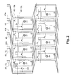
- Fig. 2 shows a possible example layout of pixels in an active matrix type organic EL display device wherein the delta arrangement is employed.
- the structure shown in Fig. 2 is designed so that the pixels of the same color which are connected to the same data line DL are symmetric about the data line DL.
- the first TFT 10 in a pixel for R ("R pixel") on the first row, the first TFT 10 is placed on the right side in the figure of the pixel and is connected to the data line 43r, and in an R pixel on the second row, the first TFT 10 is placed on the left side in the figure and is connected to the same data line 43r.
- the driving power supply line (VL) 45 is connected to a common driving power supply Pvdd and is not required to be connected to pixels of the same color. As described above, however, the driving power supply line VL 45 must not intersect the data line 43, in order to pattern the driving power supply line VL 45 simultaneously with the data line 43 using the same material. Therefore, the driving power supply line VL extending in the region between the R pixel and G pixel in the first row and connected to the second TFT 20 of the G pixel in the first row, as shown in Fig.
- the layout of Fig. 2 satisfies the conditions that the data line DL is connected to the pixels of the same color with a short wiring length and that the driving power supply line VL is connected to each pixel without intersecting the data line DL.
- the wiring undulates in a complex manner among the rows and the area occupied by the wiring in the region between the rows is large.
- the emission region formation region of the organic EL element
- improvements in aperture ratio cannot be achieved, that is, bright display cannot be produced.
- the total length of the wiring becomes long, and, consequently, the wiring resistance is also increased.
- the maximum current value that can be supplied by the driving power supply line 45 must be substantially the same for any pixel at any position of the display device, otherwise a variation in emission brightness will occur among the organic EL elements 50 on a display screen. Therefore, when the wiring resistance of the driving power supply line 45 is increased, there is a problem in that the pixels located at positions farther away from the driving power supply will exhibit lower emission brightness because of the voltage drop caused by the wiring resistance of the longer driving power supply line.
- the present invention was conceived to solve the problem described above, and an object of the present invention is to simplify the wiring pattern in an active matrix type display device utilizing an organic EL element or the like.
- an active matrix type display device comprising a plurality of pixels arranged in a matrix form, wherein each of the pixels comprises an element to be driven, an element driving thin film transistor for supplying power from a driving power supply line to the element to be driven, and a switching thin film transistor for controlling the element driving thin film transistor based on a data signal supplied from a data line when selected, and, in each pixel, of a first side and a second side of a pixel which opposes each other, the driving power supply line is placed on the second side, being the side opposite the data line, in a section where the switching thin film transistor is connected to the data line and is placed on the first side, which is the same side as the data line, in a section where the element driving thin film transistor is connected to the driving power supply line.
- the driving power supply line extends from the second side of the pixel across the pixel to the first side of the pixel through a region between the switching thin film transistor and the element to be driven within the pixel.
- the driving power supply line extends from the second side of the pixel through a region between the switching thin film transistor and the element to be driven within the pixel to the first side of the pixel in a direction along an extension direction of a selection line for supplying a selection signal to the switching thin film transistor.
- the driving power supply line As described above, it is possible to achieve a very simple wiring pattern between adjacent rows in a matrix without adversely affecting other circuit elements electrically due to the presence of the driving power supply line, such as, for example, generation of a parasitic capacitance.
- the driving power supply line crosses within the pixel region from the second side to the first side, by employing a pattern in which the driving power supply line extends through a region between the switching thin film transistor and the element to be driven in a direction, for example, along the extension direction of the selection line as described above, it is possible to eliminate a diagonally extending portion of a wiring which tends to reduce the wiring efficiency in a matrix arrangement. Therefore, it is possible to improve the wiring efficiency and to increase the emission region of the pixel.
- an active matrix type display device comprising a plurality of pixels arranged in a matrix form, wherein each of the pixels comprises an element to be driven, an element driving thin film transistor for supplying power from a driving power supply line to the element to be driven, and a switching thin film transistor for controlling the element driving thin film transistor based on a data signal supplied from a data line when selected, and in each pixel, a region of connection between the switching thin film transistor and the data line and a region of connection between the element driving thin film transistor and the driving power supply line are provided near a first side of the pixel.
- connection region between the data line and the switching thin film transistor can be provided, for example, on a second side of the pixel in order to prevent obstruction by the driving power supply line.
- the element driving thin film transistor formed on the first side can be connected to the driving power supply line extending across from the second side to the first side.
- an active matrix type display device comprising a plurality of pixels arranged in a matrix form, wherein each of the pixels comprises an element to be driven, an element driving thin film transistor for supplying power from a driving power supply line to the element to be driven, and a switching thin film transistor for controlling the element driving thin film transistor based on a data signal supplied from a data line when selected; a gate of the element driving thin film transistor is connected to a corresponding switching thin film transistor; and the driving power supply line extends, in each pixel, across the pixel and intersects a connection wiring path between the gate of the element driving thin film transistor and the switching thin film transistor.
- the driving power supply line is placed to extend across the pixel region, for example, when the connection wiring path is integral with the gate of the element driving thin film transistor, even if the driving power supply line crosses the wiring path, it is possible to form the gate and the driving power supply line using different materials through different steps as different layers so that the gate and the driving power supply line can be formed such that at least these layers are insulated. No special insulative structure is necessary for allowing these layers to intersect. Therefore, it is possible to accommodate the delta arrangement or the like while designing a driving power supply line of minimum wiring length.
- the plurality of pixels are arranged in the column direction of the matrix such that the pixels of the same color in adjacent rows are shifted from each other in the row direction.
- the data line extends in the column direction of the matrix through a region between each pixel, and the switching thin film transistors of the pixels of the same color which are provided alternately for each row on the left side of the data line and on the right side of the data line are connected to the data line.
- the driving power supply line extends in the column direction without intersecting the data line and is connected to the element driving thin film transistor of a corresponding pixel.
- wiring for a data line for supplying a data signal to each pixel and for a driving power supply line for supplying power to each pixel can be provided in a simple manner.
- the wiring pattern of the driving power supply line it is possible to minimize the wiring length similar to the data line and, thus, it is possible to maximize the emission region of each pixel and to realize bright, high resolution color display devices.
- Fig. 3 shows a pixel layout of an active matrix type EL display device having m rows and n columns according to an embodiment of the present invention.
- a pixel is represented in Fig. 3 by a region surrounded by one-dotted chain lines.
- the circuit structure is identical to that shown in Fig. 1 and each pixel comprises an organic EL element 50 as an element to be driven, a switching TFT (first TFT) 10, an element driving TFT (second TFT) 20, and a storage capacitor Cs.
- first TFT switching TFT
- second TFT element driving TFT
- the gate of the first TFT 10 is connected to a gate line (GL) 40.
- a drain of the first TFT 10 is connected to a data line (DL) 42 and a source is connected to the storage capacitor Cs.
- the storage capacitor Cs comprises a first electrode which is integral with the source of the first TFT 10 and a second electrode provided to oppose the first electrode.
- the second electrode is formed integral with a capacitance line (SL) 46 extending in the row direction.
- the source of the first TFT 10 and the first electrode of the storage capacitor Cs are connected to a gate of the second TFT 20.
- a source of the second TFT 20 is connected to a driving power supply line (VL) 44 and a drain is connected to an anode of the organic EL element 50.
- the conductivity of the first and second TFTs 10 and 20 are not limited to n-ch and p-ch as described above.
- conductivities for the TFTs may be reversed (p-ch for the first TFT 10 and n-ch for the second TFT 20) or the same conductivity may be employed for both TFTs (n-ch for both first and second TFTs 10 and 20 or p-ch for both first and second TFTs 10 and 20).
- the layouts for the data line 42 and the driving power supply line 44 are identical to the layouts which will be described below.
- a pixel has a circuit structure as described above .
- Each pixel corresponds to one color among R (red), G (green), and B (blue), and a delta arrangement is employed in which the pixels of the same color are aligned in the column direction and shifted by a predetermined pitch (in Fig. 3, a distance corresponding to slightly less than two pixels) for each row.
- the data line DL 42 is connected to the first TFTs 10 of the pixels of the same color which are shifted for each row and provided alternately on the right side and on the left side with respect to the data line 42.
- the data line 42 extends in the column direction while undulating between the pixels.
- a layout is employed in which the driving power supply line 44 extends in the column direction while crossing, in each pixel, the formation region of the pixel and is connected to the second TFT 20.
- the driving power supply line 44 supplies electric current to the organic EL element 50 through the second TFT 20.
- the driving power supply line 44 is placed on a second side (on the right side in Fig. 3) which opposes a side on which the data line for R pixel is placed (a first side; shown on the left side in Fig. 3) in a section where the first TFT 10 of the R pixel is connected to the data line 42R for R.
- the first and second TFTs 10 and 20 of each pixel are placed near the same side (in this example, the first side on which the data line is placed) of the opposing sides (first side and second side) along the column direction of thepixel. Therefore, the driving power supply line 44 extends across within the R pixel from the second side to the first side to which the data line 42 is placed in order to connect to the second TFT 20. In a section where the driving power supply line 44 is connected to the second TFT 20, the driving power supply line 44 is placed on the first side of the pixel and extends in the column direction while being aligned with the data line 42R for R.
- a driving power supply line 44 is placed on a second side (right side in Fig. 3) of the pixel opposite the data line 42G for G so that the driving power supply line 44 does not obstruct the connection.
- the driving power supply line 44 is placed on a first side (left side in Fig. 3) of the pixel which is the same side as the data line 42G for G.
- the second row will now be described referring to a G pixel under the R pixel of the first row as an example.
- the driving power supply line 44 extending in an approximate straight line in the column direction on the first side of the R pixel of the first row (right side in Fig. 3) is placed on a second side of the G pixel of the second row, that is, the side (on the left side of Fig. 3) opposite the first side of the G pixel of the second row on which the data line 42G for G is placed.
- the driving power supply line 44 extends across the G pixel region of the second row from the second side to the first side, and in a section of the G pixel where the second TFT 20 of the G pixel and the driving power supply line 44 are connected, the driving power supply line 44 is placed on the right side of Fig. 3 which is the first side of the G pixel and extends in the column direction while being aligned with the data line 42G (for G) placed also on the first side of the G pixel.
- the position of the region across which the driving power supply line 44 extends in each pixel be a position which does not affect the formation region of the organic EL element 50 which substantially defines the emission region in each pixel.
- the emission region in each pixel is substantially defined by the formation region of the organic EL element 50, in particular, by the extension region of the anode which is formed individually for each pixel.
- the first and second TFTs 10 and 20 for driving the organic EL element 50, the storage capacitor Cs, etc. are placed in the remaining region of each pixel and, thus, this remaining region does not contribute to light emission.
- the driving power supply line 44 extends from the second side of the pixel, across the pixel through a region between the first TFT 10 and the organic EL element 50 in the pixel along the extension direction of the gate line 40 to the first side of the pixel, and in the column direction on the first side while being aligned with the data line 42.
- the second TFT 20 supplies current from the driving power supply line 44 to the organic EL element 50
- the second TFT 20 is provided near the formation region of the organic EL element 50.
- the first TFT 10 which captures a data signal upon reception of a selection signal from the gate line 40 is provided near the gate line 40. Therefore, in order to place the driving power supply line 44 avoiding the formation region of the organic EL element 50 as much as possible and not intersecting the data line 42, it is desirable to place the driving power supply line 44 to pass through a region between the emission region (formation region of the organic EL element 50) and the formation region of the first TFT 10.
- the gate electrode of the second TFT 20 is electrically connected to a source (or drain) of the first TFT 10.
- the driving power supply line 44 which extends across the region between the organic EL element 50 and the first TFT 10 as described above intersects a wiring path between the gate of the second TFT 20 and the source of the first TFT 10.
- the driving power supply line 44 is arranged so that it does not intersect the data line 42.
- the driving power supply line 44 and the data line 42 are formed using the same material such as, for example, A1, through simultaneously patterning.
- the gate line 40, the storage capacitor line 46, and the gate electrode of the second TFT are formed using a material such as, for example, Cr, through simultaneous patterning of a layer below the layer of the driving power supply line 44 and the data line 42 with an interlayer insulative layer interposed therebetween. Therefore, even when the driving power supply line 44 extends across the pixel and intersects the gate of the second TFT 20 as described above, the driving power supply line 44 can be insulated from the gate of the second TFT 20 by the interlayer insulative layer, thus allowing for relatively free wiring pattern of the driving power supply line 44 above the gate electrode of the second TFT 20 or the wiring layer formed integral with the gate of the second TFT 20.
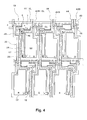
- Fig. 4 shows an example planer structure of a pixel corresponding to the circuit layout as described above.
- Figs. 5A and 5B respectively show cross sections along the A-A line of Fig. 4 (cross section of the first TFT) and along the B-B line of Fig. 4 (cross section of the second TFT) .
- a delta arrangement is employed in which the pixels of the same color are shifted for each row by a distance corresponding to approximately 1.5 pixels.
- an organic EL element 50, a first TFT 10, a second TFT 20, and a storage capacitor Cs for one pixel are formed in a region defined by gate lines 40 and data lines 42.
- the first TFT 10 is formed in a region near the intersection between the gate line GL and the data line DL.
- the first TFT 10 of each pixel in the first row is placed on the left side of the pixel (a first side of the pixel) while the first TFT 10 of each pixel in the second row is placed on the right side of the pixel (a first side of the pixel).
- an active layer 6 of the first TFT 10 is formed on a transparent insulative substrate 1 such as glass.
- the active layer 6 is made of p-Si produced by polycrystallizing a-Si through a laser annealing treatment.
- a gate electrode 2 integral with a gate line 40 is formed to protrude from the gate line 40.
- Two gate electrodes 2 are formed on a gate insulative film 4 formed to cover the active layer 6, to form a TFT having a double gate structure circuit-wise.
- a region beneath the gate electrode 2 is a channel region 6c, and a drain region 6d and a source region 6s to which an impurity such as phosphorus (P) is doped are provided in regions on both sides of the channel region 6c, to form an n-ch TFT.
- an impurity such as phosphorus (P)
- the drain region 6d of the first TFT 10 is connected to the data line 42 which is formed on an interlayer insulative film 14 formed to cover the entirety of the first TFT 10 and which supplies a data signal of a corresponding color to a pixel, through a contact hole provided in the interlayer insulative film 14 and in the gate insulative film 4.
- the storage capacitor Cs is connected to the source region 6s of the first TFT 10.
- the storage capacitor Cs is formed in a region where a first electrode 7 and a second electrode 8 overlap with the gate insulative film 4 interposed therebetween.
- the first electrode 7 extends in the row direction similar to the gate line 40 as shown in Fig. 4 and is formed integral with the capacitance line 46 formed using the same material as the gate.
- the second electrode 8 is integral with the active layer 6 of the first TFT 10 and is formed by the active layer 6 extending to the formation position of the first electrode 7. As shown in Fig. 4, the second electrode 8 is connected to a gate electrode 24 of the second TFT 20 through a connector 48 on the first side of the pixel which is the side on which the first and second TFTs 10 and 20 are placed.
- the second TFT 20 is formed, similar to the first TFT 10, within a pixel on the side on which the data line 42 for supplying a data signal to the pixel is placed.
- both the first TFT 10 and the second TFT 20 are placed on the first side on which the data line 42 is placed.
- the second TFT 20 has a cross sectional structure as shown in Fig. 5B, and, in the present embodiment, comprises an elongated channel 16c along the extension direction (column direction) of the data line 42.
- the active layer 16 of the second TFT 20 is formed on the substrate 1 simultaneously with the active layer 6 of the first TFT 10, and thus, polycrystalline silicon formed by polycrystalli zing a-Si through a laser annealing treatment is utilized.
- the channel length direction of the second TFT 20 is set to be along the longitudinal direction of the pixel having an elongated shape. It is not necessary, however, to set the channel length direction in this manner or to significantly elongate the channel length as shown in the drawings.
- a structure in which a sufficiently long channel length is secured in the direction along the extension direction of the data line in the case where a pulse-shaped laser is scanned in the channel length direction, for example, polycrystallization of the entire region of the active layer of the second TFT 20 cannot be achieved by one pulse and, thus, this structure necessitates polycrystallization through a plurality of laser irradiation pulses. With such a structure, it is possible to prevent significant differences to be created in the transistor characteristics among the second TFTs 20 of pixels in different positions.
- a gate insulative film 4 is formed on the active layer 16 made of a polycrystalline silicon and, similar to the first TFT 10, a gate electrode 24 of the second TFT 20 is formed on the gate insulative film 4.
- the gate electrode 24 of the second TFT 20 is connected through a connector 48 to the second electrode 8 of the storage capacitor Cs which is integral with the active layer 6 of the first TFT 10 and is patterned to extend from the connector 48 placed on the end of the first side of the pixel to widely cover, on the gate insulative film 4, a region above the active layer 16.
- a channel region 16c is formed in the region covered by the gate electrode 24, and a source region 16s and a drain region 16d are respectively formed on both sides of the channel region 16c.
- the source region 16s of the active layer 16 is connected to the driving power supply line 44 through a contact hole formed to penetrate through the gate insulative film 4 and the interlayer insulative film 14 over the active layer 16 on the first side of the pixel (in Fig. 4, the first side of the pixel and between the connector 48 and the organic EL element 50).
- the driving power supply line 44 is placed on the second side of the pixel in the section of the pixel where the first TFT 10 is connected to the data line 42, but in the positions below the section of the pixel where the second TFT 20 is connected to the driving power supply line 44 (downward direction in Fig. 4), the driving power supply line 44 extends in the column direction on the first side of the pixel while being aligned with the data line 42.
- the driving power supply line 44 extends in the column direction on the first side of the pixel while being aligned with the data line 42.
- the driving power supply line 44 extends in the row direction across the pixel from the second side through a region between the storage capacitor Cs and the organic EL element 50 to the first side, is connected to the active layer 16 of the second TFT 20, and extends in the column direction substantially parallel to the data line 42 for supplying a data signal to the pixel of the second row.
- the shapes and structures of the first TFT 10 and second TFT 20 are not limited to those shown in Figs. 4, 5A, and 5B, but it is necessary that at least the contact position between the first TFT 10 and the data line 42 and the contact position between the second TFT 20 and the driving power supply line 44 are placed on the same side (for example, first side) of the pixel in order to simplify the wiring pattern of the driving power supply line 44.
- the connector 48 is placed between the data line 42 and the connection position between the active layer 16 and the driving power supply line 44 in a manner to avoid the driving power supply line 44.
- the connector 48 can be formed through patterning which is simultaneous with that of the data line 42 and the driving power supply line 44 using the same material such as, for example, Al.
- the connector 48 is placed to bypass in the row direction the contact between the driving power supply line 44 and the active layer 16.
- each pixel has an overall shape of approximate rectangle or a shape similar to a rectangle, although the center in the row direction of the formation region of the first TFT 10 and the storage capacitor Cs is slightly shifted with respect to that of the formation region of the second TFT 20 and the organic EL element 50.
- the overall shape is not limited to an approximate rectangular or a shape similar to a rectangle, but it is desirable to employ a structure in which the first TFT 10 and the second TFT 20 are placed on the side of the pixel through which the data line passes and the driving power supply line VL partially passes through the same side.
- the drain region 16d of the second TFT 20 is connected to a connector 26 near the gate line 40 corresponding to the next row in the matrix through a contact hole formed to penetrate through the gate insulative film 4 and the interlayer insulative film 14, wherein the connector 26 is formed simultaneously with the driving power supply line 44 or the like using the same material.
- the connector 26 extends from the contact position with the active layer 16 toward a formation region of an anode of the organic EL element 50 to be described below.
- the connector 26 is electrically connected to an anode 52 of the organic EL element 50 through a contact hole provided in a first planarization insulative layer 18 formed over the entire surface of the substrate covering the driving power supply line 44, data line 42, and connectors 48 and 26.
- a second planarization insulative layer 61 is formed on the first planarization insulative layer 18, the second planarization insulative layer 61 having an opening only in the central region of formation of the anode 52 of the organic EL element 50 and covering the edge of the anode 52, the wiring region, and the formation region of the first and second TFTs.
- a light emitting element layer 51 of the organic EL element 50 is formed on the anode 52 and the second planarization insulative layer 61.
- a metal electrode 57 which is common to all pixels is formed above the light emitting element layer 51.
- the organic EL element 50 comprises a transparent anode 52 made of a material such as ITO (Indium Tin Oxide), a cathode 57 made of a metal such as, for example, A1, and a light emitting element layer (organic layer) 51 between the anode 52 and the cathode 57 in which organic compounds are used.
- a transparent anode 52 made of a material such as ITO (Indium Tin Oxide)
- a cathode 57 made of a metal such as, for example, A1
- a light emitting element layer (organic layer) 51 between the anode 52 and the cathode 57 in which organic compounds are used.
- the anode 52, light emitting element layer 51, and cathode 57 are layered in that order from the side of the substrate 1.
- the light emitting element layer 51 in this example structure comprises, for example, a hole transport layer 54, an organic emissive layer 55, and an electron transport layer 56 layered from the anode through, for example, vacuum evaporation.
- At least the emissive layer 55 is made of a material different for each emission color, but the hole transport layer 54 and the electron transport layer 56 may be formed to be common for all pixels as shown in Figs. 5A and 5B. Examples of materials that may be used for each layer are listed below.
- the hole transport layer may further comprise a first hole transport layer and a second hole transport layer which are made of different materials.
- Each light emitting element layer 51 comprises at least an emissive layer 55 which contains an emissive material, but the hole transport layer and the electron transport layer may not be necessary depending on the materials to be used.
- the unabbreviated names for the above abbreviated materials are as follows. The present invention is not limited to the exemplified configuration.
- NBP N,N'-di((naphthalene-1-yl)-N,N'-diphenyl-benzidine)
- ACJTB (2-(1,1-dimethylethyl)-6-(2-(2,3,6,7-tetrahydro-1,1,7,7-tetram ethyl-1H,5H-benzo[ij]quinolizin-9-yl)ethenyl)-4H-pyran-4-ylide ne)propanedinitrile
- coumarin 6 3-(2-benzothiazolyl)-7-(diethylamino)coumarin
- the present invention thus allows an approximate rectangular shape for each pixel, in particular, for the formation region of the organic EL element 50.
- the bend in the shape of the pixel becomes more significant to a shape of ">" or " ⁇ ", thus causing the pattern of the formation region of the organic EL element to be similarly bent.
- the light emitting element layer 51 is formed through vacuum evaporation.
- evaporation (deposition) layer of individual pattern for each pixel it is necessary to perform the evaporation while placing, between a substrate and an evaporation source, an evaporation mask having one or a plurality of openings corresponding to the pattern.
- an organic layer is patterned through the openings formed on the evaporation mask as described, it may be more difficult to uniformly evaporate through a complicated opening pattern having a large bend than through a simple rectangular opening pattern. Therefore, by planning the layout of each element in a pixel and wiring pattern of the driving power supply line 44 as in the present embodiment, it is also possible to more uniformly form the organic layer (evaporation layer) of the organic EL element 50.
Landscapes
- Engineering & Computer Science (AREA)
- Physics & Mathematics (AREA)
- Computer Hardware Design (AREA)
- General Physics & Mathematics (AREA)
- Theoretical Computer Science (AREA)
- Microelectronics & Electronic Packaging (AREA)
- Devices For Indicating Variable Information By Combining Individual Elements (AREA)
- Electroluminescent Light Sources (AREA)
- Control Of Indicators Other Than Cathode Ray Tubes (AREA)
- Control Of El Displays (AREA)
- Liquid Crystal (AREA)
Abstract
Description
"NBP" N,N'-di((naphthalene-1-yl)-N,N'-diphenyl-benzidine)
"Alq3" tris(8-hydroxyquinolinato)aluminum
"DCJTB"
(2-(1,1-dimethylethyl)-6-(2-(2,3,6,7-tetrahydro-1,1,7,7-tetram ethyl-1H,5H-benzo[ij]quinolizin-9-yl)ethenyl)-4H-pyran-4-ylide ne)propanedinitrile
"
Claims (8)
- An active matrix type display device comprising a plurality of pixels arranged in a matrix form, wherein
each of said pixels comprises an element to be driven, an element driving thin film transistor for supplying power from a driving power supply line to said element to be driven, and a switching thin film transistor for controlling said element driving thin film transistor based on a data signal supplied from a data line when selected, and
in each pixel, of a first side and a second side of the pixel which oppose each other, said driving power supply line is placed on said second side, being the side opposite said data line, in a section where said switching thin film transistor is connected to said data line, and said driving power supply line is placed on said first side which is the same side as said data line in a section where said element driving thin film transistor is connected to said driving power supply line. - An active matrix type display device according to claim 1, wherein
said driving power supply line extends from said second side of the pixel across the pixel to said first side of the pixel through a region between said switching thin film transistor and said element to be driven within the pixel. - An active matrix type display device according to claim 1, wherein
said driving power supply line extends from said second side of the pixel through a region between said switching thin film transistor and said element to be driven within the pixel to said first side of the pixel in a direction along the extension direction of a selection line for supplying a selection signal to said switching thin film transistor. - An active matrix type display device comprising a plurality of pixels arranged in a matrix form, wherein
each of said pixels comprises an element to be driven, an element driving thin film transistor for supplying power from a driving power supply line to said element to be driven, and a switching thin film transistor for controlling said element driving thin film transistor based on a data signal supplied from a data line when selected, and
in each pixel, a region of connection between said switching thin film transistor and said data line and a region of connection between said element driving thin film transistor and said driving power supply line are placed near a first side of the pixel. - An active matrix type display device comprising a plurality of pixels arranged in a matrix form, wherein
each of said pixels comprises an element to be driven, an element driving thin film transistor for supplying power from a driving power supply line to said element to be driven, and a switching thin film transistor for controlling said element driving thin film transistor based on a data signal supplied from a data line when selected;
a gate of said element driving thin film transistor is connected to a corresponding switching thin film transistor; and
said driving power supply line extends, in each pixel, across the pixel and intersects a connection wiring path between the gate of said element driving thin film transistor and said switching thin film transistor. - An active matrix type display device according to any one of claims 1 through 5, wherein
said plurality of pixels are arranged in the column direction of said matrix such that the pixels of the same color in adjacent rows are shifted from each other in the row direction. - An active matrix type display device according to claim 6, wherein
said data line extends in the column direction of said matrix through a region between each pixel, and
said switching thin film transistors of the pixels of the same color which are provided alternately for each row on the left side of said data line and on the right side of said data line are connected to said data line. - An active matrix type display device according to either claim 6 or 7, wherein
said driving power supply line extends in the column direction without intersecting said data line and is connected to said element driving thin film transistor of a corresponding pixel.
Applications Claiming Priority (2)
| Application Number | Priority Date | Filing Date | Title |
|---|---|---|---|
| JP2001303788 | 2001-09-28 | ||
| JP2001303788A JP4380954B2 (en) | 2001-09-28 | 2001-09-28 | Active matrix display device |
Publications (2)
| Publication Number | Publication Date |
|---|---|
| EP1298634A2 true EP1298634A2 (en) | 2003-04-02 |
| EP1298634A3 EP1298634A3 (en) | 2007-04-11 |
Family
ID=19123821
Family Applications (1)
| Application Number | Title | Priority Date | Filing Date |
|---|---|---|---|
| EP02256758A Withdrawn EP1298634A3 (en) | 2001-09-28 | 2002-09-27 | Active matrix type display device |
Country Status (6)
| Country | Link |
|---|---|
| US (1) | US6847343B2 (en) |
| EP (1) | EP1298634A3 (en) |
| JP (1) | JP4380954B2 (en) |
| KR (1) | KR100493353B1 (en) |
| CN (1) | CN1251165C (en) |
| TW (1) | TW546601B (en) |
Cited By (5)
| Publication number | Priority date | Publication date | Assignee | Title |
|---|---|---|---|---|
| EP1473778A1 (en) | 2003-04-29 | 2004-11-03 | Samsung SDI Co., Ltd. | Flat panel display |
| US8866707B2 (en) | 2005-03-31 | 2014-10-21 | Semiconductor Energy Laboratory Co., Ltd. | Display device, and apparatus using the display device having a polygonal pixel electrode |
| US9423657B2 (en) | 2007-12-03 | 2016-08-23 | Semiconductor Energy Laboratory Co., Ltd. | TFT arrangement for display device |
| EP3537480A1 (en) * | 2018-03-09 | 2019-09-11 | Samsung Display Co., Ltd. | Display apparatus |
| US11552107B2 (en) | 2015-12-11 | 2023-01-10 | Semiconductor Energy Laboratory Co., Ltd. | Display device |
Families Citing this family (47)
| Publication number | Priority date | Publication date | Assignee | Title |
|---|---|---|---|---|
| KR100637433B1 (en) | 2004-05-24 | 2006-10-20 | 삼성에스디아이 주식회사 | Light emitting display |
| JP4122949B2 (en) * | 2002-11-29 | 2008-07-23 | セイコーエプソン株式会社 | Electro-optical device, active matrix substrate, and electronic apparatus |
| JP4488709B2 (en) * | 2003-09-29 | 2010-06-23 | 三洋電機株式会社 | Organic EL panel |
| JP4443179B2 (en) * | 2003-09-29 | 2010-03-31 | 三洋電機株式会社 | Organic EL panel |
| JP4446707B2 (en) * | 2003-09-30 | 2010-04-07 | 三洋電機株式会社 | Active matrix display device |
| KR100741961B1 (en) | 2003-11-25 | 2007-07-23 | 삼성에스디아이 주식회사 | Flat panel display and its driving method |
| JP4686122B2 (en) * | 2003-11-28 | 2011-05-18 | 東芝モバイルディスプレイ株式会社 | Active matrix display device and manufacturing method thereof |
| KR101026812B1 (en) * | 2003-11-28 | 2011-04-04 | 삼성전자주식회사 | Thin film transistor array panel and manufacturing method thereof |
| JP3985788B2 (en) * | 2004-01-22 | 2007-10-03 | セイコーエプソン株式会社 | Electro-optical device and electronic apparatus |
| US20050231447A1 (en) * | 2004-04-14 | 2005-10-20 | Shuo-Hsiu Hu | Pixel arrangement in a display system |
| JP2005352147A (en) * | 2004-06-10 | 2005-12-22 | Tohoku Pioneer Corp | Active matrix light-emitting display panel |
| KR100636503B1 (en) * | 2004-06-25 | 2006-10-18 | 삼성에스디아이 주식회사 | Light emitting display device and manufacturing method thereof |
| JP4846998B2 (en) * | 2004-10-08 | 2011-12-28 | 株式会社 日立ディスプレイズ | Image display device |
| KR100612392B1 (en) | 2004-10-13 | 2006-08-16 | 삼성에스디아이 주식회사 | Light emitting display device and light emitting display panel |
| KR100688802B1 (en) | 2004-11-22 | 2007-03-02 | 삼성에스디아이 주식회사 | Pixel and light emitting display |
| KR100688801B1 (en) | 2004-11-22 | 2007-03-02 | 삼성에스디아이 주식회사 | Delta pixel circuit and light emitting display |
| US7382384B2 (en) | 2004-12-07 | 2008-06-03 | Eastman Kodak Company | OLED displays with varying sized pixels |
| KR100698697B1 (en) * | 2004-12-09 | 2007-03-23 | 삼성에스디아이 주식회사 | Light emitting display device and manufacturing method thereof |
| US7868883B2 (en) * | 2005-05-27 | 2011-01-11 | Seiko Epson Corporation | Electro-optical device and electronic apparatus having the same |
| JP2007103584A (en) | 2005-10-03 | 2007-04-19 | Ricoh Co Ltd | Transistor element, display device, and manufacturing method thereof |
| US8026669B2 (en) | 2006-03-31 | 2011-09-27 | Canon Kabushiki Kaisha | Display device |
| JP5309468B2 (en) * | 2006-05-31 | 2013-10-09 | 株式会社ニコン | Liquid crystal display element, display device, observation device, and camera |
| JP5109302B2 (en) * | 2006-07-31 | 2012-12-26 | ソニー株式会社 | Display device and manufacturing method thereof |
| US8654045B2 (en) | 2006-07-31 | 2014-02-18 | Sony Corporation | Display and method for manufacturing display |
| US7507998B2 (en) * | 2006-09-29 | 2009-03-24 | Tpo Displays Corp. | System for displaying images and method for fabricating the same |
| JP4600420B2 (en) * | 2007-04-20 | 2010-12-15 | セイコーエプソン株式会社 | Electro-optical device and electronic apparatus |
| JP4600419B2 (en) * | 2007-04-20 | 2010-12-15 | セイコーエプソン株式会社 | Electro-optical device and electronic apparatus |
| JP4655061B2 (en) * | 2007-04-20 | 2011-03-23 | セイコーエプソン株式会社 | Electro-optical device and electronic apparatus |
| JP5056265B2 (en) | 2007-08-15 | 2012-10-24 | ソニー株式会社 | Display device and electronic device |
| JP2009116206A (en) * | 2007-11-09 | 2009-05-28 | Sony Corp | El display panel and electronic device |
| JP5245879B2 (en) | 2008-03-26 | 2013-07-24 | ソニー株式会社 | Image display device and method of repairing short circuit accident |
| TWI453910B (en) | 2009-02-04 | 2014-09-21 | 新力股份有限公司 | Image display device and repair method of short circuit accident |
| WO2010139175A1 (en) * | 2009-06-05 | 2010-12-09 | 北京维信诺科技有限公司 | Organic electroluminescence device and testing method thereof |
| WO2011057461A1 (en) | 2009-11-13 | 2011-05-19 | 北京维信诺科技有限公司 | Organic materials and organic electroluminescent apparatuses using the same |
| JP2011243441A (en) * | 2010-05-19 | 2011-12-01 | Nec Lighting Ltd | Organic el device |
| KR102061791B1 (en) * | 2012-11-13 | 2020-01-03 | 삼성디스플레이 주식회사 | Organinc light emitting display device and manufacturing method for the same |
| TWI518657B (en) | 2014-03-31 | 2016-01-21 | 友達光電股份有限公司 | Pixel element of organic electroluminescent display |
| JP2016075868A (en) * | 2014-10-09 | 2016-05-12 | Nltテクノロジー株式会社 | Pixel array, electro-optical device, electric apparatus, and pixel rendering method |
| KR102357345B1 (en) * | 2015-01-27 | 2022-02-03 | 삼성디스플레이 주식회사 | Organic light emitting display device |
| CN106531043B (en) * | 2015-09-11 | 2019-07-23 | 群创光电股份有限公司 | Display device |
| CN105116579B (en) * | 2015-09-30 | 2019-05-03 | 深圳市华星光电技术有限公司 | Liquid crystal display panel and driving method thereof |
| KR102528296B1 (en) * | 2015-11-18 | 2023-05-04 | 삼성디스플레이 주식회사 | Ddisplay apparatus |
| US10224386B2 (en) * | 2016-09-23 | 2019-03-05 | Apple Inc. | Display with power supply mesh |
| WO2019187047A1 (en) * | 2018-03-30 | 2019-10-03 | シャープ株式会社 | Display device |
| WO2020065992A1 (en) * | 2018-09-28 | 2020-04-02 | シャープ株式会社 | Display device |
| CN116075772B (en) * | 2021-08-30 | 2026-01-13 | 京东方科技集团股份有限公司 | Display substrate and display device |
| CN116193933B (en) * | 2023-03-14 | 2025-10-21 | 武汉天马微电子有限公司 | Display panel and display device |
Family Cites Families (15)
| Publication number | Priority date | Publication date | Assignee | Title |
|---|---|---|---|---|
| US5822026A (en) * | 1994-02-17 | 1998-10-13 | Seiko Epson Corporation | Active matrix substrate and color liquid crystal display |
| JP3256110B2 (en) * | 1995-09-28 | 2002-02-12 | シャープ株式会社 | Liquid crystal display |
| JP3069280B2 (en) * | 1995-12-12 | 2000-07-24 | 松下電器産業株式会社 | Active matrix type liquid crystal display device and driving method thereof |
| JP3541625B2 (en) * | 1997-07-02 | 2004-07-14 | セイコーエプソン株式会社 | Display device and active matrix substrate |
| US7119870B1 (en) * | 1998-11-27 | 2006-10-10 | Sanyo Electric Co., Ltd. | Liquid crystal display device having particular drain lines and orientation control window |
| JP2000227770A (en) * | 1998-12-01 | 2000-08-15 | Sanyo Electric Co Ltd | Color EL display device |
| JP2000221524A (en) * | 1999-01-29 | 2000-08-11 | Sanyo Electric Co Ltd | Color liquid crystal display |
| US6724149B2 (en) * | 1999-02-24 | 2004-04-20 | Sanyo Electric Co., Ltd. | Emissive display device and electroluminescence display device with uniform luminance |
| JP4497596B2 (en) * | 1999-09-30 | 2010-07-07 | 三洋電機株式会社 | Thin film transistor and display device |
| JP3710969B2 (en) * | 1999-09-30 | 2005-10-26 | 三洋電機株式会社 | Electroluminescence display device |
| JP2001109395A (en) * | 1999-10-01 | 2001-04-20 | Sanyo Electric Co Ltd | EL display device |
| JP4596582B2 (en) * | 1999-11-05 | 2010-12-08 | 三洋電機株式会社 | Display device |
| JP3736399B2 (en) * | 2000-09-20 | 2006-01-18 | セイコーエプソン株式会社 | Drive circuit for active matrix display device, electronic apparatus, drive method for electro-optical device, and electro-optical device |
| JP4925528B2 (en) * | 2000-09-29 | 2012-04-25 | 三洋電機株式会社 | Display device |
| JP2002251167A (en) * | 2001-02-26 | 2002-09-06 | Sanyo Electric Co Ltd | Display device |
-
2001
- 2001-09-28 JP JP2001303788A patent/JP4380954B2/en not_active Expired - Lifetime
-
2002
- 2002-09-19 TW TW091121441A patent/TW546601B/en not_active IP Right Cessation
- 2002-09-26 CN CNB02143381XA patent/CN1251165C/en not_active Expired - Lifetime
- 2002-09-27 EP EP02256758A patent/EP1298634A3/en not_active Withdrawn
- 2002-09-27 US US10/256,313 patent/US6847343B2/en not_active Expired - Lifetime
- 2002-09-28 KR KR10-2002-0059091A patent/KR100493353B1/en not_active Expired - Lifetime
Cited By (10)
| Publication number | Priority date | Publication date | Assignee | Title |
|---|---|---|---|---|
| EP1473778A1 (en) | 2003-04-29 | 2004-11-03 | Samsung SDI Co., Ltd. | Flat panel display |
| US7196747B2 (en) | 2003-04-29 | 2007-03-27 | Samsung Sdi Co., Ltd. | Flat panel display comprising semiconductor layer with heterogeous lines |
| US8866707B2 (en) | 2005-03-31 | 2014-10-21 | Semiconductor Energy Laboratory Co., Ltd. | Display device, and apparatus using the display device having a polygonal pixel electrode |
| US9423657B2 (en) | 2007-12-03 | 2016-08-23 | Semiconductor Energy Laboratory Co., Ltd. | TFT arrangement for display device |
| US11552107B2 (en) | 2015-12-11 | 2023-01-10 | Semiconductor Energy Laboratory Co., Ltd. | Display device |
| US11881489B2 (en) | 2015-12-11 | 2024-01-23 | Semiconductor Energy Laboratory Co., Ltd. | Display device |
| US12170291B2 (en) | 2015-12-11 | 2024-12-17 | Semiconductor Energy Laboratory Co., Ltd. | Display device |
| EP3537480A1 (en) * | 2018-03-09 | 2019-09-11 | Samsung Display Co., Ltd. | Display apparatus |
| US11600679B2 (en) | 2018-03-09 | 2023-03-07 | Samsung Display Co., Ltd. | Display apparatus |
| US12256614B2 (en) | 2018-03-09 | 2025-03-18 | Samsung Display Co., Ltd. | Display apparatus |
Also Published As
| Publication number | Publication date |
|---|---|
| TW546601B (en) | 2003-08-11 |
| CN1251165C (en) | 2006-04-12 |
| KR20030027858A (en) | 2003-04-07 |
| KR100493353B1 (en) | 2005-06-07 |
| CN1410962A (en) | 2003-04-16 |
| US6847343B2 (en) | 2005-01-25 |
| JP4380954B2 (en) | 2009-12-09 |
| EP1298634A3 (en) | 2007-04-11 |
| US20030067458A1 (en) | 2003-04-10 |
| JP2003108032A (en) | 2003-04-11 |
Similar Documents
| Publication | Publication Date | Title |
|---|---|---|
| US6847343B2 (en) | Active matrix type display device | |
| EP1655781B1 (en) | Flat panel display | |
| EP0935229B1 (en) | Display | |
| KR100488835B1 (en) | Semiconductor device and display device | |
| US8022900B2 (en) | OLED display | |
| US7683382B2 (en) | Organic light emitting diode display | |
| US7724216B2 (en) | Display panel | |
| US20040196220A1 (en) | Light-emitting apparatus and method of manufacturing light-emitting apparatus | |
| US20070096135A1 (en) | Display panel | |
| US7671366B2 (en) | Thin film transistor and organic light emitting device including thin film transistor | |
| US7742023B2 (en) | Electroluminescence display device | |
| US8013523B2 (en) | Organic light emitting device and manufacturing method thereof | |
| KR100689913B1 (en) | Active matrix display | |
| KR101100885B1 (en) | Thin film transistor array panel for organic light emitting display | |
| KR102691133B1 (en) | TFT substrate and light emitting display device including the same | |
| US20120169699A1 (en) | Organic luminescent display device and method of manufacturing the same | |
| KR20040078560A (en) | Electro luminescence display device | |
| KR100911205B1 (en) | Active matrix display | |
| JP2004004192A (en) | Display | |
| KR20080008772A (en) | Organic light emitting display |
Legal Events
| Date | Code | Title | Description |
|---|---|---|---|
| PUAI | Public reference made under article 153(3) epc to a published international application that has entered the european phase |
Free format text: ORIGINAL CODE: 0009012 |
|
| AK | Designated contracting states |
Kind code of ref document: A2 Designated state(s): AT BE BG CH CY CZ DE DK EE ES FI FR GB GR IE IT LI LU MC NL PT SE SK TR Designated state(s): AT BE BG CH CY CZ DE DK EE ES FI FR GB GR IE IT LI LU MC NL PT SE SK TR |
|
| AX | Request for extension of the european patent |
Extension state: AL LT LV MK RO SI |
|
| PUAL | Search report despatched |
Free format text: ORIGINAL CODE: 0009013 |
|
| STAA | Information on the status of an ep patent application or granted ep patent |
Free format text: STATUS: THE APPLICATION HAS BEEN WITHDRAWN |
|
| AK | Designated contracting states |
Kind code of ref document: A3 Designated state(s): AT BE BG CH CY CZ DE DK EE ES FI FR GB GR IE IT LI LU MC NL PT SE SK TR |
|
| AX | Request for extension of the european patent |
Extension state: AL LT LV MK RO SI |
|
| 18W | Application withdrawn |
Effective date: 20070305 |