EP1298583A1 - Image processing system - Google Patents
Image processing system Download PDFInfo
- Publication number
- EP1298583A1 EP1298583A1 EP01936847A EP01936847A EP1298583A1 EP 1298583 A1 EP1298583 A1 EP 1298583A1 EP 01936847 A EP01936847 A EP 01936847A EP 01936847 A EP01936847 A EP 01936847A EP 1298583 A1 EP1298583 A1 EP 1298583A1
- Authority
- EP
- European Patent Office
- Prior art keywords
- image
- defects
- image processing
- host computer
- processing
- Prior art date
- Legal status (The legal status is an assumption and is not a legal conclusion. Google has not performed a legal analysis and makes no representation as to the accuracy of the status listed.)
- Withdrawn
Links
Images


Classifications
-
- G—PHYSICS
- G06—COMPUTING OR CALCULATING; COUNTING
- G06T—IMAGE DATA PROCESSING OR GENERATION, IN GENERAL
- G06T1/00—General purpose image data processing
-
- G—PHYSICS
- G06—COMPUTING OR CALCULATING; COUNTING
- G06T—IMAGE DATA PROCESSING OR GENERATION, IN GENERAL
- G06T7/00—Image analysis
- G06T7/0002—Inspection of images, e.g. flaw detection
- G06T7/0004—Industrial image inspection
-
- G—PHYSICS
- G06—COMPUTING OR CALCULATING; COUNTING
- G06T—IMAGE DATA PROCESSING OR GENERATION, IN GENERAL
- G06T1/00—General purpose image data processing
- G06T1/0007—Image acquisition
Definitions
- a lighting device for example, a fluorescent lamp
- a light beam from the lighting device 28 passes through the glass substrate 26, and then, enters a light receiving portion (i.e., a sensor) of each of the line sensor cameras 32-1 to 32-4.
- the line sensor camera receives an image of an object to be inspected, and then, outputs image data.
- the board computer is provided with an image input board having the functions of inputting the image data and performing a part of image processing, in one-to-one correspondence to the line sensor camera.
- the computer subjects the image data transmitted from the line sensor camera via the image input board to the image processing, so as to obtain and classify information data on defects of the object to be inspected.
- a recent personal computer can perform all the processing of image data transmitted from line sensor cameras by the use of its own software owing to its enhanced processing ability and a bulk memory mounted thereon, without using any hardware specifically designed for image processing.
- the amount of data which a single computer system can process at real time is not more than the amount of image data transmitted from a single line sensor camera having a sensor of 10,000 pixels under the current circumstances.
- one computer is assigned to one line sensor camera in processing the image data transmitted from a plurality of line sensor cameras, and thus, a plurality of computers perform the image processing.
- the result of the image processing is transferred to an independent host computer connected via a high-speed network. Thereafter, the host computer receives the results of the image processing transmitted from the computers, and finally, displays the result of all of the image processing on a display device.
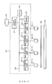
- Fig. 2 is a diagram illustrating the configuration of a mode carrying out an image processing system according to the present invention.
Landscapes
- Engineering & Computer Science (AREA)
- Physics & Mathematics (AREA)
- General Physics & Mathematics (AREA)
- Theoretical Computer Science (AREA)
- Quality & Reliability (AREA)
- Computer Vision & Pattern Recognition (AREA)
- Investigating Materials By The Use Of Optical Means Adapted For Particular Applications (AREA)
- Image Processing (AREA)
- Image Analysis (AREA)
- Facsimiles In General (AREA)
Abstract
Description
Claims (10)
- An image processing system comprising:a plurality of image input means, each of which receives an image of an object to be inspected, and then, outputs image data;a plurality of computers provided with image input boards, each of which does not perform any image processing but has only the function of inputting the image data, in one-to-one correspondence to the image input means, the computer subjecting the image data transmitted from the image input means via the image input board to the image processing, so as to obtain and classify information data on defects of the object to be inspected;a host computer connected to the computers via a network, so as to process the classified information data on the defects, transferred from the computers; anddisplay means for displaying the result of the processing by the host computer.
- An image processing system as claimed in claim 1, wherein the host computer subjects the classified information data on the defects, transferred from the computers to sorting processing, so as to judge whether or not there are the predetermined number or more of defects, each having a predetermined size or larger.
- An image processing system as claimed in claim 1, wherein the host computer performs a part of the processing of obtaining and classifying the information data on the defects of the object to be inspected, the processing being performed by the computer.
- An image processing system as claimed in claim 1, wherein the computers are provided with the plurality of image input boards, so as to perform the image processing of the image data transmitted from the plurality of image input means, thus obtaining the information data on the defects of the object to be inspected.
- An image processing system as claimed in claim 1, wherein the image processing includes the processing of expressing the image data at a predetermined slice level in a binary form, and subsequently, labeling the data.
- An image processing system comprising:a plurality of image input means, each of which receives an image of an object to be inspected, and then, outputs image data;a plurality of computers provided with image input boards, each having the functions of inputting the image data and performing a part of image processing, in one-to-one correspondence to the image input means, the computer subjecting the image data transmitted from the image input means via the image input board to the image processing, so as to obtain and classify information data on defects of the object to be inspected;a host computer connected to the computers via a network, so as to process the classified information data on the defects, transferred from the computers; anddisplay means for displaying the result of the processing by the host computer.
- An image processing system as claimed in claim 6, wherein the host computer subjects the classified information data on the defects, transferred from the computers to sorting processing, so as to judge whether or not there are the predetermined number or more of defects, each having a predetermined size or larger.
- An image processing system as claimed in claim 6, wherein the host computer performs a part of the processing of obtaining and classifying the information data on the defects of the object to be inspected, the processing being performed by the computer.
- An image processing system as claimed in claim 6, wherein the computers are provided with the plurality of image input boards, so as to perform the image processing of the image data transmitted from the plurality of image input means, thus obtaining the information data on the defects of the object to be inspected.
- An image processing system as claimed in claim 6, wherein the image processing includes the processing of expressing the image data at a predetermined slice level in a binary form, and subsequently, labeling the data.
Applications Claiming Priority (3)
| Application Number | Priority Date | Filing Date | Title |
|---|---|---|---|
| JP2000201906 | 2000-07-04 | ||
| JP2000201906A JP2002024802A (en) | 2000-07-04 | 2000-07-04 | Image processing system |
| PCT/JP2001/004722 WO2002003329A1 (en) | 2000-07-04 | 2001-06-05 | Image processing system |
Publications (2)
| Publication Number | Publication Date |
|---|---|
| EP1298583A1 true EP1298583A1 (en) | 2003-04-02 |
| EP1298583A4 EP1298583A4 (en) | 2006-11-29 |
Family
ID=18699509
Family Applications (1)
| Application Number | Title | Priority Date | Filing Date |
|---|---|---|---|
| EP01936847A Withdrawn EP1298583A4 (en) | 2000-07-04 | 2001-06-05 | Image processing system |
Country Status (7)
| Country | Link |
|---|---|
| US (1) | US20030122731A1 (en) |
| EP (1) | EP1298583A4 (en) |
| JP (1) | JP2002024802A (en) |
| KR (1) | KR20030013520A (en) |
| CN (1) | CN1418352A (en) |
| TW (1) | TWI268452B (en) |
| WO (1) | WO2002003329A1 (en) |
Families Citing this family (11)
| Publication number | Priority date | Publication date | Assignee | Title |
|---|---|---|---|---|
| US20050058350A1 (en) * | 2003-09-15 | 2005-03-17 | Lockheed Martin Corporation | System and method for object identification |
| KR100525312B1 (en) * | 2003-11-28 | 2005-11-23 | 삼성코닝정밀유리 주식회사 | Method for measuring particles of a glass substrate |
| CN101581677B (en) * | 2008-05-16 | 2012-10-03 | 深超光电(深圳)有限公司 | Method for classifying grade of panel to be detected of lighting tester |
| KR100903184B1 (en) * | 2008-06-17 | 2009-06-17 | (주)이즈미디어 | Cellular multi-camera device |
| JP5189570B2 (en) * | 2009-08-19 | 2013-04-24 | 株式会社キーエンス | Image processing apparatus and image processing method |
| US9955123B2 (en) | 2012-03-02 | 2018-04-24 | Sight Machine, Inc. | Machine-vision system and method for remote quality inspection of a product |
| US20230068903A1 (en) * | 2012-05-18 | 2023-03-02 | View, Inc. | Mitigating defects using polygon ablation pattern |
| CN102980893A (en) * | 2012-11-13 | 2013-03-20 | 上海交通大学 | Classification detection system and method of ingot surface defect |
| CN108508023B (en) * | 2018-03-30 | 2021-06-04 | 苏州阚创检测有限公司 | Defect detection system for contact end jacking bolt in railway contact network |
| JP7270361B2 (en) * | 2018-10-12 | 2023-05-10 | Ckd株式会社 | Inspection equipment remote response system |
| CN116684744A (en) * | 2023-05-19 | 2023-09-01 | 广东科技学院 | A Machine Vision Recognition and Classification System |
Family Cites Families (14)
| Publication number | Priority date | Publication date | Assignee | Title |
|---|---|---|---|---|
| JPS6051980A (en) * | 1983-08-31 | 1985-03-23 | Toshiba Corp | On-line pattern recognizing device |
| JPH0713838B2 (en) * | 1984-11-16 | 1995-02-15 | 三菱電機株式会社 | Item inspection method |
| JPH0358289A (en) * | 1989-07-27 | 1991-03-13 | Mitsubishi Electric Corp | Picture processor |
| JPH03188358A (en) * | 1989-12-19 | 1991-08-16 | Hajime Sangyo Kk | Apparatus for inspecting surface of body |
| US5440648A (en) * | 1991-11-19 | 1995-08-08 | Dalsa, Inc. | High speed defect detection apparatus having defect detection circuits mounted in the camera housing |
| JPH06341960A (en) * | 1993-05-31 | 1994-12-13 | Nippon Avionics Co Ltd | Image processing method/device for pattern |
| CA2142224A1 (en) * | 1994-02-28 | 1995-08-29 | Ronald S. Cok | Real-time demand-driven imaging architecture |
| JPH0829357A (en) * | 1994-07-13 | 1996-02-02 | Meidensha Corp | Automated line visual inspection device |
| JPH0944634A (en) * | 1995-07-28 | 1997-02-14 | Canon Inc | Video input device |
| JPH09138200A (en) * | 1995-11-14 | 1997-05-27 | Nkk Corp | Method for determining surface defects on strips |
| JPH10293848A (en) * | 1997-04-21 | 1998-11-04 | Fuji Electric Co Ltd | Parallel processing unit for image data |
| US6020957A (en) * | 1998-04-30 | 2000-02-01 | Kla-Tencor Corporation | System and method for inspecting semiconductor wafers |
| US6778695B1 (en) * | 1999-12-23 | 2004-08-17 | Franklin M. Schellenberg | Design-based reticle defect prioritization |
| US6831998B1 (en) * | 2000-06-22 | 2004-12-14 | Hitachi, Ltd. | Inspection system for circuit patterns and a method thereof |
-
2000
- 2000-07-04 JP JP2000201906A patent/JP2002024802A/en active Pending
-
2001
- 2001-06-05 EP EP01936847A patent/EP1298583A4/en not_active Withdrawn
- 2001-06-05 KR KR10-2003-7000061A patent/KR20030013520A/en not_active Ceased
- 2001-06-05 WO PCT/JP2001/004722 patent/WO2002003329A1/en not_active Ceased
- 2001-06-05 CN CN01806762A patent/CN1418352A/en active Pending
- 2001-06-05 US US10/239,012 patent/US20030122731A1/en not_active Abandoned
- 2001-06-26 TW TW090115382A patent/TWI268452B/en active
Also Published As
| Publication number | Publication date |
|---|---|
| JP2002024802A (en) | 2002-01-25 |
| EP1298583A4 (en) | 2006-11-29 |
| WO2002003329A1 (en) | 2002-01-10 |
| CN1418352A (en) | 2003-05-14 |
| TWI268452B (en) | 2006-12-11 |
| KR20030013520A (en) | 2003-02-14 |
| US20030122731A1 (en) | 2003-07-03 |
Similar Documents
| Publication | Publication Date | Title |
|---|---|---|
| KR102378186B1 (en) | Artificial intelligence vision inspection system for wiring harness | |
| US20030122731A1 (en) | Image processing system | |
| AU4773500A (en) | Pixel classification in object inspection based on likelihood | |
| CN110018172A (en) | Product inspection system and method | |
| CN111551559A (en) | LCD (liquid Crystal display) liquid crystal screen defect detection method based on multi-view vision system | |
| CN114926464B (en) | Image quality inspection method, image quality inspection device and system in double-recording scene | |
| CN115019160A (en) | Intelligent control method for warehouse-in logistics of factory warehouse | |
| KR102286470B1 (en) | LED Digital Signage Defect Detection system through Similarity Analysis of Original Image Information and Displayed Image Information | |
| EP0460431B1 (en) | A method of and an equipment for optical inspection of strip and sheet products | |
| JP2000172844A (en) | Print inspection method and print inspection device | |
| CN110502966B (en) | Package classification information acquisition equipment, method and storage device | |
| CN111681228A (en) | Flaw detection model, training method, detection method, apparatus, device, and medium | |
| JP2003262593A (en) | Defect detection device and defect detection method | |
| CN108346132B (en) | Certificate imaging method and device, camera device and certificate imaging system | |
| JP4212904B2 (en) | Method and apparatus for detecting pinhole defects and dirt defects on a transparent body | |
| CN110969177A (en) | A prepackage quality identification method based on deep learning | |
| JP2002319021A (en) | Binarization processing method, appearance inspection method, and appearance inspection device | |
| JP2001209793A (en) | Pattern defect detection method | |
| JP2002298144A (en) | Automatic target detection identification processing method, device, program, recording medium, and visible camera device | |
| JP3278518B2 (en) | Method and apparatus for detecting structural and / or pattern defects of an object | |
| EP4443142A1 (en) | Car body inspection device, car body inspection system, and car body inspection method | |
| JPH03160309A (en) | Image quality testing apparatus | |
| CN116071356B (en) | Intelligent inspection platform and inspection method for defects of design drawing of design enterprise | |
| CN115376121A (en) | Image recognition method and device, electronic equipment and readable storage medium | |
| JP2001116653A (en) | Method and apparatus for evaluating screen display characteristics |
Legal Events
| Date | Code | Title | Description |
|---|---|---|---|
| PUAI | Public reference made under article 153(3) epc to a published international application that has entered the european phase |
Free format text: ORIGINAL CODE: 0009012 |
|
| 17P | Request for examination filed |
Effective date: 20020911 |
|
| AK | Designated contracting states |
Kind code of ref document: A1 Designated state(s): AT BE CH CY DE DK ES FI FR GB GR IE IT LI LU MC NL PT SE TR Designated state(s): AT BE CH CY DE DK ES FI FR GB GR IE IT LI LU MC NL PT SE TR |
|
| RBV | Designated contracting states (corrected) |
Designated state(s): AT BE CH CY DE FR GB IT LI |
|
| A4 | Supplementary search report drawn up and despatched |
Effective date: 20061102 |
|
| 17Q | First examination report despatched |
Effective date: 20070308 |
|
| STAA | Information on the status of an ep patent application or granted ep patent |
Free format text: STATUS: THE APPLICATION IS DEEMED TO BE WITHDRAWN |
|
| 18D | Application deemed to be withdrawn |
Effective date: 20070719 |