EP1297617B1 - Frequency modulator using a pll - Google Patents
Frequency modulator using a pll Download PDFInfo
- Publication number
- EP1297617B1 EP1297617B1 EP01940864A EP01940864A EP1297617B1 EP 1297617 B1 EP1297617 B1 EP 1297617B1 EP 01940864 A EP01940864 A EP 01940864A EP 01940864 A EP01940864 A EP 01940864A EP 1297617 B1 EP1297617 B1 EP 1297617B1
- Authority
- EP
- European Patent Office
- Prior art keywords
- tuning
- voltage
- control voltage
- controlled oscillator
- vco
- Prior art date
- Legal status (The legal status is an assumption and is not a legal conclusion. Google has not performed a legal analysis and makes no representation as to the accuracy of the status listed.)
- Expired - Lifetime
Links
- 230000007423 decrease Effects 0.000 claims description 4
- 239000003990 capacitor Substances 0.000 description 11
- 230000035945 sensitivity Effects 0.000 description 9
- 238000000034 method Methods 0.000 description 3
- 230000000295 complement effect Effects 0.000 description 1
- 238000007796 conventional method Methods 0.000 description 1
- 230000005236 sound signal Effects 0.000 description 1
- 230000006641 stabilisation Effects 0.000 description 1
- 238000011105 stabilization Methods 0.000 description 1
Images


Classifications
-
- H—ELECTRICITY
- H03—ELECTRONIC CIRCUITRY
- H03L—AUTOMATIC CONTROL, STARTING, SYNCHRONISATION OR STABILISATION OF GENERATORS OF ELECTRONIC OSCILLATIONS OR PULSES
- H03L7/00—Automatic control of frequency or phase; Synchronisation
- H03L7/06—Automatic control of frequency or phase; Synchronisation using a reference signal applied to a frequency- or phase-locked loop
- H03L7/08—Details of the phase-locked loop
- H03L7/099—Details of the phase-locked loop concerning mainly the controlled oscillator of the loop
-
- H—ELECTRICITY
- H03—ELECTRONIC CIRCUITRY
- H03B—GENERATION OF OSCILLATIONS, DIRECTLY OR BY FREQUENCY-CHANGING, BY CIRCUITS EMPLOYING ACTIVE ELEMENTS WHICH OPERATE IN A NON-SWITCHING MANNER; GENERATION OF NOISE BY SUCH CIRCUITS
- H03B5/00—Generation of oscillations using amplifier with regenerative feedback from output to input
- H03B5/18—Generation of oscillations using amplifier with regenerative feedback from output to input with frequency-determining element comprising distributed inductance and capacitance
- H03B5/1841—Generation of oscillations using amplifier with regenerative feedback from output to input with frequency-determining element comprising distributed inductance and capacitance the frequency-determining element being a strip line resonator
-
- H—ELECTRICITY
- H03—ELECTRONIC CIRCUITRY
- H03L—AUTOMATIC CONTROL, STARTING, SYNCHRONISATION OR STABILISATION OF GENERATORS OF ELECTRONIC OSCILLATIONS OR PULSES
- H03L7/00—Automatic control of frequency or phase; Synchronisation
- H03L7/06—Automatic control of frequency or phase; Synchronisation using a reference signal applied to a frequency- or phase-locked loop
- H03L7/16—Indirect frequency synthesis, i.e. generating a desired one of a number of predetermined frequencies using a frequency- or phase-locked loop
- H03L7/18—Indirect frequency synthesis, i.e. generating a desired one of a number of predetermined frequencies using a frequency- or phase-locked loop using a frequency divider or counter in the loop
- H03L7/183—Indirect frequency synthesis, i.e. generating a desired one of a number of predetermined frequencies using a frequency- or phase-locked loop using a frequency divider or counter in the loop a time difference being used for locking the loop, the counter counting between fixed numbers or the frequency divider dividing by a fixed number
- H03L7/187—Indirect frequency synthesis, i.e. generating a desired one of a number of predetermined frequencies using a frequency- or phase-locked loop using a frequency divider or counter in the loop a time difference being used for locking the loop, the counter counting between fixed numbers or the frequency divider dividing by a fixed number using means for coarse tuning the voltage controlled oscillator of the loop
- H03L7/189—Indirect frequency synthesis, i.e. generating a desired one of a number of predetermined frequencies using a frequency- or phase-locked loop using a frequency divider or counter in the loop a time difference being used for locking the loop, the counter counting between fixed numbers or the frequency divider dividing by a fixed number using means for coarse tuning the voltage controlled oscillator of the loop comprising a D/A converter for generating a coarse tuning voltage
-
- H—ELECTRICITY
- H03—ELECTRONIC CIRCUITRY
- H03L—AUTOMATIC CONTROL, STARTING, SYNCHRONISATION OR STABILISATION OF GENERATORS OF ELECTRONIC OSCILLATIONS OR PULSES
- H03L2207/00—Indexing scheme relating to automatic control of frequency or phase and to synchronisation
- H03L2207/06—Phase locked loops with a controlled oscillator having at least two frequency control terminals
Definitions
- the present invention relates to tunable phase locked loop systems in general, and to systems which include a voltage controlled oscillator, in particular.
- Frequency synthesizer phase locked loops are widely used in communication transceivers. These loops typically include a voltage-controlled oscillator (VCO).
- VCO voltage-controlled oscillator
- variables voltage controlled capacitors
- the varactor has significantly non-linear response to applied voltage, especially at low voltages. Such a behavior leads to the use of high varactor control voltages, typically 12 Volts or more, to achieve the VCO tuning range that is needed for feedback transceiver applications.
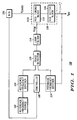
- Frequency synthesizer 100 includes a reference frequency source 102, a reference frequency divider 104, a digital-to-analog converter (DAC) 106, a controller 108, a phase detector 110, a loop filter 118, a VCO 120 and a feedback frequency divider 114.
- VCO 120 further includes a VCO tuning block 112 and a VCO active block 116.
- Reference frequency divider 104 is coupled to reference frequency source 102, controller 108 and phase detector 110.
- Feedback frequency divider 114 is coupled to phase detector 110, controller 108 and VCO active block 116.
- Loop filter 118 is coupled to phase detector 110 and to VCO tuning block 112.
- DAC 106 is coupled to VCO tuning block 112 and to controller 108.
- VCO active block 116 is coupled to VCO tuning block 112 and to feedback frequency divider 114.
- Reference frequency divider 104 receives a signal, having the frequency F R , from frequency source 102. Reference frequency divider 104 further divides this signal by N and provides the resultant signal, having the frequency F R /N, to phase detector 110.
- Feedback frequency divider 114 receives a feedback signal, having the output frequency F OUT , from VCO active block 116. Feedback frequency divider 114 further divides this signal by M and provides the resultant signal, having the frequency F OUT /M, to phase detector 110.
- Phase detector 110 compares these two signals, generates a respective output control signal and provides it to loop filter 118.
- loop filter 118 is a low-pass filter. It integrates the output control signal and provides the resultant output voltage V FINE to VCO tuning block 112.
- VCO tuning block 112 adjusts the output frequency F OUT so that it would be equal to the desired value M N ⁇ F R . This adjustment is performed within a comparatively narrow frequency range (fine-tuning). For a coarse tuning within a wide frequency range, DAC 106 provides a respective control signal V COARSE to VCO tuning block 112.
- VCO tuning block 112 includes two inductors 150 and 152, a first varactor VR C 158, a second varactor VR F 160, three capacitors 154, 156 and 164 and a resonator 162.
- Varactor VR C 158 is coupled to inductor 150 and capacitor 154.
- Varactor VR F 160 is coupled to inductance 152 and capacitor 156.
- Resonator 162 is coupled to capacitors 154, 156 and 164.
- a varactor is a voltage-controlled diode whose capacitance changes with applied voltage. The character of this change is non-linear.
- FIG. 3 is a graphical illustration of a typical dependence of varactor capacitance on applied voltage.
- the capacitance is maximal (for example, between 15 pF and 25 pF) and at high voltages (for example between 3.5 Volts and 4.5 Volts) the capacitance is minimal (for example, between 2 pF and 3 pF).
- Varactor voltage sensitivity which is a derivative of varactor capacitance with respect to applied voltage, also changes in a non-linear manner. The voltage sensitivity of the varactor is much higher for the lower values of applied voltage than for the higher values of applied voltage.
- the capacitance of varactor VR C 158 is controlled by the voltage provided by DAC 106 of Figure 1 via inductor 150. This steering voltage is responsible for a coarse tuning.
- the capacitance of varactor VR F 160 is controlled by the output voltage V FINE , provided by loop filter 118 of Figure 1 .
- the output voltage V FINE is provided to varactor 160 via inductor 152.
- the output control signal executes a fine tuning of the VCO. Since a VCO operating frequency is inversely proportional to the varactor capacitance, VCO sensitivity is much greater at low operating frequencies than at high operating frequencies. In order to increase the operating frequency range while keeping the VCO sensitivity at a low level, known devices use comparatively high voltages for VCO tuning (up to 13 Volts).
- New generations of IC for portable communication devices are based on low-voltage elements (3 - 5 Volts maximum). According to the foregoing explanation, variations of the control voltage within 5 Volts range will lead to a reduction of the operation frequency bandwidth and to large variations of the VCO gain. It is therefore desirable to have a low-voltage VCO circuit with varactors, which will provide the required operating frequency range and low VCO sensitivity.
- Prior art published United Kingdom patent application GB-A-2,338,128 shows a voltage controlled oscillator.
- GB-A-2,338,128 describes a method for flattening the frequency modulation deviation over the frequency range of the VCO. This invention can be used in radio transmitters that use FM modulation and directly modulate the VCO.
- Prior art published United States patent US-A-4,003,004 is concerned with getting a linear response to the FM modulating signal from the VCO.
- the modulation signal goes through modulation FET amplifier 50 to the varactors 30/32, thus FM modulating the VCO.
- FET amplifier response is compensating for varactor nonlinearity and the response to the modulation signal is linear.
- US-A-4,904,964 describes a VCO wherein a control voltage is utilised for modulation compensation by a modulation compensation network.
- the method described in US-A-4,904,964 is aimed at use in a frequency modulated transmitter wherein an audio signal modulates the VCO.
- the method allows FM deviation to be flattened over the frequency range of the VCO.
- a resonator of the VCO is described which includes a varactor whose cathode is connected to a control voltage input obtained from a phase locked loop.
- the invention now to be described is not disclosed or suggested in US-A-4,904,964 .
- VCO voltage-controlled oscillator
- VCO voltage controlled oscillator
- the VCO circuit according to the invention may include a voltage source for applying to the second tuning element a voltage which opposes the external control voltage applied thereto whereby when the external control voltage increases the overall voltage across the second tuning element decreases.
- the tuning parameter of each of the tuning elements is desirably a capacitance, the capacitance of each tuning element varying within a predetermined range in response to a control voltage applied thereto.
- the capacitance of each of said tuning elements may depend non-linearly on the respective control voltage applied across the element.
- the tuning elements are preferable varactors.
- a phase locked loop (PLL) circuit for a frequency synthesizer includes a VCO circuit according to first aspect and a phase detector for comparing a phase of a reference signal with a phase of an output VCO signal from the VCO circuit, the phase detector generating an output signal for a fine VCO tuning, the output signal being responsive to the difference between the phases of the reference signal and the output VCO signal, the PLL further including a controller, and a control voltage source, the controller being coupled to the input of the control voltage source, the control voltage source generating a control voltage for the coarse VCO tuning at the output, the control voltage being responsive to commands from the controller.
- PLL phase locked loop
- the present invention mitigates the disadvantages of the prior art by providing a tunable VCO, which requires low control voltage values to provide a wide-band control range.
- VCO tuning block 200 includes four inductors 202, 204, 206 and 224, seven capacitors 210, 212, 216, 218, 220, 226 and 230, a first varactor VR C 208, a second varactor VR 1 214, a third varactor VR F 222, and a resonator 228.
- Varactor VR C 208 is coupled to inductor 202 and capacitor 210.
- Varactor VR 1 214 is coupled to inductors 204 and 206 and to capacitors 212 and 216.
- Varactor VR F 222 is coupled to inductor 224 and to capacitors 220 and 226.
- Capacitor 218 is coupled to capacitors 220, 230, 212 and 210, and to resonator 228.
- Inductor 206 is coupled to inductor 202.
- DAC 106 of Figure 1 provides V COARSE voltage to varactor VR C 208, via inductor 202, and to varactor VR 1 214 via inductor 206.
- additional bias voltage for example, +5V
- varactor VR 1 214 changes with the applied voltage V COARSE in a manner, which is opposite to that of varactor VR C 208.
- FIG. 5 is a graphical illustration of a typical dependence of the capacitance of varactor VR 1 214 of Figure 4 on applied voltage.
- the capacitance of varactor VR 1 214 as well as its sensitivity, are minimal for low V COARSE values and maximal for high V COARSE values.
- the capacitance of varactor VR C 208 is high and the capacitance of varactor VR 1 214 is low when V COARSE is low.
- the capacitance of varactor VR C 208 is low and the capacitance of varactor VR 1 214 is high.
- the resulting change of the capacitance, as well as that of the VCO sensitivity, over the entire range of V COARSE variations is small. This allows applying comparatively low voltages (up to 5 Volts) for controlling VCO operating frequency over a wide frequency range, while keeping low VCO sensitivity.
- the present invention provides the possibility of designing a wideband VCO, while keeping the VCO gain constant and small.
- the present invention is not intended to be used for flattening the FM deviation, as was the arrangement of GB-A-2338128 .
- Vsteer in GB-A-2338128 corresponds to Vfine in the present invention. This is the line that is connected to the Loop Filter, and via this line, the phase locked loop is steering the VCO.
- the purpose of the present invention is to make the VCO sensitivity to this steering line as small as desired, and constant across the VCO frequency band.
- the purpose of GB-A-2338128 is to keep the VCO response to the audio modulation signal flat over the VCO frequency range.
- GB-A-2338128 does not keep VCO gain (dF/dVsteer) low and constant.
- Vcoarse in the present invention is controlling the VCO banding, and, at the same time, contributes to VCO gain flatness via the VR1 arrangement.
- Vcoarse is a DC voltage.
- the VR1 (214) arrangement allows the present invention to get complementary varactor response as shown in figure 5 of the appended drawings.
- the present invention is completely different from GB-A-2338128 , both in it's objectives and in how the invention works.
- the present invention differs from the arrangement of US 4,003,004 .
- the present invention achieves small and constant VCO gain over the VCO frequency range.
- the objective of the present invention is therefore different from US 4,003,004 .
Landscapes
- Stabilization Of Oscillater, Synchronisation, Frequency Synthesizers (AREA)
- Oscillators With Electromechanical Resonators (AREA)
- Amplifiers (AREA)
- Inductance-Capacitance Distribution Constants And Capacitance-Resistance Oscillators (AREA)
- Digital Transmission Methods That Use Modulated Carrier Waves (AREA)
- Optical Communication System (AREA)
Abstract
Description
- The present invention relates to tunable phase locked loop systems in general, and to systems which include a voltage controlled oscillator, in particular.
- Frequency synthesizer phase locked loops are widely used in communication transceivers. These loops typically include a voltage-controlled oscillator (VCO). In these conventional techniques, voltage controlled capacitors (varactors), are usually used to vary the resonant frequency of the VCO tuning network in accordance with a control voltage. The varactor has significantly non-linear response to applied voltage, especially at low voltages. Such a behavior leads to the use of high varactor control voltages, typically 12 Volts or more, to achieve the VCO tuning range that is needed for feedback transceiver applications.
- Reference is now made to
Figure 1 , which is a schematic illustration of a conventional phase locked loop frequency synthesizer, generally referenced 100.Frequency synthesizer 100 includes areference frequency source 102, areference frequency divider 104, a digital-to-analog converter (DAC) 106, acontroller 108, aphase detector 110, aloop filter 118, aVCO 120 and afeedback frequency divider 114. VCO 120 further includes aVCO tuning block 112 and a VCOactive block 116. -
Reference frequency divider 104 is coupled toreference frequency source 102,controller 108 andphase detector 110.Feedback frequency divider 114 is coupled tophase detector 110,controller 108 and VCOactive block 116.Loop filter 118 is coupled tophase detector 110 and toVCO tuning block 112.DAC 106 is coupled toVCO tuning block 112 and to controller 108. VCOactive block 116 is coupled toVCO tuning block 112 and tofeedback frequency divider 114. -
Reference frequency divider 104 receives a signal, having the frequency FR, fromfrequency source 102.Reference frequency divider 104 further divides this signal by N and provides the resultant signal, having the frequency FR/N, tophase detector 110.Feedback frequency divider 114 receives a feedback signal, having the output frequency FOUT, from VCOactive block 116.Feedback frequency divider 114 further divides this signal by M and provides the resultant signal, having the frequency FOUT/M, tophase detector 110.Phase detector 110 compares these two signals, generates a respective output control signal and provides it to loopfilter 118. Typically,loop filter 118 is a low-pass filter. It integrates the output control signal and provides the resultant output voltage VFINE toVCO tuning block 112. Depending on the value of VFINE,VCO tuning block 112 adjusts the output frequency FOUT so that it would be equal to the desired value
DAC 106 provides a respective control signal VCOARSE toVCO tuning block 112. - Reference is now made to
Figure 2 , which is a schematic illustration in detail of a conventionalVCO tuning block 112 ofFigure 1 .VCO tuning block 112 includes twoinductors first varactor VR C 158, asecond varactor VR F 160, threecapacitors resonator 162. -
Varactor VR C 158 is coupled toinductor 150 andcapacitor 154. VaractorVR F 160 is coupled toinductance 152 andcapacitor 156.Resonator 162 is coupled tocapacitors - A varactor is a voltage-controlled diode whose capacitance changes with applied voltage. The character of this change is non-linear.
- Reference is now made to
Figure 3 , which is a graphical illustration of a typical dependence of varactor capacitance on applied voltage. At low voltages (for example, between 0.5 Volts and 1.5 Volts) the capacitance is maximal (for example, between 15 pF and 25 pF) and at high voltages (for example between 3.5 Volts and 4.5 Volts) the capacitance is minimal (for example, between 2 pF and 3 pF). Varactor voltage sensitivity, which is a derivative of varactor capacitance with respect to applied voltage, also changes in a non-linear manner. The voltage sensitivity of the varactor is much higher for the lower values of applied voltage than for the higher values of applied voltage. - Referring back to
Figure 2 , the capacitance ofvaractor VR C 158 is controlled by the voltage provided byDAC 106 ofFigure 1 viainductor 150. This steering voltage is responsible for a coarse tuning. The capacitance ofvaractor VR F 160 is controlled by the output voltage VFINE, provided byloop filter 118 ofFigure 1 . The output voltage VFINE is provided tovaractor 160 viainductor 152. The output control signal executes a fine tuning of the VCO. Since a VCO operating frequency is inversely proportional to the varactor capacitance, VCO sensitivity is much greater at low operating frequencies than at high operating frequencies. In order to increase the operating frequency range while keeping the VCO sensitivity at a low level, known devices use comparatively high voltages for VCO tuning (up to 13 Volts). - New generations of IC for portable communication devices are based on low-voltage elements (3 - 5 Volts maximum). According to the foregoing explanation, variations of the control voltage within 5 Volts range will lead to a reduction of the operation frequency bandwidth and to large variations of the VCO gain. It is therefore desirable to have a low-voltage VCO circuit with varactors, which will provide the required operating frequency range and low VCO sensitivity.
- Prior art published
United Kingdom patent application GB-A-2,338,128 GB-A-2,338,128 - Prior art published
United States patent US-A-4,003,004 is concerned with getting a linear response to the FM modulating signal from the VCO. Referring tofigure 1 , the modulation signal goes through modulation FET amplifier 50 to the varactors 30/32, thus FM modulating the VCO. FET amplifier response is compensating for varactor nonlinearity and the response to the modulation signal is linear. -
US-A-4,904,964 describes a VCO wherein a control voltage is utilised for modulation compensation by a modulation compensation network. The method described inUS-A-4,904,964 is aimed at use in a frequency modulated transmitter wherein an audio signal modulates the VCO. The method allows FM deviation to be flattened over the frequency range of the VCO. InUS-A-4,904,964 a resonator of the VCO is described which includes a varactor whose cathode is connected to a control voltage input obtained from a phase locked loop. The invention now to be described is not disclosed or suggested inUS-A-4,904,964 . - It is an object of the present invention to provide a novel system, which includes voltage-controlled oscillator (VCO) with low-voltage gain stabilization, which mitigates the disadvantages of the prior art.
- It is another object of the present invention to provide a VCO with small gain variations in response to variations of the control voltage for coarse tuning.
- In accordance with the present invention in a first aspect , there is thus provided a voltage controlled oscillator (VCO) circuit as defined in
claim 1 of the accompanying claims. - The VCO circuit according to the invention may include a voltage source for applying to the second tuning element a voltage which opposes the external control voltage applied thereto whereby when the external control voltage increases the overall voltage across the second tuning element decreases.
- The tuning parameter of each of the tuning elements is desirably a capacitance, the capacitance of each tuning element varying within a predetermined range in response to a control voltage applied thereto. The capacitance of each of said tuning elements may depend non-linearly on the respective control voltage applied across the element. The tuning elements are preferable varactors.
- According to the present invention in a second aspect a phase locked loop (PLL) circuit for a frequency synthesizer includes a VCO circuit according to first aspect and a phase detector for comparing a phase of a reference signal with a phase of an output VCO signal from the VCO circuit, the phase detector generating an output signal for a fine VCO tuning, the output signal being responsive to the difference between the phases of the reference signal and the output VCO signal, the PLL further including a controller, and a control voltage source, the controller being coupled to the input of the control voltage source, the control voltage source generating a control voltage for the coarse VCO tuning at the output, the control voltage being responsive to commands from the controller.
- Embodiments of the present invention will now be described with reference to the accompanying drawings, in which:
- The present invention will be understood and appreciated more fully from the following detailed description taken in conjunction with the drawings in which:
-
Figure 1 is a schematic illustration of a prior art phase locked loop frequency synthesizer; -
Figure 2 is a schematic illustration in detail of VCO tuning block ofFigure 1 ; -
Figure 3 is a graphical illustration of a prior art typical dependence of varactor capacitance on applied voltage; -
Figure 4 is a schematic illustration of a VCO tuning block, constructed and operative in accordance with a preferred embodiment of the present invention; and -
Figure 5 is a graphical illustration of a typical dependence of the capacitance ofvaractor VR 1 214 ofFigure 4 on applied voltage. - The present invention mitigates the disadvantages of the prior art by providing a tunable VCO, which requires low control voltage values to provide a wide-band control range.
- Reference is now made to
Figure 4 , which is a schematic illustration of a VCO tuning block, generally referenced 200, constructed and operative in accordance with a preferred embodiment of the present invention.VCO tuning block 200 includes fourinductors capacitors first varactor VR C 208, asecond varactor VR 1 214, athird varactor VR F 222, and aresonator 228. -
Varactor VR C 208 is coupled toinductor 202 andcapacitor 210.Varactor VR 1 214 is coupled toinductors capacitors Varactor VR F 222 is coupled toinductor 224 and tocapacitors Capacitor 218 is coupled tocapacitors resonator 228.Inductor 206 is coupled toinductor 202. -
DAC 106 ofFigure 1 provides VCOARSE voltage to varactorVR C 208, viainductor 202, and to varactorVR 1 214 viainductor 206. According a to preferred embodiment of the present invention, additional bias voltage (for example, +5V) is applied tovaractor VR 1 214. In this case the capacitance ofvaractor VR 1 214 changes with the applied voltage VCOARSE in a manner, which is opposite to that ofvaractor VR C 208. - Reference is now made to
Figure 5 , which is a graphical illustration of a typical dependence of the capacitance ofvaractor VR 1 214 ofFigure 4 on applied voltage. In contrast to the dependence, which was presented inFigure 3 , the capacitance ofvaractor VR 1 214, as well as its sensitivity, are minimal for low VCOARSE values and maximal for high VCOARSE values. - Referring back to
Figure 4 , the capacitance ofvaractor VR C 208 is high and the capacitance ofvaractor VR 1 214 is low when VCOARSE is low. In an opposite case where the value of VCOARSE is high, then, the capacitance ofvaractor VR C 208 is low and the capacitance ofvaractor VR 1 214 is high. Thus, the resulting change of the capacitance, as well as that of the VCO sensitivity, over the entire range of VCOARSE variations, is small. This allows applying comparatively low voltages (up to 5 Volts) for controlling VCO operating frequency over a wide frequency range, while keeping low VCO sensitivity. - Returning now to a consideration of the prior art documents cited earlier, it is notable that the present invention provides the possibility of designing a wideband VCO, while keeping the VCO gain constant and small. The present invention is not intended to be used for flattening the FM deviation, as was the arrangement of
GB-A-2338128 - Here, reference is made to
Figure 4 inGB-A-2338128 Figure 4 in the present invention. Vsteer inGB-A-2338128 GB-A-2338128 GB-A-2338128 figure 5 of the appended drawings. In summary, the present invention is completely different fromGB-A-2338128 - The present invention differs from the arrangement of
US 4,003,004 . The present invention achieves small and constant VCO gain over the VCO frequency range. The objective of the present invention is therefore different fromUS 4,003,004 . - It will be appreciated by persons skilled in the art that the present invention is not limited to what has been particularly shown and described hereinabove. The scope of the present invention is defined only by the appended claims.
Claims (7)
- A voltage controlled oscillator circuit (200) comprising:a resonator (228);a plurality of tuning elements (208, 214) coupled in parallel to said resonator;a plurality of input ports (106, 118), each one of the tuning elements being coupled to a selected one of said input ports, each said input port being arranged to receive in operation a predetermined external control voltage;wherein each of said tuning elements comprises a voltage controlled device which varies a tuning parameter of the resonator;wherein a first tuning element (208) is arranged such that the tuning parameter provided thereby decreases with increasing applied external control voltage and a second tuning element (214) is arranged such that the tuning parameter provided thereby increases with increasing applied external control voltage,and characterised in that the first tuning element (208) and the second tuning element (214) are coupled to a first (106) of the input ports to receive a coarse control voltage (VCOARSE) from the first input port and the circuit (200) includes a third tuning element (222) coupled in parallel with the first tuning element and the second tuning element to the resonator, the third tuning element comprising a voltage controlled device which varies a tuning parameter of the resonator, the third tuning element being coupled to a second (118) of the input ports to receive a fine control voltage from the second input port.
- A voltage controlled oscillator circuit according to claim 1 wherein the third tuning element is operable such that a tuning parameter provided thereby decreases with increasing applied external control voltage
- A voltage controlled oscillator circuit according to claim 1 or claim 2 and including a voltage source (+5V) for applying to the second tuning element a voltage which opposes the external control voltage applied thereto whereby when the external control voltage increases the overall voltage across the second tuning element decreases.
- A voltage controlled oscillator circuit according to any one of claims 1 to 3, wherein the tuning parameter of each of the tuning elemnts is a capacitance, the capacitance of each tuning element varying within a predetermined range in response to a control voltage applied thereto.
- A voltage controlled oscillator circuit according to claim 4, wherein the capacitance of each of said tuning elements depends non-linearly with the respective control voltage applied across the element.
- A voltage controlled oscillator circuit according to claim 4 or claim 5, wherein the tuning elements are varactors.
- A phase locked loop circuit for a frequency synthesizer, the phase locked loop circuit including a voltage controlled oscillator circuit according to any one of the preceding claims and a phase detector for comparing a phase of a reference signal with a phase of an output signal from the voltage cotrolled oscillator circuit, the phase detector being operable to generate an output voltage signal for a fine tuning of the voltage controlled oscillator circuit, the output voltage signal being responsive to the difference between the phases of the reference signal and the output signal, the phase locked loop circuit further including a controller and a control voltage source, the controller being coupled to the input of the control voltage source, the control voltage source generating a control voltage for coarse tuning of the voltage controlled oscillator circuit, the control voltage being responsive to commands from the controller.
Applications Claiming Priority (3)
| Application Number | Priority Date | Filing Date | Title |
|---|---|---|---|
| GB0008695 | 2000-04-07 | ||
| GB0008695A GB2361122B (en) | 2000-04-07 | 2000-04-07 | VCO with low-voltage gain stabilization |
| PCT/IB2001/000593 WO2001078227A2 (en) | 2000-04-07 | 2001-04-09 | Frequency modulator using a pll |
Publications (2)
| Publication Number | Publication Date |
|---|---|
| EP1297617A2 EP1297617A2 (en) | 2003-04-02 |
| EP1297617B1 true EP1297617B1 (en) | 2008-03-19 |
Family
ID=9889517
Family Applications (1)
| Application Number | Title | Priority Date | Filing Date |
|---|---|---|---|
| EP01940864A Expired - Lifetime EP1297617B1 (en) | 2000-04-07 | 2001-04-09 | Frequency modulator using a pll |
Country Status (6)
| Country | Link |
|---|---|
| EP (1) | EP1297617B1 (en) |
| AT (1) | ATE389968T1 (en) |
| AU (1) | AU7435601A (en) |
| DE (1) | DE60133282T2 (en) |
| GB (1) | GB2361122B (en) |
| WO (1) | WO2001078227A2 (en) |
Families Citing this family (5)
| Publication number | Priority date | Publication date | Assignee | Title |
|---|---|---|---|---|
| EP1195904B1 (en) * | 2000-09-29 | 2006-11-02 | Lucent Technologies Inc. | Phase-locked loop circuit as well as a voltage-controlled oscillator as used in a phase-locked loop circuit |
| US7103337B2 (en) | 2002-05-31 | 2006-09-05 | Hitachi, Ltd. | PLL circuit having a multi-band oscillator and compensating oscillation frequency |
| GB2389254B (en) * | 2002-05-31 | 2005-09-07 | Hitachi Ltd | Semiconductor integrated circuit device for communication |
| US6882237B2 (en) * | 2003-04-30 | 2005-04-19 | Zarlink Semiconductor Inc. | Capture range control mechanism for voltage controlled oscillators |
| CN111181550B (en) * | 2020-01-23 | 2023-11-24 | 深圳市广和通无线股份有限公司 | Phase-locked loop and frequency debugging method |
Family Cites Families (8)
| Publication number | Priority date | Publication date | Assignee | Title |
|---|---|---|---|---|
| US4003004A (en) * | 1975-04-09 | 1977-01-11 | Nasa | Frequency modulated oscillator |
| US4074209A (en) * | 1976-12-13 | 1978-02-14 | Rca Corporation | Wide range frequency modulation of narrow loop bandwidth phase-locked oscillators |
| US4378534A (en) * | 1981-03-31 | 1983-03-29 | Motorola, Inc. | Wideband modulation sensitivity compensated voltage controlled oscillator |
| US4510465A (en) * | 1983-08-12 | 1985-04-09 | Motorola, Inc. | Linear gain voltage controlled oscillator with modulation compensation |
| DE3447118A1 (en) * | 1984-12-22 | 1986-07-10 | Licentia Patent-Verwaltungs-Gmbh, 6000 Frankfurt | PLL frequency modulator |
| JPH062333Y2 (en) * | 1986-05-07 | 1994-01-19 | アルプス電気株式会社 | Voltage controlled oscillator with modulator |
| US4904964A (en) * | 1988-12-27 | 1990-02-27 | Motorola, Inc. | Voltage control oscillator with modulation compensation |
| GB2338128B (en) * | 1998-06-03 | 2001-10-17 | Motorola Ltd | Circuit arrangement |
-
2000
- 2000-04-07 GB GB0008695A patent/GB2361122B/en not_active Expired - Fee Related
-
2001
- 2001-04-09 WO PCT/IB2001/000593 patent/WO2001078227A2/en active IP Right Grant
- 2001-04-09 AT AT01940864T patent/ATE389968T1/en not_active IP Right Cessation
- 2001-04-09 EP EP01940864A patent/EP1297617B1/en not_active Expired - Lifetime
- 2001-04-09 DE DE60133282T patent/DE60133282T2/en not_active Expired - Lifetime
- 2001-04-09 AU AU74356/01A patent/AU7435601A/en not_active Abandoned
Also Published As
| Publication number | Publication date |
|---|---|
| WO2001078227A2 (en) | 2001-10-18 |
| GB2361122B (en) | 2002-06-19 |
| EP1297617A2 (en) | 2003-04-02 |
| GB0008695D0 (en) | 2000-05-31 |
| ATE389968T1 (en) | 2008-04-15 |
| WO2001078227A3 (en) | 2003-01-23 |
| DE60133282T2 (en) | 2009-04-23 |
| GB2361122A (en) | 2001-10-10 |
| DE60133282D1 (en) | 2008-04-30 |
| AU7435601A (en) | 2001-10-23 |
Similar Documents
| Publication | Publication Date | Title |
|---|---|---|
| US6774736B1 (en) | Voltage-controlled oscillator circuit for direct modulation | |
| DE19954255B4 (en) | Phase Lock Loop and related procedure | |
| US5604468A (en) | Frequency synthesizer with temperature compensation and frequency multiplication and method of providing the same | |
| US4313209A (en) | Phase-locked loop frequency synthesizer including compensated phase and frequency modulation | |
| CA1299786C (en) | Multi-function port for voltage controlled oscillator | |
| US7002416B2 (en) | Circuit for driving a voltage controlled oscillator for frequency modulation | |
| US4378534A (en) | Wideband modulation sensitivity compensated voltage controlled oscillator | |
| CA2280878C (en) | An amplifier for continuous high gain, narrowband signal amplification | |
| JPH04371024A (en) | Pll frequency synthesizer | |
| US6700447B1 (en) | Trimming of a two point phase modulator | |
| US5570066A (en) | Method of programming a frequency synthesizer | |
| EP1516439B1 (en) | Fm modulator using a phaselockloop | |
| EP1297617B1 (en) | Frequency modulator using a pll | |
| JPS5963806A (en) | Improved voltage controlled oscillator | |
| US5281930A (en) | Frequency modulator | |
| US6717476B2 (en) | Modulator | |
| US7023249B1 (en) | Phase locked loop with low phase noise and fast tune time | |
| US7205849B2 (en) | Phase locked loop including an integrator-free loop filter | |
| US20040213303A1 (en) | Optical frequency synthesizer | |
| US6236689B1 (en) | Device comprising a phase-locked loop, electronic apparatus comprising such a device and method of modulating the frequency of an oscillator | |
| GB2338128A (en) | Voltage controlled oscillators | |
| JP3105830B2 (en) | Antenna matching device | |
| JPH0362706A (en) | Modulator | |
| KR0119917B1 (en) | Loop filter with gain control | |
| JPH08125444A (en) | Frequency modulation circuit |
Legal Events
| Date | Code | Title | Description |
|---|---|---|---|
| PUAI | Public reference made under article 153(3) epc to a published international application that has entered the european phase |
Free format text: ORIGINAL CODE: 0009012 |
|
| AK | Designated contracting states |
Kind code of ref document: A2 Designated state(s): AT BE CH CY DE DK ES FI FR GB GR IE IT LI LU MC NL PT SE TR |
|
| AX | Request for extension of the european patent |
Extension state: AL LT LV MK RO SI |
|
| 17P | Request for examination filed |
Effective date: 20030723 |
|
| GRAP | Despatch of communication of intention to grant a patent |
Free format text: ORIGINAL CODE: EPIDOSNIGR1 |
|
| GRAS | Grant fee paid |
Free format text: ORIGINAL CODE: EPIDOSNIGR3 |
|
| GRAA | (expected) grant |
Free format text: ORIGINAL CODE: 0009210 |
|
| AK | Designated contracting states |
Kind code of ref document: B1 Designated state(s): AT BE CH CY DE DK ES FI FR GB GR IE IT LI LU MC NL PT SE TR |
|
| REG | Reference to a national code |
Ref country code: GB Ref legal event code: FG4D |
|
| REG | Reference to a national code |
Ref country code: CH Ref legal event code: EP |
|
| REF | Corresponds to: |
Ref document number: 60133282 Country of ref document: DE Date of ref document: 20080430 Kind code of ref document: P |
|
| REG | Reference to a national code |
Ref country code: IE Ref legal event code: FG4D |
|
| PG25 | Lapsed in a contracting state [announced via postgrant information from national office to epo] |
Ref country code: FI Free format text: LAPSE BECAUSE OF FAILURE TO SUBMIT A TRANSLATION OF THE DESCRIPTION OR TO PAY THE FEE WITHIN THE PRESCRIBED TIME-LIMIT Effective date: 20080319 |
|
| PG25 | Lapsed in a contracting state [announced via postgrant information from national office to epo] |
Ref country code: AT Free format text: LAPSE BECAUSE OF FAILURE TO SUBMIT A TRANSLATION OF THE DESCRIPTION OR TO PAY THE FEE WITHIN THE PRESCRIBED TIME-LIMIT Effective date: 20080319 |
|
| NLV1 | Nl: lapsed or annulled due to failure to fulfill the requirements of art. 29p and 29m of the patents act | ||
| PG25 | Lapsed in a contracting state [announced via postgrant information from national office to epo] |
Ref country code: BE Free format text: LAPSE BECAUSE OF FAILURE TO SUBMIT A TRANSLATION OF THE DESCRIPTION OR TO PAY THE FEE WITHIN THE PRESCRIBED TIME-LIMIT Effective date: 20080319 |
|
| PG25 | Lapsed in a contracting state [announced via postgrant information from national office to epo] |
Ref country code: ES Free format text: LAPSE BECAUSE OF FAILURE TO SUBMIT A TRANSLATION OF THE DESCRIPTION OR TO PAY THE FEE WITHIN THE PRESCRIBED TIME-LIMIT Effective date: 20080630 Ref country code: SE Free format text: LAPSE BECAUSE OF FAILURE TO SUBMIT A TRANSLATION OF THE DESCRIPTION OR TO PAY THE FEE WITHIN THE PRESCRIBED TIME-LIMIT Effective date: 20080619 Ref country code: PT Free format text: LAPSE BECAUSE OF FAILURE TO SUBMIT A TRANSLATION OF THE DESCRIPTION OR TO PAY THE FEE WITHIN THE PRESCRIBED TIME-LIMIT Effective date: 20080826 |
|
| PG25 | Lapsed in a contracting state [announced via postgrant information from national office to epo] |
Ref country code: MC Free format text: LAPSE BECAUSE OF NON-PAYMENT OF DUE FEES Effective date: 20080430 Ref country code: NL Free format text: LAPSE BECAUSE OF FAILURE TO SUBMIT A TRANSLATION OF THE DESCRIPTION OR TO PAY THE FEE WITHIN THE PRESCRIBED TIME-LIMIT Effective date: 20080319 |
|
| REG | Reference to a national code |
Ref country code: CH Ref legal event code: PL |
|
| ET | Fr: translation filed | ||
| PLBE | No opposition filed within time limit |
Free format text: ORIGINAL CODE: 0009261 |
|
| STAA | Information on the status of an ep patent application or granted ep patent |
Free format text: STATUS: NO OPPOSITION FILED WITHIN TIME LIMIT |
|
| PG25 | Lapsed in a contracting state [announced via postgrant information from national office to epo] |
Ref country code: LI Free format text: LAPSE BECAUSE OF NON-PAYMENT OF DUE FEES Effective date: 20080430 Ref country code: CH Free format text: LAPSE BECAUSE OF NON-PAYMENT OF DUE FEES Effective date: 20080430 Ref country code: DK Free format text: LAPSE BECAUSE OF FAILURE TO SUBMIT A TRANSLATION OF THE DESCRIPTION OR TO PAY THE FEE WITHIN THE PRESCRIBED TIME-LIMIT Effective date: 20080319 |
|
| 26N | No opposition filed |
Effective date: 20081222 |
|
| PG25 | Lapsed in a contracting state [announced via postgrant information from national office to epo] |
Ref country code: IE Free format text: LAPSE BECAUSE OF NON-PAYMENT OF DUE FEES Effective date: 20080409 |
|
| PG25 | Lapsed in a contracting state [announced via postgrant information from national office to epo] |
Ref country code: IT Free format text: LAPSE BECAUSE OF FAILURE TO SUBMIT A TRANSLATION OF THE DESCRIPTION OR TO PAY THE FEE WITHIN THE PRESCRIBED TIME-LIMIT Effective date: 20080319 |
|
| PG25 | Lapsed in a contracting state [announced via postgrant information from national office to epo] |
Ref country code: CY Free format text: LAPSE BECAUSE OF FAILURE TO SUBMIT A TRANSLATION OF THE DESCRIPTION OR TO PAY THE FEE WITHIN THE PRESCRIBED TIME-LIMIT Effective date: 20080319 |
|
| PG25 | Lapsed in a contracting state [announced via postgrant information from national office to epo] |
Ref country code: LU Free format text: LAPSE BECAUSE OF NON-PAYMENT OF DUE FEES Effective date: 20080409 |
|
| PG25 | Lapsed in a contracting state [announced via postgrant information from national office to epo] |
Ref country code: TR Free format text: LAPSE BECAUSE OF FAILURE TO SUBMIT A TRANSLATION OF THE DESCRIPTION OR TO PAY THE FEE WITHIN THE PRESCRIBED TIME-LIMIT Effective date: 20080319 |
|
| PG25 | Lapsed in a contracting state [announced via postgrant information from national office to epo] |
Ref country code: GR Free format text: LAPSE BECAUSE OF FAILURE TO SUBMIT A TRANSLATION OF THE DESCRIPTION OR TO PAY THE FEE WITHIN THE PRESCRIBED TIME-LIMIT Effective date: 20080620 |
|
| REG | Reference to a national code |
Ref country code: FR Ref legal event code: PLFP Year of fee payment: 16 |
|
| REG | Reference to a national code |
Ref country code: FR Ref legal event code: PLFP Year of fee payment: 17 |
|
| PGFP | Annual fee paid to national office [announced via postgrant information from national office to epo] |
Ref country code: FR Payment date: 20170427 Year of fee payment: 17 Ref country code: GB Payment date: 20170427 Year of fee payment: 17 |
|
| PGFP | Annual fee paid to national office [announced via postgrant information from national office to epo] |
Ref country code: DE Payment date: 20170630 Year of fee payment: 17 |
|
| REG | Reference to a national code |
Ref country code: DE Ref legal event code: R119 Ref document number: 60133282 Country of ref document: DE |
|
| GBPC | Gb: european patent ceased through non-payment of renewal fee |
Effective date: 20180409 |
|
| PG25 | Lapsed in a contracting state [announced via postgrant information from national office to epo] |
Ref country code: DE Free format text: LAPSE BECAUSE OF NON-PAYMENT OF DUE FEES Effective date: 20181101 |
|
| PG25 | Lapsed in a contracting state [announced via postgrant information from national office to epo] |
Ref country code: GB Free format text: LAPSE BECAUSE OF NON-PAYMENT OF DUE FEES Effective date: 20180409 |
|
| PG25 | Lapsed in a contracting state [announced via postgrant information from national office to epo] |
Ref country code: FR Free format text: LAPSE BECAUSE OF NON-PAYMENT OF DUE FEES Effective date: 20180430 |