EP1296543B1 - Circuit arrangement - Google Patents
Circuit arrangement Download PDFInfo
- Publication number
- EP1296543B1 EP1296543B1 EP02080149A EP02080149A EP1296543B1 EP 1296543 B1 EP1296543 B1 EP 1296543B1 EP 02080149 A EP02080149 A EP 02080149A EP 02080149 A EP02080149 A EP 02080149A EP 1296543 B1 EP1296543 B1 EP 1296543B1
- Authority
- EP
- European Patent Office
- Prior art keywords
- lamp
- period
- current
- circuit arrangement
- high pressure
- Prior art date
- Legal status (The legal status is an assumption and is not a legal conclusion. Google has not performed a legal analysis and makes no representation as to the accuracy of the status listed.)
- Expired - Lifetime
Links
- 208000034530 PLAA-associated neurodevelopmental disease Diseases 0.000 claims description 2
- 230000003287 optical effect Effects 0.000 abstract 1
- 238000001514 detection method Methods 0.000 description 4
- 230000001939 inductive effect Effects 0.000 description 4
- 230000001965 increasing effect Effects 0.000 description 2
- 230000003247 decreasing effect Effects 0.000 description 1
- 230000000694 effects Effects 0.000 description 1
- 230000002349 favourable effect Effects 0.000 description 1
- 230000006698 induction Effects 0.000 description 1
- 239000011159 matrix material Substances 0.000 description 1
- 238000000034 method Methods 0.000 description 1
- 230000006641 stabilisation Effects 0.000 description 1
- 238000011105 stabilization Methods 0.000 description 1
- 230000001629 suppression Effects 0.000 description 1
Images

Classifications
-
- H—ELECTRICITY
- H05—ELECTRIC TECHNIQUES NOT OTHERWISE PROVIDED FOR
- H05B—ELECTRIC HEATING; ELECTRIC LIGHT SOURCES NOT OTHERWISE PROVIDED FOR; CIRCUIT ARRANGEMENTS FOR ELECTRIC LIGHT SOURCES, IN GENERAL
- H05B41/00—Circuit arrangements or apparatus for igniting or operating discharge lamps
-
- H—ELECTRICITY
- H05—ELECTRIC TECHNIQUES NOT OTHERWISE PROVIDED FOR
- H05B—ELECTRIC HEATING; ELECTRIC LIGHT SOURCES NOT OTHERWISE PROVIDED FOR; CIRCUIT ARRANGEMENTS FOR ELECTRIC LIGHT SOURCES, IN GENERAL
- H05B41/00—Circuit arrangements or apparatus for igniting or operating discharge lamps
- H05B41/14—Circuit arrangements
- H05B41/26—Circuit arrangements in which the lamp is fed by power derived from DC by means of a converter, e.g. by high-voltage DC
- H05B41/28—Circuit arrangements in which the lamp is fed by power derived from DC by means of a converter, e.g. by high-voltage DC using static converters
- H05B41/288—Circuit arrangements in which the lamp is fed by power derived from DC by means of a converter, e.g. by high-voltage DC using static converters with semiconductor devices and specially adapted for lamps without preheating electrodes, e.g. for high-intensity discharge lamps, high-pressure mercury or sodium lamps or low-pressure sodium lamps
- H05B41/292—Arrangements for protecting lamps or circuits against abnormal operating conditions
- H05B41/2928—Arrangements for protecting lamps or circuits against abnormal operating conditions for protecting the lamp against abnormal operating conditions
-
- Y—GENERAL TAGGING OF NEW TECHNOLOGICAL DEVELOPMENTS; GENERAL TAGGING OF CROSS-SECTIONAL TECHNOLOGIES SPANNING OVER SEVERAL SECTIONS OF THE IPC; TECHNICAL SUBJECTS COVERED BY FORMER USPC CROSS-REFERENCE ART COLLECTIONS [XRACs] AND DIGESTS
- Y02—TECHNOLOGIES OR APPLICATIONS FOR MITIGATION OR ADAPTATION AGAINST CLIMATE CHANGE
- Y02B—CLIMATE CHANGE MITIGATION TECHNOLOGIES RELATED TO BUILDINGS, e.g. HOUSING, HOUSE APPLIANCES OR RELATED END-USER APPLICATIONS
- Y02B20/00—Energy efficient lighting technologies, e.g. halogen lamps or gas discharge lamps
-
- Y—GENERAL TAGGING OF NEW TECHNOLOGICAL DEVELOPMENTS; GENERAL TAGGING OF CROSS-SECTIONAL TECHNOLOGIES SPANNING OVER SEVERAL SECTIONS OF THE IPC; TECHNICAL SUBJECTS COVERED BY FORMER USPC CROSS-REFERENCE ART COLLECTIONS [XRACs] AND DIGESTS
- Y10—TECHNICAL SUBJECTS COVERED BY FORMER USPC
- Y10S—TECHNICAL SUBJECTS COVERED BY FORMER USPC CROSS-REFERENCE ART COLLECTIONS [XRACs] AND DIGESTS
- Y10S315/00—Electric lamp and discharge devices: systems
- Y10S315/05—Starting and operating circuit for fluorescent lamp
Definitions
- the invention relates to a circuit arrangement for operating a high pressure discharge lamp having a rated power Pla and having during operation an electrode which is in a cathodic phase, comprising
- Such a circuit arrangement is known from US 5608294 .
- the lamp current at each period is provided with a superposition of a current pulse in a latter part of each period.
- each electrode of the lamp alternatingly functions as a cathode and as an anode during successive periods of the lamp current.
- the electrode emitting the lamp current is said to be in the cathodic phase and the other electrode to be in the anodic phase respectively.
- the temperature of the electrode is sufficiently raised to increase the stability of the discharge arc. Accordingly flickering of the high pressure discharge lamp can be substantially suppressed. Due to its flickering suppression properties the circuit arrangement is in particular suitable for operating a high pressure discharge lamp in a projection system like a projection television apparatus.
- Lamps operated with the known circuit arrangement showed to have a continuos increase of the arc voltage over an operating time of several hundred hours, which voltage increase appeared to continue when the lamp was experimentally operated for several thousand hours.
- a stable luminous output of the lamp being fairly constant over the life of the lamp is of vital importance for use in a projection system, a continuos arc voltage increase forms a serious draw back in reaching a long lamp live.
- the invention aims to provide a circuit arrangement for operating a high pressure discharge lamp in which the mentioned draw back is counter acted.
- a circuit arrangement mentioned in the opening paragraph is for this purpose characterized in that the lamp current has a profile according to claim 1.
- the arrangement has the advantage that during lamp operation the discharge arc has a soft start each period by diffusely attaching both electrodes resulting in a lower electrode load, so making it possible to operate the lamp without flickering over a long time together with a very significant reduction in occurrence of an increase of the arc voltage.
- the mean value of the current over a fist part of the period Ie is smaller than the value Im and over a second part of the period a mean current value I2 which is larger than Im. This further improves a soft current start at the beginning of each period with a diffuse arc attachment over the first part of the period resulting in a stabilized arc attachment.
- the need of an additional current pulse near the end of the period is further reduced.
- the period has a time duration tp and the first part of the period a time duration t1 which satisfies the relation .05 ⁇ t1/tp ⁇ .85.
- t1/tp a value of the ratio t1/tp smaller than .05 experiments showed no measurable improvement over the prior art.
- the upper value of the ratio t1/tp depends on a compromise.
- the ratio should be as long as possible.
- the cathode tends to cool during the cathode phase so the current which is emitted with a diffuse stable attachment tends to lower, this comes in conflict with the need of keeping the lamp operating at the requested power rate.
- the ratio should preferably be at most .5. In the situation of a decreasing current during t1 the maximum ratio can be .85. Otherwise it has appeared that for the values of the currents Ie and Im a relation should be hold which reads .3 ⁇ Ie/Im ⁇ .9 and preferable satisfies .6 ⁇ Ie/Im ⁇ .8, resulting in a reduced extra load on the electrode in comparison to the prior art. For current values of Ie>.9Im no measurable effects have been found. If Ie becomes too low with respect to Im the value of the mean current in the second part of the period I2 must be chosen so high that there exists a serious risk on occurrence of arc instabilities during the second part of the period resulting in lamp flickering.
- the current at the start of the period is higher than Ie.
- the cathode temperature lowers during the period and thus correspondingly the current value for which a stable diffuse attachment of the arc holds.
- Arc stabilization and therethrough reducing lamp flicker is still further promoted with adding to the lamp current an additional current pulse as known from the prior art.
- the lamp current is then provided with a pulse of the same polarity at the end of the period with a value 13 satisfying the relation I3 ⁇ 2Im.
- In fig 1 are means for generating a controlled dc supply current having input terminals K1,K2 for connecting to a supply voltage source supplying a supply voltage.
- Output terminals of means I are connected to respective input terminals of a commutator II.
- the commutator II is provided with output terminals L1,L2 for connecting a high pressure discharge lamp La.
- III are control means to control the value of the current supplied to the lamp by way of controlling the means I.
- the means I and the commutator II together constitute means, coupled to the input terminals, for supplying an alternating lamp current having successive periods of opposite polarity, the lamp current per period having a mean value Im.
- means I When input terminals K1,K2 are connected to a voltage supply source, means I generate a dc supply current from the supply voltage supplied by the voltage supply source. Commutator II converts this dc current into an alternating current having successive periods of opposite polarity. By control means III the value of the current thus formed and supplied to the lamp La is controlled such that the lamp current in each period at its start is lowered with respect to the mean value Im so as to allow for stable diffuse attack on the cathodic phase electrode.
- the means I are formed by a rectifier bridge followed by a switch mode power circuit, for instance a Buck or down converter.
- Commutator II preferably comprises a full bridge circuit. Lamp ignition circuitry is preferably incorporated also in the commutator means II.
- control means III for controlling means I are shown in more detail.
- the control means III comprise an input 1 for detecting the arc voltage, for instance the voltage over the terminals L1,L2 connected to the lamp forming a signal representing the arc voltage and further called lamp voltage.
- the lamp voltage representing signal is formed by detecting a voltage at a connection point L3, as the thus detected voltage is a dc voltage which will not be disturbed by ignition voltages generated in the lamp ignition circuitry.
- Control means III further comprises, an input 2 for detecting of the current through inductive means L of the converter forming the switch mode power circuit of the means I, which converter has at least a switch, and an output terminal 3 for switching the switch of the switch mode power circuit periodically in a conducting and a non-conducting state thus controlling the current through the induction means L of the converter.
- Input 1 is connected to connection pin P1 of a microcontroller MC.
- a connection pin P3 of the microcontroller is connected to an input 4 of a switching circuit SC.
- Input 2 is connected to an input 5 of the switching circuit SC, of which an output O is connected to output terminal 3.
- the operation of the circuit arrangement shown in Fig. 2 with the converter being a Buck or down converter is as follows.
- the microcontroller MC is provided with software containing a matrix of converter peak current values labeled to lamp voltage, time combinations, wherein the time is counted from the start of each period of the lamp current.
- a thus found converter peak current value is fed to switching circuit SC at input 4 and used as reference for comparison for the detected current at input 2 which is also fed to the switching circuit SC, at input 5.
- the switching circuit Based on this current values comparison the switching circuit generates a switching off signal at output O, which switches the switch of the down converter in the non- conducting state when the detected current equals the peak current value.
- the current through the inductive means will decrease.
- the converter switch is kept in the non-conductive state until the current through the inductive means L becomes zero.
- the switching circuit SC On detecting the converter current becoming zero the switching circuit SC generates at its output O a switch on signal that renders the switch of the down converter conductive.
- the current through the inductive means L now starts to increase until it reaches the peak current value.
- Such switching circuit SC is for instance known from WO97/14275 .
- the value of the peak current is refreshed each time the lamp voltage is detected by the control means III.
- the detection of the lamp voltage is done with a repetition rate during each period depending on the shape of the current to be realized through the lamp and is controlled by a built in timer of the microcontroller MC.
- Taking the lamp voltage as lamp parameter for detection has as an advantage that it makes possible to have a wattage control of the lamp inherently incorporated in the microcontroller software.
- a wattage control would not only require an additional detection of the lamp voltage, but also an additional control procedure in the microcontroller.
- the down converter operates in a favourable embodiment at a frequency in the range of 45kHz to 75kHz.
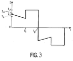
- the resulting current is shown in fig 3 .
- the current at the start of the period I1 is higher than Ie.
- the lamp current is provided with a pulse of the same polarity at the end of the period with a value 13.
- the value of 13 is 1,6Im.
Landscapes
- Circuit Arrangements For Discharge Lamps (AREA)
- Electrophonic Musical Instruments (AREA)
- Inductance-Capacitance Distribution Constants And Capacitance-Resistance Oscillators (AREA)
- Lock And Its Accessories (AREA)
- Selective Calling Equipment (AREA)
Abstract
Description
- The invention relates to a circuit arrangement for operating a high pressure discharge lamp having a rated power Pla and having during operation an electrode which is in a cathodic phase, comprising
- input terminals for connection to a supply voltage source,
- output terminals for connecting the high pressure discharge lamp, and
- means, coupled to the input terminals, for supplying an alternating lamp current having successive periods of opposite polarity to the high pressure discharge lamp, the lamp current per period having a mean value Im, corresponding to said rated power Pla.
- Such a circuit arrangement is known from
US 5608294 . In the known circuit the lamp current at each period is provided with a superposition of a current pulse in a latter part of each period. In case a high pressure discharge lamp is operated with an AC current, each electrode of the lamp alternatingly functions as a cathode and as an anode during successive periods of the lamp current. During these successive periods the electrode emitting the lamp current is said to be in the cathodic phase and the other electrode to be in the anodic phase respectively. Because the total amount of current through the lamp is increased at the end of each period of the lamp current by means of the current pulse, the temperature of the electrode is sufficiently raised to increase the stability of the discharge arc. Accordingly flickering of the high pressure discharge lamp can be substantially suppressed. Due to its flickering suppression properties the circuit arrangement is in particular suitable for operating a high pressure discharge lamp in a projection system like a projection television apparatus. - Lamps operated with the known circuit arrangement showed to have a continuos increase of the arc voltage over an operating time of several hundred hours, which voltage increase appeared to continue when the lamp was experimentally operated for several thousand hours. As a stable luminous output of the lamp being fairly constant over the life of the lamp is of vital importance for use in a projection system, a continuos arc voltage increase forms a serious draw back in reaching a long lamp live.
- The invention aims to provide a circuit arrangement for operating a high pressure discharge lamp in which the mentioned draw back is counter acted.
- According to the invention a circuit arrangement mentioned in the opening paragraph is for this purpose characterized in that the lamp current has a profile according to
claim 1. The arrangement has the advantage that during lamp operation the discharge arc has a soft start each period by diffusely attaching both electrodes resulting in a lower electrode load, so making it possible to operate the lamp without flickering over a long time together with a very significant reduction in occurrence of an increase of the arc voltage. - The mean value of the current Im over a period corresponds to the power Pla of the lamp according to the relation Pla=Im*Vla with Vla the lamp voltage. Experiments have learned that preferably the mean value of the current over a fist part of the period Ie is smaller than the value Im and over a second part of the period a mean current value I2 which is larger than Im. This further improves a soft current start at the beginning of each period with a diffuse arc attachment over the first part of the period resulting in a stabilized arc attachment. As a consequence of the current over the second part of the period I2 being larger than Im the need of an additional current pulse near the end of the period is further reduced.
- In a preferred embodiment of the arrangement according to the invention the period has a time duration tp and the first part of the period a time duration t1 which satisfies the relation .05≤t1/tp≤.85. In case of a value of the ratio t1/tp smaller than .05 experiments showed no measurable improvement over the prior art. The upper value of the ratio t1/tp depends on a compromise. For the diffuse stable attachment the ratio should be as long as possible. However as the cathode tends to cool during the cathode phase so the current which is emitted with a diffuse stable attachment tends to lower, this comes in conflict with the need of keeping the lamp operating at the requested power rate. So experimentally it was shown that for an increasing current shape in the first part of the period the ratio should preferably be at most .5. In the situation of a decreasing current during t1 the maximum ratio can be .85. Otherwise it has appeared that for the values of the currents Ie and Im a relation should be hold which reads .3≤Ie/Im≤.9 and preferable satisfies .6≤Ie/Im≤.8, resulting in a reduced extra load on the electrode in comparison to the prior art. For current values of Ie>.9Im no measurable effects have been found. If Ie becomes too low with respect to Im the value of the mean current in the second part of the period I2 must be chosen so high that there exists a serious risk on occurrence of arc instabilities during the second part of the period resulting in lamp flickering.
- According to the invention, the current at the start of the period is higher than Ie. In this way there is taken into account in an advantageous way that the cathode temperature lowers during the period and thus correspondingly the current value for which a stable diffuse attachment of the arc holds.
- Arc stabilization and therethrough reducing lamp flicker is still further promoted with adding to the lamp current an additional current pulse as known from the prior art. Preferably the lamp current is then provided with a pulse of the same polarity at the end of the period with a value 13 satisfying the relation I3≤2Im.
- The above and further aspects of the invention will be explained in more detail below with reference to a drawing, in which
-
Fig. 1 shows a schematic scheme of a circuit arrangement according to the invention, -
Fig. 2 shows control means of an embodiment of a circuit arrangement according to the invention in accordance withfig 1 , -
Fig 3 is a graph of a lamp current provided by the arrangement according tofig 1 . - In
fig 1 are means for generating a controlled dc supply current having input terminals K1,K2 for connecting to a supply voltage source supplying a supply voltage. Output terminals of means I are connected to respective input terminals of a commutator II. The commutator II is provided with output terminals L1,L2 for connecting a high pressure discharge lamp La. III are control means to control the value of the current supplied to the lamp by way of controlling the means I. The means I and the commutator II together constitute means, coupled to the input terminals, for supplying an alternating lamp current having successive periods of opposite polarity, the lamp current per period having a mean value Im. - The operation of the circuit arrangement shown in
fig 1 is as follows. - When input terminals K1,K2 are connected to a voltage supply source, means I generate a dc supply current from the supply voltage supplied by the voltage supply source. Commutator II converts this dc current into an alternating current having successive periods of opposite polarity. By control means III the value of the current thus formed and supplied to the lamp La is controlled such that the lamp current in each period at its start is lowered with respect to the mean value Im so as to allow for stable diffuse attack on the cathodic phase electrode. In a practical realization of the described embodiment the means I are formed by a rectifier bridge followed by a switch mode power circuit, for instance a Buck or down converter. Commutator II preferably comprises a full bridge circuit. Lamp ignition circuitry is preferably incorporated also in the commutator means II.
- In
Fig. 2 , the control means III for controlling means I are shown in more detail. The control means III comprise aninput 1 for detecting the arc voltage, for instance the voltage over the terminals L1,L2 connected to the lamp forming a signal representing the arc voltage and further called lamp voltage. Preferably the lamp voltage representing signal is formed by detecting a voltage at a connection point L3, as the thus detected voltage is a dc voltage which will not be disturbed by ignition voltages generated in the lamp ignition circuitry. Control means III further comprises, aninput 2 for detecting of the current through inductive means L of the converter forming the switch mode power circuit of the means I, which converter has at least a switch, and anoutput terminal 3 for switching the switch of the switch mode power circuit periodically in a conducting and a non-conducting state thus controlling the current through the induction means L of the converter.Input 1 is connected to connection pin P1 of a microcontroller MC. A connection pin P3 of the microcontroller is connected to an input 4 of a switching circuit SC.Input 2 is connected to aninput 5 of the switching circuit SC, of which an output O is connected tooutput terminal 3. - The operation of the circuit arrangement shown in
Fig. 2 with the converter being a Buck or down converter, is as follows. The microcontroller MC is provided with software containing a matrix of converter peak current values labeled to lamp voltage, time combinations, wherein the time is counted from the start of each period of the lamp current. A thus found converter peak current value is fed to switching circuit SC at input 4 and used as reference for comparison for the detected current atinput 2 which is also fed to the switching circuit SC, atinput 5. Based on this current values comparison the switching circuit generates a switching off signal at output O, which switches the switch of the down converter in the non- conducting state when the detected current equals the peak current value. As a result the current through the inductive means will decrease. The converter switch is kept in the non-conductive state until the current through the inductive means L becomes zero. On detecting the converter current becoming zero the switching circuit SC generates at its output O a switch on signal that renders the switch of the down converter conductive. The current through the inductive means L now starts to increase until it reaches the peak current value. Such switching circuit SC is for instance known fromWO97/14275 - The detection of the lamp voltage is done with a repetition rate during each period depending on the shape of the current to be realized through the lamp and is controlled by a built in timer of the microcontroller MC. Taking the lamp voltage as lamp parameter for detection has as an advantage that it makes possible to have a wattage control of the lamp inherently incorporated in the microcontroller software. In case the lamp current itself is taken as parameter for detection a wattage control would not only require an additional detection of the lamp voltage, but also an additional control procedure in the microcontroller. The down converter operates in a favourable embodiment at a frequency in the range of 45kHz to 75kHz.
- According to the invention the resulting current is shown in
fig 3 . In this case the current at the start of the period I1 is higher than Ie. - According to another preferred embodiment the lamp current is provided with a pulse of the same polarity at the end of the period with a value 13. In a practical realization of the described embodiment the value of 13 is 1,6Im.
Claims (4)
- Circuit arrangement for operating a high pressure discharge lamp having a rated power Pla and having during operation an electrode which is in a cathodic phase, comprising- input terminals for connection to a supply voltage source,- output terminals for connecting the high pressure discharge lamp, and- means, coupled to the input terminals, for supplying an alternating lamp current having successive periods of opposite polarity to the high pressure discharge lamp, the lamp current per period having a mean value Im, corresponding to the power Pla, characterized in that the lamp current in each period at its start is lowered with respect to the mean value Im and has over a first part of the period a lower mean value Ie so as to allow for stable diffuse attachment on the cathodic phase electrode, and in that the current at the start of the period is higher than Ie.
- Circuit arrangement according to claim 1, characterized in that the period has a time tp and the first part of the period a time duration tl which satisfies the relation 0.05 ≤ tl/tp ≤. 0.85.
- Circuit arrangement according to claim 1, or 2, characterized in that 0.3≤Ie/Im≤ 0.9.
- Circuit arrangement according to any of the preceding claims, characterized in that the lamp current is provided with a pulse of the same polarity at the end of the period with a value 13 satisfying the relation I3≤2Im.
Priority Applications (1)
| Application Number | Priority Date | Filing Date | Title |
|---|---|---|---|
| EP02080149A EP1296543B1 (en) | 1998-12-17 | 1999-12-02 | Circuit arrangement |
Applications Claiming Priority (4)
| Application Number | Priority Date | Filing Date | Title |
|---|---|---|---|
| EP98204287 | 1998-12-17 | ||
| EP98204287 | 1998-12-17 | ||
| EP02080149A EP1296543B1 (en) | 1998-12-17 | 1999-12-02 | Circuit arrangement |
| EP99964531A EP1057377B1 (en) | 1998-12-17 | 1999-12-02 | Circuit arrangement |
Related Parent Applications (2)
| Application Number | Title | Priority Date | Filing Date |
|---|---|---|---|
| EP99964531.0 Division | 1999-12-02 | ||
| EP99964531A Division EP1057377B1 (en) | 1998-12-17 | 1999-12-02 | Circuit arrangement |
Publications (3)
| Publication Number | Publication Date |
|---|---|
| EP1296543A2 EP1296543A2 (en) | 2003-03-26 |
| EP1296543A3 EP1296543A3 (en) | 2005-06-01 |
| EP1296543B1 true EP1296543B1 (en) | 2008-10-29 |
Family
ID=8234477
Family Applications (2)
| Application Number | Title | Priority Date | Filing Date |
|---|---|---|---|
| EP99964531A Expired - Lifetime EP1057377B1 (en) | 1998-12-17 | 1999-12-02 | Circuit arrangement |
| EP02080149A Expired - Lifetime EP1296543B1 (en) | 1998-12-17 | 1999-12-02 | Circuit arrangement |
Family Applications Before (1)
| Application Number | Title | Priority Date | Filing Date |
|---|---|---|---|
| EP99964531A Expired - Lifetime EP1057377B1 (en) | 1998-12-17 | 1999-12-02 | Circuit arrangement |
Country Status (9)
| Country | Link |
|---|---|
| US (1) | US6239556B1 (en) |
| EP (2) | EP1057377B1 (en) |
| JP (1) | JP4548940B2 (en) |
| KR (1) | KR100664335B1 (en) |
| CN (1) | CN1166258C (en) |
| AT (2) | ATE281752T1 (en) |
| DE (2) | DE69921616T2 (en) |
| TW (1) | TWM266672U (en) |
| WO (1) | WO2000036883A1 (en) |
Families Citing this family (22)
| Publication number | Priority date | Publication date | Assignee | Title |
|---|---|---|---|---|
| GB9825298D0 (en) * | 1998-11-18 | 1999-01-13 | Microlights Ltd | An electronic ballast |
| DE10018860A1 (en) * | 2000-04-14 | 2001-10-18 | Patent Treuhand Ges Fuer Elektrische Gluehlampen Mbh | Stabilization of the operation of gas discharge lamps |
| DE10021537A1 (en) * | 2000-05-03 | 2001-11-08 | Philips Corp Intellectual Pty | Method and device for operating a gas discharge lamp |
| JP4426132B2 (en) * | 2000-07-26 | 2010-03-03 | ハリソン東芝ライティング株式会社 | High pressure discharge lamp lighting method, high pressure discharge lamp lighting device, and illumination device |
| TW512376B (en) * | 2000-08-17 | 2002-12-01 | Koninkl Philips Electronics Nv | Switching device |
| JP2002134287A (en) | 2000-10-24 | 2002-05-10 | Tdk Corp | Electric discharge lamp lighting method and equipment |
| DE10062974A1 (en) * | 2000-12-16 | 2002-06-20 | Philips Corp Intellectual Pty | High pressure gas discharge lamp and process for its manufacture |
| US6476566B2 (en) | 2000-12-27 | 2002-11-05 | Infocus Systems, Inc. | Method and apparatus for canceling ripple current in a lamp |
| CN100562203C (en) * | 2003-02-19 | 2009-11-18 | 明基电通股份有限公司 | Projector with external power supply |
| JP4902528B2 (en) | 2004-05-05 | 2012-03-21 | アイマックス コーポレイション | Multi-light source high-performance stereoscopic projection system |
| JP4415377B2 (en) | 2004-06-24 | 2010-02-17 | セイコーエプソン株式会社 | Light source driving method and projector |
| US7323824B2 (en) * | 2004-08-03 | 2008-01-29 | Matsushita Electric Works Ltd. | Methods and apparatus for operating very high pressure short arc discharge lamps |
| US7250732B2 (en) * | 2004-09-30 | 2007-07-31 | General Electric Company | High pressure discharge lamp control system and method |
| US20100052561A1 (en) * | 2005-06-21 | 2010-03-04 | Koninklijke Philips Electronics, N.V. | Method for driving an inverter of a gas discharge supply circuit |
| US7443103B2 (en) * | 2005-06-24 | 2008-10-28 | General Electric Company | High pressure lamp with lamp flicker suppression and lamp voltage control |
| CN101351867B (en) | 2006-01-03 | 2011-11-16 | 皇家飞利浦电子股份有限公司 | High-pressure mercury vapor discharge lamp and method of manufacturing a high-pressure mercury vapor discharge lamp |
| GB2444977A (en) * | 2006-12-21 | 2008-06-25 | Gen Electric | An ultra high pressure mercury arc lamp |
| JP4470990B2 (en) * | 2007-10-31 | 2010-06-02 | セイコーエプソン株式会社 | Light source device, projector, and driving method of light source device |
| KR200449388Y1 (en) * | 2008-01-15 | 2010-07-07 | 진명홈바스(주) | Cleaning brush storage |
| JP4678414B2 (en) * | 2008-03-17 | 2011-04-27 | セイコーエプソン株式会社 | Discharge lamp lighting device, control method therefor, and projector |
| KR200454039Y1 (en) * | 2008-08-07 | 2011-06-14 | 정명식 | Ankle striking device |
| JP6155619B2 (en) | 2012-12-17 | 2017-07-05 | セイコーエプソン株式会社 | Projector and projection system |
Family Cites Families (4)
| Publication number | Priority date | Publication date | Assignee | Title |
|---|---|---|---|---|
| DE4410177A1 (en) * | 1994-03-24 | 1995-09-28 | Hella Kg Hueck & Co | Circuit for starting and running AC high-pressure gas discharge lamp |
| TW339496B (en) * | 1994-06-22 | 1998-09-01 | Philips Electronics Nv | Method and circuit arrangement for operating a high-pressure discharge lamp |
| DE4439885A1 (en) * | 1994-11-08 | 1996-05-09 | Bosch Gmbh Robert | Device for operating a gas discharge lamp |
| TW440123U (en) | 1995-10-09 | 2001-06-07 | Koninkl Philips Electronics Nv | A circuit arrangement for igniting and operating a high pressure discharge lamp |
-
1999
- 1999-12-01 TW TW093209797U patent/TWM266672U/en not_active IP Right Cessation
- 1999-12-02 DE DE69921616T patent/DE69921616T2/en not_active Expired - Lifetime
- 1999-12-02 EP EP99964531A patent/EP1057377B1/en not_active Expired - Lifetime
- 1999-12-02 AT AT99964531T patent/ATE281752T1/en not_active IP Right Cessation
- 1999-12-02 AT AT02080149T patent/ATE413088T1/en not_active IP Right Cessation
- 1999-12-02 EP EP02080149A patent/EP1296543B1/en not_active Expired - Lifetime
- 1999-12-02 DE DE69939845T patent/DE69939845D1/en not_active Expired - Lifetime
- 1999-12-02 WO PCT/EP1999/009594 patent/WO2000036883A1/en not_active Ceased
- 1999-12-02 KR KR1020007008931A patent/KR100664335B1/en not_active Expired - Fee Related
- 1999-12-02 CN CNB998028347A patent/CN1166258C/en not_active Expired - Lifetime
- 1999-12-02 JP JP2000589009A patent/JP4548940B2/en not_active Expired - Lifetime
- 1999-12-15 US US09/464,007 patent/US6239556B1/en not_active Expired - Lifetime
Also Published As
| Publication number | Publication date |
|---|---|
| KR20010072549A (en) | 2001-07-31 |
| DE69921616T2 (en) | 2005-09-15 |
| TWM266672U (en) | 2005-06-01 |
| EP1057377B1 (en) | 2004-11-03 |
| KR100664335B1 (en) | 2007-01-02 |
| ATE281752T1 (en) | 2004-11-15 |
| DE69921616D1 (en) | 2004-12-09 |
| CN1290470A (en) | 2001-04-04 |
| DE69939845D1 (en) | 2008-12-11 |
| WO2000036883A1 (en) | 2000-06-22 |
| CN1166258C (en) | 2004-09-08 |
| EP1296543A3 (en) | 2005-06-01 |
| US6239556B1 (en) | 2001-05-29 |
| EP1296543A2 (en) | 2003-03-26 |
| JP4548940B2 (en) | 2010-09-22 |
| EP1057377A1 (en) | 2000-12-06 |
| ATE413088T1 (en) | 2008-11-15 |
| JP2002532867A (en) | 2002-10-02 |
Similar Documents
| Publication | Publication Date | Title |
|---|---|---|
| EP1057377B1 (en) | Circuit arrangement | |
| EP1057376B1 (en) | Circuit arrangement | |
| EP0658921B1 (en) | Low-pressure mercury discharge lamp | |
| US5608294A (en) | High pressure lamp operating circuit with suppression of lamp flicker | |
| EP0797906B1 (en) | Circuit arrangement | |
| EP0595414A2 (en) | Electronic ballast for a high intensity discharge lamp | |
| US8593077B2 (en) | High-voltage discharge lamp lighting device and lighting fixture | |
| EP1964453A1 (en) | Dimming ballast and method | |
| CN1291418A (en) | Circuit arrangement | |
| JP2003059684A (en) | High pressure discharge lamp device | |
| EP0797905B1 (en) | Circuit arrangement | |
| US20070145905A1 (en) | Driver device for a gas discharge lamp and igniter | |
| US6385068B2 (en) | Circuit device | |
| US7154228B2 (en) | Ballast for high pressure discharge lamp | |
| EP1314338B1 (en) | Circuit device | |
| KR20000026289A (en) | Automatic turning on/off system for fluorescent lamp | |
| KR100505756B1 (en) | Instantaneous electornic ballast stabilizer of Metal Halide Discharge Lamp having takeover current circuit |
Legal Events
| Date | Code | Title | Description |
|---|---|---|---|
| PUAI | Public reference made under article 153(3) epc to a published international application that has entered the european phase |
Free format text: ORIGINAL CODE: 0009012 |
|
| AC | Divisional application: reference to earlier application |
Ref document number: 1057377 Country of ref document: EP Kind code of ref document: P |
|
| AK | Designated contracting states |
Kind code of ref document: A2 Designated state(s): AT BE DE FR GB NL |
|
| PUAL | Search report despatched |
Free format text: ORIGINAL CODE: 0009013 |
|
| AK | Designated contracting states |
Kind code of ref document: A3 Designated state(s): AT BE DE FR GB NL |
|
| 17P | Request for examination filed |
Effective date: 20051201 |
|
| AKX | Designation fees paid |
Designated state(s): AT BE DE FR GB NL |
|
| 17Q | First examination report despatched |
Effective date: 20070118 |
|
| GRAP | Despatch of communication of intention to grant a patent |
Free format text: ORIGINAL CODE: EPIDOSNIGR1 |
|
| GRAS | Grant fee paid |
Free format text: ORIGINAL CODE: EPIDOSNIGR3 |
|
| GRAA | (expected) grant |
Free format text: ORIGINAL CODE: 0009210 |
|
| AC | Divisional application: reference to earlier application |
Ref document number: 1057377 Country of ref document: EP Kind code of ref document: P |
|
| AK | Designated contracting states |
Kind code of ref document: B1 Designated state(s): AT BE DE FR GB NL |
|
| REG | Reference to a national code |
Ref country code: GB Ref legal event code: FG4D |
|
| REF | Corresponds to: |
Ref document number: 69939845 Country of ref document: DE Date of ref document: 20081211 Kind code of ref document: P |
|
| NLV1 | Nl: lapsed or annulled due to failure to fulfill the requirements of art. 29p and 29m of the patents act | ||
| PG25 | Lapsed in a contracting state [announced via postgrant information from national office to epo] |
Ref country code: AT Free format text: LAPSE BECAUSE OF FAILURE TO SUBMIT A TRANSLATION OF THE DESCRIPTION OR TO PAY THE FEE WITHIN THE PRESCRIBED TIME-LIMIT Effective date: 20081029 |
|
| PG25 | Lapsed in a contracting state [announced via postgrant information from national office to epo] |
Ref country code: NL Free format text: LAPSE BECAUSE OF FAILURE TO SUBMIT A TRANSLATION OF THE DESCRIPTION OR TO PAY THE FEE WITHIN THE PRESCRIBED TIME-LIMIT Effective date: 20081029 |
|
| PG25 | Lapsed in a contracting state [announced via postgrant information from national office to epo] |
Ref country code: BE Free format text: LAPSE BECAUSE OF FAILURE TO SUBMIT A TRANSLATION OF THE DESCRIPTION OR TO PAY THE FEE WITHIN THE PRESCRIBED TIME-LIMIT Effective date: 20081029 |
|
| PLBE | No opposition filed within time limit |
Free format text: ORIGINAL CODE: 0009261 |
|
| STAA | Information on the status of an ep patent application or granted ep patent |
Free format text: STATUS: NO OPPOSITION FILED WITHIN TIME LIMIT |
|
| 26N | No opposition filed |
Effective date: 20090730 |
|
| REG | Reference to a national code |
Ref country code: DE Ref legal event code: R082 Ref document number: 69939845 Country of ref document: DE Representative=s name: MEISSNER, BOLTE & PARTNER GBR, DE |
|
| REG | Reference to a national code |
Ref country code: DE Ref legal event code: R082 Ref document number: 69939845 Country of ref document: DE Representative=s name: MEISSNER BOLTE PATENTANWAELTE RECHTSANWAELTE P, DE Effective date: 20140328 Ref country code: DE Ref legal event code: R081 Ref document number: 69939845 Country of ref document: DE Owner name: KONINKLIJKE PHILIPS N.V., NL Free format text: FORMER OWNER: KONINKLIJKE PHILIPS ELECTRONICS N.V., EINDHOVEN, NL Effective date: 20140328 Ref country code: DE Ref legal event code: R082 Ref document number: 69939845 Country of ref document: DE Representative=s name: MEISSNER, BOLTE & PARTNER GBR, DE Effective date: 20140328 Ref country code: DE Ref legal event code: R081 Ref document number: 69939845 Country of ref document: DE Owner name: PHILIPS LIGHTING HOLDING B.V., NL Free format text: FORMER OWNER: KONINKLIJKE PHILIPS ELECTRONICS N.V., EINDHOVEN, NL Effective date: 20140328 |
|
| REG | Reference to a national code |
Ref country code: FR Ref legal event code: CD Owner name: KONINKLIJKE PHILIPS N.V., NL Effective date: 20141126 Ref country code: FR Ref legal event code: CA Effective date: 20141126 |
|
| REG | Reference to a national code |
Ref country code: FR Ref legal event code: PLFP Year of fee payment: 17 |
|
| REG | Reference to a national code |
Ref country code: GB Ref legal event code: 732E Free format text: REGISTERED BETWEEN 20161006 AND 20161012 |
|
| REG | Reference to a national code |
Ref country code: FR Ref legal event code: PLFP Year of fee payment: 18 |
|
| PGFP | Annual fee paid to national office [announced via postgrant information from national office to epo] |
Ref country code: GB Payment date: 20161228 Year of fee payment: 18 |
|
| REG | Reference to a national code |
Ref country code: DE Ref legal event code: R082 Ref document number: 69939845 Country of ref document: DE Representative=s name: MEISSNER BOLTE PATENTANWAELTE RECHTSANWAELTE P, DE Ref country code: DE Ref legal event code: R081 Ref document number: 69939845 Country of ref document: DE Owner name: PHILIPS LIGHTING HOLDING B.V., NL Free format text: FORMER OWNER: KONINKLIJKE PHILIPS N.V., EINDHOVEN, NL |
|
| PGFP | Annual fee paid to national office [announced via postgrant information from national office to epo] |
Ref country code: DE Payment date: 20170228 Year of fee payment: 18 |
|
| REG | Reference to a national code |
Ref country code: FR Ref legal event code: PLFP Year of fee payment: 19 |
|
| REG | Reference to a national code |
Ref country code: DE Ref legal event code: R119 Ref document number: 69939845 Country of ref document: DE |
|
| GBPC | Gb: european patent ceased through non-payment of renewal fee |
Effective date: 20171202 |
|
| PG25 | Lapsed in a contracting state [announced via postgrant information from national office to epo] |
Ref country code: DE Free format text: LAPSE BECAUSE OF NON-PAYMENT OF DUE FEES Effective date: 20180703 |
|
| PG25 | Lapsed in a contracting state [announced via postgrant information from national office to epo] |
Ref country code: GB Free format text: LAPSE BECAUSE OF NON-PAYMENT OF DUE FEES Effective date: 20171202 |
|
| PGFP | Annual fee paid to national office [announced via postgrant information from national office to epo] |
Ref country code: FR Payment date: 20181231 Year of fee payment: 20 |