EP1296166A1 - Optical demultiplexing device with optical to electrical conversion - Google Patents
Optical demultiplexing device with optical to electrical conversion Download PDFInfo
- Publication number
- EP1296166A1 EP1296166A1 EP02013260A EP02013260A EP1296166A1 EP 1296166 A1 EP1296166 A1 EP 1296166A1 EP 02013260 A EP02013260 A EP 02013260A EP 02013260 A EP02013260 A EP 02013260A EP 1296166 A1 EP1296166 A1 EP 1296166A1
- Authority
- EP
- European Patent Office
- Prior art keywords
- optical
- demultiplexer
- signal
- recited
- photodetectors
- Prior art date
- Legal status (The legal status is an assumption and is not a legal conclusion. Google has not performed a legal analysis and makes no representation as to the accuracy of the status listed.)
- Withdrawn
Links
- 230000003287 optical effect Effects 0.000 title claims abstract description 65
- 238000006243 chemical reaction Methods 0.000 title claims description 4
- 238000000034 method Methods 0.000 claims description 9
- 239000000835 fiber Substances 0.000 description 23
- 238000003491 array Methods 0.000 description 4
- 230000005540 biological transmission Effects 0.000 description 3
- 239000013078 crystal Substances 0.000 description 2
- 238000010586 diagram Methods 0.000 description 2
- 239000006185 dispersion Substances 0.000 description 2
- 238000003780 insertion Methods 0.000 description 2
- 230000037431 insertion Effects 0.000 description 2
- 238000004519 manufacturing process Methods 0.000 description 2
- 239000013307 optical fiber Substances 0.000 description 2
- 238000005253 cladding Methods 0.000 description 1
- 238000004891 communication Methods 0.000 description 1
- 230000008602 contraction Effects 0.000 description 1
- 238000001514 detection method Methods 0.000 description 1
- 230000007613 environmental effect Effects 0.000 description 1
- 238000011084 recovery Methods 0.000 description 1
Images


Classifications
-
- G—PHYSICS
- G02—OPTICS
- G02B—OPTICAL ELEMENTS, SYSTEMS OR APPARATUS
- G02B6/00—Light guides; Structural details of arrangements comprising light guides and other optical elements, e.g. couplings
- G02B6/24—Coupling light guides
- G02B6/42—Coupling light guides with opto-electronic elements
- G02B6/4201—Packages, e.g. shape, construction, internal or external details
- G02B6/4204—Packages, e.g. shape, construction, internal or external details the coupling comprising intermediate optical elements, e.g. lenses, holograms
- G02B6/4215—Packages, e.g. shape, construction, internal or external details the coupling comprising intermediate optical elements, e.g. lenses, holograms the intermediate optical elements being wavelength selective optical elements, e.g. variable wavelength optical modules or wavelength lockers
-
- G—PHYSICS
- G02—OPTICS
- G02B—OPTICAL ELEMENTS, SYSTEMS OR APPARATUS
- G02B6/00—Light guides; Structural details of arrangements comprising light guides and other optical elements, e.g. couplings
- G02B6/24—Coupling light guides
- G02B6/26—Optical coupling means
- G02B6/28—Optical coupling means having data bus means, i.e. plural waveguides interconnected and providing an inherently bidirectional system by mixing and splitting signals
- G02B6/293—Optical coupling means having data bus means, i.e. plural waveguides interconnected and providing an inherently bidirectional system by mixing and splitting signals with wavelength selective means
- G02B6/29304—Optical coupling means having data bus means, i.e. plural waveguides interconnected and providing an inherently bidirectional system by mixing and splitting signals with wavelength selective means operating by diffraction, e.g. grating
- G02B6/29305—Optical coupling means having data bus means, i.e. plural waveguides interconnected and providing an inherently bidirectional system by mixing and splitting signals with wavelength selective means operating by diffraction, e.g. grating as bulk element, i.e. free space arrangement external to a light guide
- G02B6/2931—Diffractive element operating in reflection
-
- G—PHYSICS
- G02—OPTICS
- G02B—OPTICAL ELEMENTS, SYSTEMS OR APPARATUS
- G02B6/00—Light guides; Structural details of arrangements comprising light guides and other optical elements, e.g. couplings
- G02B6/24—Coupling light guides
- G02B6/26—Optical coupling means
- G02B6/28—Optical coupling means having data bus means, i.e. plural waveguides interconnected and providing an inherently bidirectional system by mixing and splitting signals
- G02B6/293—Optical coupling means having data bus means, i.e. plural waveguides interconnected and providing an inherently bidirectional system by mixing and splitting signals with wavelength selective means
- G02B6/29379—Optical coupling means having data bus means, i.e. plural waveguides interconnected and providing an inherently bidirectional system by mixing and splitting signals with wavelength selective means characterised by the function or use of the complete device
- G02B6/2938—Optical coupling means having data bus means, i.e. plural waveguides interconnected and providing an inherently bidirectional system by mixing and splitting signals with wavelength selective means characterised by the function or use of the complete device for multiplexing or demultiplexing, i.e. combining or separating wavelengths, e.g. 1xN, NxM
Definitions
- the present invention relates to optical communication devices. More specifically, the present invention relates to an optical demultiplexer and optical to electrical signal conversion.
- Figure 1 illustrates a simplified block diagram of such a hybrid network including first and second electronic devices 10 and 12, electric signal to optical signal device (EOD) 14, optical signal to electric signal device (OED) 16, an optical multiplexer (MUX) 18, and an optical demultiplexer (DEMUX) 20.
- EOD electric signal to optical signal device
- OED optical signal to electric signal device
- MUX optical multiplexer
- DEMUX optical demultiplexer
- E1, E2, ..., EN Electrical signals, or channels, designated herein as E1, E2, ..., EN, are provided by the first electronic device 10 to the EOD 14.
- signals and “channel” are used interchangeably.
- the EOD 14 converts the electronic signals to optical signals, or channels, L1, L2, ..., LN where the electrical channel E1 corresponds to the optical channel L1, E2 corresponds to L2, and so forth, and where each optical channel has a different carrier wavelength.
- the optical channels L1, L2, ..., LN are multiplexed by the MUX 18 into a single wave division multiplexed (WDM) signal 11, which is then transmitted.
- WDM wave division multiplexed
- the WDM signal 11 is demultiplexed by the DEMUX 20 into its component channels, L1a, L2a, ..., LNa where the demultiplexed channel L1a corresponds to the channel L1, L2a corresponds to L1, and so forth.
- Each of the demultiplexed optical channels is converted back into its corresponding electrical channels by the OED 16 for further processing by a second electrical device 12.
- directional arrows, or rays, such as ray 11 and others are used to indicate general direction of transmission of various optical or electrical signals and are not used to represent ray traces as often used in the optic arts.
- the optical DEMUX 20 takes a WDM signal 11 (carried on a single-mode optical fiber 22) as its input.
- the WDM signal 11 is demultiplexed by a complex configuration of optical elements 30 for dispersion of the WDM signal 11 into its component channels, L1, L2, ..., LN.
- the optical elements 30 can include intricate arrangements of various combinations of optical devices such as lenses, mirrors, crystals, rotators, wave-guides, reflectors, gratings, polarizers, beam splitters, filters, and collimators.
- the optical elements 30 are represented only by lenses 24 and 26 and diffractive grating surface 28; however, in actual implementations of the DEMUX 20, the optical elements 30 are numerous and in complex configuration, and many different implementations are possible.
- the demultiplexed, or separated, optical channels L1a, L2a, ..., LNa are focused on an output image plane 32 for insertion into output fibers F1, F2, ..., FN.
- the output plane 32 is a plane where receiving ends of output fibers are positioned such that each of the separated optical channels is focused for insertion into its corresponding output fiber.
- the channel L1a is focused on the output plane 32 aligned with the end of the output fiber F1
- the channel L2a is focused and aligned with the end of the output fiber F2, and so forth.
- the demultiplexed optical channels are delivered from the DEMUX 20 to the OED 16 via the output fibers F1, F2, ..., FN.
- the output fibers are illustrated, for clarity, as separately positioned from each other; however, in practice, they may be bunched together as a fiber bundle or ribbon.
- the OED 16 converts each of the optical signals into electrical signals E1a, E2a, ..., ENa.
- the OED 16 can include a plurality of optic to electrical converters 16a, 16b, ..., 16n.
- each of the output fibers F1, F2, ..., FN are single-mode fibers having very small circular core diameter and having small capture angle.
- the capture angle can be regarded as the maximum incidence angle at which an optical signal presented to the input of the optical fiber will be launched into the core of the fiber.
- Figure 2B illustrates a cross-section of the output fibers at the output image plane 32 viewed from line A-A of figure 2A.
- Each of these fibers may have a diameter of about 250 microns; however, most of that is cladding, and the circular core (for example core 34) diameter is only about 10 microns or less. Further, each of these fibers may have a capture angle of 6 degrees or smaller. Consequently, when the WDM signal 11 is demultiplexed and directed toward the output fibers, each of the demultiplexed channels must be aligned with its corresponding fiber core within a very small tolerance.
- the demultiplexed channel L1a must be aligned to the 10-micron core 34 of fiber F1 with a positional tolerance of the order of a micron, and an angular tolerance of the order of 1 degree.
- Some magnification systems relax the positional tolerance, but only at the expense of tighter angular tolerance.
- this alignment must e maintained over a wide temperature range, in the presence of extreme mechanical vibrations, over twenty years.
- the demultiplexer 20 is costly to manufacture.
- Each of the optical elements 30, the input fiber 22, and the output fibers F1, F2, ..., FN must be positioned with precision. Further, these must be affixed to a package such that the operation or movement of the device 20 does not cause misalignment of the demultiplexed optical channels to the output fibers.
- the demultiplexer 20 is susceptible to environmental effects such as temperature. For example, temperature-related expansion or contraction of any of the intricate parts of the demultiplexer 20 causes misalignment of the demultiplexed optical channels to the output fibers.
- dispersive means separates an optical wave division multiplexed (WDM) signal into its component optical signals. Then, a photodetector array converts the component optical signals into electrical signals.
- WDM optical wave division multiplexed
- a method of demultiplexing an optical wave division multiplexed (WDM) signal is disclosed. First, the WDM signal is separated into its component optical signals. Then, the component optical signals are detected by photodetectors for conversion to electrical signals.
- WDM optical wave division multiplexed
- Figure 1 illustrates a simplified block diagram of a wavelength-division multiplexed optical transmission system
- Figure 2A illustrates an implementation of the demultiplexer in Figure 1, using a diffraction grating
- Figure 2B illustrates the demultiplexer of Figure 2A along line A-A;
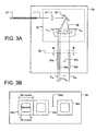
- Figure 3A illustrates an optical demultiplexer according to one embodiment of the present invention.
- Figure 3B illustrates the demultiplexer of Figure 3A along line B-B.
- the present invention is embodied in an optical apparatus including dispersive means for separating an optical wave division multiplexed (WDM) signal into its component optical signals and a photodetector array for converting the component optical signals into electrical signals.
- the photodetector array can be fabricated with detectors about 150 microns in width. This is more than 15 times the core diameter of a single-mode output fiber used in the prior art demultiplexers. Further, the detection efficiency of the photodetectors is largely independent of incidence angle. This is in contrast to the single-mode fibers of the prior art demultiplexers, in which launch efficiency falls off dramatically for incidence angles that deviate from 90 degrees by more than about 6 degrees. Accordingly, the manufacturing process is less costly, and a demultiplexer according to the present invention is less sensitive to temperature variations and vibrations.
- FIG 3A illustrates an optical demultiplexer (DEMUX) 50 according to one embodiment of the present invention.
- the DEMUX 50 of Figure 3A is illustrated using certain portions that are similar to those shown in Figure 2A.
- portions of the DEMUX 50 that are similar to portions of the DEMUX 20 of Figure 2A are assigned the same reference numerals and different portions are assigned different reference numerals.
- a WDM signal 11 enters the DEMUX 50 and is dispersed into its component optical channels L1a, L2a, ..., LNa.
- a group of optical elements 30 may be used for the dispersion of the WDM signal 11 into its component channels.
- the optical elements 30 are represented only by lenses 24 and 26 and surface diffraction grating 28; however, in actual implementations of the DEMUX 50, the optical elements 30 can be numerous and in complex configuration, including (but not limited to) microlens arrays, walkoff crystals, waveplates, colimating lenses, focussing lenses, mirrors, and prisms.
- the dispersed optical channels, or signals are directed toward an output image plane 52 where they are detected by an array of photodetectors.
- Each optical channel is incident on a separate photodetector.
- the array of photodetectors are represented by photodetectors 54a, 54b, and 54c along with an ellipsis 54d and collectively referred to using reference number 54.
- Each photodetector of the photodetector array 54 is aligned at the output plane 52 to detect one of the component optical channels and convert the detected signal into a corresponding electrical signal.
- Figure 3B illustrates cross section of the photodetector array 54 as seen at the output image plane 52 viewed from line B-B of figure 3A.
- the photodetectors can be separated by about 250 microns, for example, and have a sensor portion that can be about 150 microns wide.
- each photodetector of the photodetector array 54 can include integrated electronic amplifier to amplify the converted signal or include other electronic processing circuits, for example tansimpedance amplifiers, limiting amplifiers, and clock and data recovery circuits.
- the photodetector may be referred to as a photoreceiver.
- output electronic signals E1a, E2a, ..., ENa of the DEMUX 50 can be coupled directly into electronic post-amplifiers or processing on a separate integrated circuit (not shown).
- the photodetectors of the array 54 may be flip-chip bonded to bonded to other electronic components.
- the photodetector array 54 can be configured as a one-dimensional or a two-dimensional array. In fact, the photodetector array 54 can be built using sets of smaller arrays. For example, a linear photodetector array of 40 detectors may be made up of four monolithic arrays of ten detectors each.
- Photodetectors and photodetector arrays are available in the marketplace. For example only, see various optics components including optical signal monitors and detectors available from Sensors Unlimited, Inc. of Princeton, New Jersey and other vendors of optics components.
Landscapes
- Physics & Mathematics (AREA)
- General Physics & Mathematics (AREA)
- Optics & Photonics (AREA)
- Optical Communication System (AREA)
Abstract
Description
Claims (12)
- An optical demultiplexer (50) comprising:dispersive means (30) for separating an optical wave division multiplexed (WDM) signal (11) to its component optical signals;a photodetector array (54) for converting the component optical signals into electrical signals.
- The demultiplexer (50) recited in claim 1 wherein the photodetector array (54) is aligned at an output plane (52) to detect the component optical signals.
- The demultiplexer (50) recited in claim 1 wherein each photodetector of the photodetector array (54) includes integrated electronic amplifier.
- The demultiplexer (50) recited in claim 1 wherein the dispersive means (30) includes a surface diffraction grating (28).
- The demultiplexer (50) recited in claim 1 wherein the photodetector array (54) is a two-dimensional array.
- The demultiplexer (50) recited in claim 1 wherein the photodetectors of the photodetector array (54) are flip-chip bonded to other electronic components.
- A method of demultiplexing an optical wave division multiplexed (WDM) signal (11), the method comprising:dispersing the WDM signal (11) into its component optical signals; anddetecting the component optical signals with photodetectors (54) for conversion to electrical signals.
- The method recited in claim 7 wherein each photodetector includes integrated electronic amplifier.
- The method recited in claim 7 wherein the photodetectors (54) are aligned at an output plane (52) to detect the component optical signals.
- The method recited in claim 7 wherein a surface diffraction grating (28) is used for dispersing the WDM signal (11).
- The method recited in claim 7 wherein the photodetectors (54) are configured into a two dimensional array.
- The method recited in claim 7 wherein the photodetectors (54) are flip-chip bonded to other electronic components.
Applications Claiming Priority (2)
| Application Number | Priority Date | Filing Date | Title |
|---|---|---|---|
| US962635 | 2001-09-25 | ||
| US09/962,635 US20030058498A1 (en) | 2001-09-25 | 2001-09-25 | Optical demultiplexing device with optical to electrical conversion |
Publications (1)
| Publication Number | Publication Date |
|---|---|
| EP1296166A1 true EP1296166A1 (en) | 2003-03-26 |
Family
ID=25506167
Family Applications (1)
| Application Number | Title | Priority Date | Filing Date |
|---|---|---|---|
| EP02013260A Withdrawn EP1296166A1 (en) | 2001-09-25 | 2002-06-17 | Optical demultiplexing device with optical to electrical conversion |
Country Status (3)
| Country | Link |
|---|---|
| US (1) | US20030058498A1 (en) |
| EP (1) | EP1296166A1 (en) |
| JP (1) | JP2003139987A (en) |
Families Citing this family (1)
| Publication number | Priority date | Publication date | Assignee | Title |
|---|---|---|---|---|
| JP2007273315A (en) * | 2006-03-31 | 2007-10-18 | Sanyo Electric Co Ltd | Pack battery |
Citations (9)
| Publication number | Priority date | Publication date | Assignee | Title |
|---|---|---|---|---|
| US4696536A (en) * | 1985-07-01 | 1987-09-29 | The United States Of America As Represented By The Secretary Of The Navy | Integrated optical wavelength demultiplexer |
| JPS63115111A (en) * | 1986-10-31 | 1988-05-19 | Matsushita Electric Ind Co Ltd | Light wavelength demultiplexing detector |
| WO1992011517A1 (en) * | 1990-12-21 | 1992-07-09 | The Boeing Company | Planar waveguide spectrograph |
| FR2680012A1 (en) * | 1991-07-30 | 1993-02-05 | Sextant Avionique | Spectral dispersion device |
| EP0654917A2 (en) * | 1993-11-12 | 1995-05-24 | AT&T Corp. | High-density optical wavelength division multiplexing |
| EP1008878A1 (en) * | 1998-12-09 | 2000-06-14 | Nippon Sheet Glass Co., Ltd. | Optical wavelength demultiplexer |
| EP1219995A2 (en) * | 2000-12-26 | 2002-07-03 | Nippon Sheet Glass Co., Ltd. | Light-sensitive detector and optical demultiplexer |
| EP1271207A2 (en) * | 2001-03-13 | 2003-01-02 | Nippon Sheet Glass Co., Ltd. | Optical module and method of producing the same |
| EP1357412A1 (en) * | 2000-12-27 | 2003-10-29 | Nippon Sheet Glass Co., Ltd. | Method for aligning and assembling optical demultiplexer module, and automatic aligning mechanism |
Family Cites Families (6)
| Publication number | Priority date | Publication date | Assignee | Title |
|---|---|---|---|---|
| US4912545A (en) * | 1987-09-16 | 1990-03-27 | Irvine Sensors Corporation | Bonding of aligned conductive bumps on adjacent surfaces |
| US4839884A (en) * | 1988-03-04 | 1989-06-13 | General Electric Company | Multiple wavelength optical source and multiplexed light communication system |
| US6421179B1 (en) * | 1997-05-02 | 2002-07-16 | Interscience, Inc. | Wavelength division multiplexing system and method using a reconfigurable diffraction grating |
| EP0982616A4 (en) * | 1998-03-11 | 2003-03-19 | Nippon Sheet Glass Co Ltd | OPTICAL DEMULTIPLEXER |
| US6307657B1 (en) * | 1998-07-17 | 2001-10-23 | Lucent Technologies Inc. | Optomechanical platform |
| US6920290B2 (en) * | 2001-07-11 | 2005-07-19 | Lockheed Martin Corporation | Multi-wavelength high bandwidth communication receiver and system |
-
2001
- 2001-09-25 US US09/962,635 patent/US20030058498A1/en not_active Abandoned
-
2002
- 2002-06-17 EP EP02013260A patent/EP1296166A1/en not_active Withdrawn
- 2002-09-25 JP JP2002278697A patent/JP2003139987A/en not_active Withdrawn
Patent Citations (9)
| Publication number | Priority date | Publication date | Assignee | Title |
|---|---|---|---|---|
| US4696536A (en) * | 1985-07-01 | 1987-09-29 | The United States Of America As Represented By The Secretary Of The Navy | Integrated optical wavelength demultiplexer |
| JPS63115111A (en) * | 1986-10-31 | 1988-05-19 | Matsushita Electric Ind Co Ltd | Light wavelength demultiplexing detector |
| WO1992011517A1 (en) * | 1990-12-21 | 1992-07-09 | The Boeing Company | Planar waveguide spectrograph |
| FR2680012A1 (en) * | 1991-07-30 | 1993-02-05 | Sextant Avionique | Spectral dispersion device |
| EP0654917A2 (en) * | 1993-11-12 | 1995-05-24 | AT&T Corp. | High-density optical wavelength division multiplexing |
| EP1008878A1 (en) * | 1998-12-09 | 2000-06-14 | Nippon Sheet Glass Co., Ltd. | Optical wavelength demultiplexer |
| EP1219995A2 (en) * | 2000-12-26 | 2002-07-03 | Nippon Sheet Glass Co., Ltd. | Light-sensitive detector and optical demultiplexer |
| EP1357412A1 (en) * | 2000-12-27 | 2003-10-29 | Nippon Sheet Glass Co., Ltd. | Method for aligning and assembling optical demultiplexer module, and automatic aligning mechanism |
| EP1271207A2 (en) * | 2001-03-13 | 2003-01-02 | Nippon Sheet Glass Co., Ltd. | Optical module and method of producing the same |
Non-Patent Citations (1)
| Title |
|---|
| PATENT ABSTRACTS OF JAPAN vol. 012, no. 363 (P - 764) 29 September 1988 (1988-09-29) * |
Also Published As
| Publication number | Publication date |
|---|---|
| US20030058498A1 (en) | 2003-03-27 |
| JP2003139987A (en) | 2003-05-14 |
Similar Documents
| Publication | Publication Date | Title |
|---|---|---|
| USRE47906E1 (en) | Reconfigurable optical add-drop multiplexers with servo control and dynamic spectral power management capabilities | |
| US6307657B1 (en) | Optomechanical platform | |
| US5905824A (en) | Temperature compensated insensitive optical multiplexor/demultiplexor | |
| CN213659025U (en) | Light receiving assembly and optical module | |
| US6529652B1 (en) | Optical switch and method for aligning optical switch components | |
| WO2001007951A1 (en) | Compact double-pass wavelength multiplexer-demultiplexer having an increased number of channels | |
| US6134359A (en) | Optical multiplexing/demultiplexing device having a wavelength dispersive element | |
| WO2002067475A2 (en) | Wavelength division multiplexed device | |
| KR20140079540A (en) | Optical receiver module using wavelength division multiplexing type | |
| US10756839B1 (en) | Hybrid coarse wavelength division multiplexing (CWDM) transceiver | |
| JP2005309370A (en) | Optical module, optical multiplexer / demultiplexer, and optical multiplexer / demultiplexer unit using the same | |
| US6842239B2 (en) | Alignment of multi-channel diffractive WDM device | |
| US6256436B1 (en) | Optical wavelength demultiplexer | |
| US20030058498A1 (en) | Optical demultiplexing device with optical to electrical conversion | |
| Chan et al. | 1092 channel 2-D array demultiplexer for ultralarge data bandwidth | |
| JP2004361660A (en) | Array waveguide type wavelength demultiplexer | |
| US7277607B2 (en) | Optical multiplexer/demultiplexer, optical device, and optical transmission system | |
| JP2003066271A (en) | Optical wavelength demultiplexer | |
| US7139447B1 (en) | Angular dispersion amplification method and apparatus for optical demultiplexing | |
| JP5128444B2 (en) | Wavelength monitoring device | |
| KR100539313B1 (en) | Add/Drop Multiplexer having multiple input/output ports and plural filters | |
| US20020131705A1 (en) | Arrayed waveguide grating | |
| JP2004191460A (en) | Optical transceiver module | |
| GB2191646A (en) | Fibre optic transversal filter | |
| CA2246570C (en) | Optical demultiplexing/multiplexing device having a wavelength dependent element |
Legal Events
| Date | Code | Title | Description |
|---|---|---|---|
| PUAI | Public reference made under article 153(3) epc to a published international application that has entered the european phase |
Free format text: ORIGINAL CODE: 0009012 |
|
| AK | Designated contracting states |
Kind code of ref document: A1 Designated state(s): AT BE CH CY DE DK ES FI FR GB GR IE IT LI LU MC NL PT SE TR Designated state(s): AT BE CH CY DE DK ES FI FR GB GR IE IT LI LU MC NL PT SE TR |
|
| AX | Request for extension of the european patent |
Extension state: AL LT LV MK RO SI |
|
| 17P | Request for examination filed |
Effective date: 20030508 |
|
| AKX | Designation fees paid |
Designated state(s): DE FR GB IT |
|
| 17Q | First examination report despatched |
Effective date: 20031209 |
|
| STAA | Information on the status of an ep patent application or granted ep patent |
Free format text: STATUS: THE APPLICATION HAS BEEN WITHDRAWN |
|
| 18W | Application withdrawn |
Effective date: 20040119 |