EP1296162A1 - Polygon reflector, and illumination optical system and semiconductor exposure device using the polygon reflector - Google Patents
Polygon reflector, and illumination optical system and semiconductor exposure device using the polygon reflector Download PDFInfo
- Publication number
- EP1296162A1 EP1296162A1 EP02700713A EP02700713A EP1296162A1 EP 1296162 A1 EP1296162 A1 EP 1296162A1 EP 02700713 A EP02700713 A EP 02700713A EP 02700713 A EP02700713 A EP 02700713A EP 1296162 A1 EP1296162 A1 EP 1296162A1
- Authority
- EP
- European Patent Office
- Prior art keywords
- reflecting mirror
- multifaceted
- mirror elements
- elements
- placement plate
- Prior art date
- Legal status (The legal status is an assumption and is not a legal conclusion. Google has not performed a legal analysis and makes no representation as to the accuracy of the status listed.)
- Withdrawn
Links
Images








Classifications
-
- G—PHYSICS
- G03—PHOTOGRAPHY; CINEMATOGRAPHY; ANALOGOUS TECHNIQUES USING WAVES OTHER THAN OPTICAL WAVES; ELECTROGRAPHY; HOLOGRAPHY
- G03F—PHOTOMECHANICAL PRODUCTION OF TEXTURED OR PATTERNED SURFACES, e.g. FOR PRINTING, FOR PROCESSING OF SEMICONDUCTOR DEVICES; MATERIALS THEREFOR; ORIGINALS THEREFOR; APPARATUS SPECIALLY ADAPTED THEREFOR
- G03F7/00—Photomechanical, e.g. photolithographic, production of textured or patterned surfaces, e.g. printing surfaces; Materials therefor, e.g. comprising photoresists; Apparatus specially adapted therefor
- G03F7/70—Microphotolithographic exposure; Apparatus therefor
- G03F7/70058—Mask illumination systems
- G03F7/70141—Illumination system adjustment, e.g. adjustments during exposure or alignment during assembly of illumination system
-
- G—PHYSICS
- G02—OPTICS
- G02B—OPTICAL ELEMENTS, SYSTEMS OR APPARATUS
- G02B26/00—Optical devices or arrangements for the control of light using movable or deformable optical elements
- G02B26/08—Optical devices or arrangements for the control of light using movable or deformable optical elements for controlling the direction of light
- G02B26/0816—Optical devices or arrangements for the control of light using movable or deformable optical elements for controlling the direction of light by means of one or more reflecting elements
- G02B26/0833—Optical devices or arrangements for the control of light using movable or deformable optical elements for controlling the direction of light by means of one or more reflecting elements the reflecting element being a micromechanical device, e.g. a MEMS mirror, DMD
- G02B26/085—Optical devices or arrangements for the control of light using movable or deformable optical elements for controlling the direction of light by means of one or more reflecting elements the reflecting element being a micromechanical device, e.g. a MEMS mirror, DMD the reflecting means being moved or deformed by electromagnetic means
-
- G—PHYSICS
- G02—OPTICS
- G02B—OPTICAL ELEMENTS, SYSTEMS OR APPARATUS
- G02B5/00—Optical elements other than lenses
- G02B5/08—Mirrors
-
- G—PHYSICS
- G02—OPTICS
- G02B—OPTICAL ELEMENTS, SYSTEMS OR APPARATUS
- G02B5/00—Optical elements other than lenses
- G02B5/08—Mirrors
- G02B5/09—Multifaceted or polygonal mirrors, e.g. polygonal scanning mirrors; Fresnel mirrors
-
- G—PHYSICS
- G02—OPTICS
- G02B—OPTICAL ELEMENTS, SYSTEMS OR APPARATUS
- G02B7/00—Mountings, adjusting means, or light-tight connections, for optical elements
- G02B7/18—Mountings, adjusting means, or light-tight connections, for optical elements for prisms; for mirrors
- G02B7/182—Mountings, adjusting means, or light-tight connections, for optical elements for prisms; for mirrors for mirrors
-
- G—PHYSICS
- G03—PHOTOGRAPHY; CINEMATOGRAPHY; ANALOGOUS TECHNIQUES USING WAVES OTHER THAN OPTICAL WAVES; ELECTROGRAPHY; HOLOGRAPHY
- G03F—PHOTOMECHANICAL PRODUCTION OF TEXTURED OR PATTERNED SURFACES, e.g. FOR PRINTING, FOR PROCESSING OF SEMICONDUCTOR DEVICES; MATERIALS THEREFOR; ORIGINALS THEREFOR; APPARATUS SPECIALLY ADAPTED THEREFOR
- G03F7/00—Photomechanical, e.g. photolithographic, production of textured or patterned surfaces, e.g. printing surfaces; Materials therefor, e.g. comprising photoresists; Apparatus specially adapted therefor
- G03F7/70—Microphotolithographic exposure; Apparatus therefor
- G03F7/70058—Mask illumination systems
- G03F7/702—Reflective illumination, i.e. reflective optical elements other than folding mirrors, e.g. extreme ultraviolet [EUV] illumination systems
-
- G—PHYSICS
- G03—PHOTOGRAPHY; CINEMATOGRAPHY; ANALOGOUS TECHNIQUES USING WAVES OTHER THAN OPTICAL WAVES; ELECTROGRAPHY; HOLOGRAPHY
- G03F—PHOTOMECHANICAL PRODUCTION OF TEXTURED OR PATTERNED SURFACES, e.g. FOR PRINTING, FOR PROCESSING OF SEMICONDUCTOR DEVICES; MATERIALS THEREFOR; ORIGINALS THEREFOR; APPARATUS SPECIALLY ADAPTED THEREFOR
- G03F7/00—Photomechanical, e.g. photolithographic, production of textured or patterned surfaces, e.g. printing surfaces; Materials therefor, e.g. comprising photoresists; Apparatus specially adapted therefor
- G03F7/70—Microphotolithographic exposure; Apparatus therefor
- G03F7/708—Construction of apparatus, e.g. environment aspects, hygiene aspects or materials
- G03F7/7095—Materials, e.g. materials for housing, stage or other support having particular properties, e.g. weight, strength, conductivity, thermal expansion coefficient
- G03F7/70958—Optical materials or coatings, e.g. with particular transmittance, reflectance or anti-reflection properties
-
- G—PHYSICS
- G03—PHOTOGRAPHY; CINEMATOGRAPHY; ANALOGOUS TECHNIQUES USING WAVES OTHER THAN OPTICAL WAVES; ELECTROGRAPHY; HOLOGRAPHY
- G03F—PHOTOMECHANICAL PRODUCTION OF TEXTURED OR PATTERNED SURFACES, e.g. FOR PRINTING, FOR PROCESSING OF SEMICONDUCTOR DEVICES; MATERIALS THEREFOR; ORIGINALS THEREFOR; APPARATUS SPECIALLY ADAPTED THEREFOR
- G03F7/00—Photomechanical, e.g. photolithographic, production of textured or patterned surfaces, e.g. printing surfaces; Materials therefor, e.g. comprising photoresists; Apparatus specially adapted therefor
- G03F7/70—Microphotolithographic exposure; Apparatus therefor
- G03F7/708—Construction of apparatus, e.g. environment aspects, hygiene aspects or materials
- G03F7/70975—Assembly, maintenance, transport or storage of apparatus
-
- G—PHYSICS
- G21—NUCLEAR PHYSICS; NUCLEAR ENGINEERING
- G21K—HANDLING OF PARTICLES OR IONISING RADIATION NOT OTHERWISE PROVIDED FOR; IRRADIATION DEVICES; GAMMA RAY OR X-RAY MICROSCOPES
- G21K1/00—Arrangements for handling particles or ionising radiation, e.g. focusing or moderating
- G21K1/06—Arrangements for handling particles or ionising radiation, e.g. focusing or moderating using diffraction, refraction or reflection, e.g. monochromators
-
- G—PHYSICS
- G02—OPTICS
- G02B—OPTICAL ELEMENTS, SYSTEMS OR APPARATUS
- G02B7/00—Mountings, adjusting means, or light-tight connections, for optical elements
- G02B7/18—Mountings, adjusting means, or light-tight connections, for optical elements for prisms; for mirrors
- G02B7/182—Mountings, adjusting means, or light-tight connections, for optical elements for prisms; for mirrors for mirrors
- G02B7/1822—Mountings, adjusting means, or light-tight connections, for optical elements for prisms; for mirrors for mirrors comprising means for aligning the optical axis
- G02B7/1827—Motorised alignment
- G02B7/1828—Motorised alignment using magnetic means
-
- Y—GENERAL TAGGING OF NEW TECHNOLOGICAL DEVELOPMENTS; GENERAL TAGGING OF CROSS-SECTIONAL TECHNOLOGIES SPANNING OVER SEVERAL SECTIONS OF THE IPC; TECHNICAL SUBJECTS COVERED BY FORMER USPC CROSS-REFERENCE ART COLLECTIONS [XRACs] AND DIGESTS
- Y10—TECHNICAL SUBJECTS COVERED BY FORMER USPC
- Y10S—TECHNICAL SUBJECTS COVERED BY FORMER USPC CROSS-REFERENCE ART COLLECTIONS [XRACs] AND DIGESTS
- Y10S359/00—Optical: systems and elements
- Y10S359/903—Optical: systems and elements with magnet
Definitions
- the present invention relates to a multifaceted reflecting mirror comprising a plurality of reflecting mirror elements to be used for illuminating an object with a light beam having a uniform illuminance distribution, and a method for producing the multifaceted reflecting mirror.
- the present invention also relates to a reflection type illumination system to be used for illuminating an object with a light beam having a short wavelength of not more than 200 nm with a uniform illuminance distribution, and an exposure apparatus provided with the reflection type illumination system.
- a reflection type projection optical system has been developed in place of the conventional transmission type projection optical system.
- the following method is known. That is, a circular arc-shaped optical field (area capable of being used as an exposure area) is realized for the soft X-ray by combining a plurality of reflecting mirrors. A comparted area (chip-forming area) on a substrate is subjected to the exposure by moving a mask and a wafer mutually synchronously at a relative velocity corresponding to the ratio of projection reduction magnification of a projection optical system.
- Factors concerning the throughput include, for example, the light emission intensity of the light source, the efficiency of the illumination system, the reflectance of the reflecting mirror, and the sensitivity of the photosensitive material (photoresist) on the wafer.
- those used as the light source include the ArF laser and the F 2 laser, as well as the synchrotron radiation beam and the laser plasma beam as the light source for the light beam having a shorter wavelength.
- a multilayered film-based reflecting mirror which is used as a reflecting mirror to reflect the light beam as described above, is developed in order to maintain a high reflectance.
- the illumination optical system which is used for the exposure apparatus, is also actively developed.
- an illumination optical system which successfully illuminate the master pattern uniformly irrelevant to the light amount distribution of the light source, has been developed.
- the uniform illumination performance and the aperture performance are required for the illumination optical system.
- Japanese Patent Application Laid-open No. 60-232552 discloses a technique to generate a rectangular illumination area.
- the exposure apparatus is provided with a projection optical system for projecting the master pattern onto the wafer.
- the field of the projection optical system is usually circular arc-shaped. That is, the efficiency of use of light is low, because the shape of the field of the projection optical system is different from the shape of the field of the illumination optical system. This fact has exerted harmful influences on the exposure time and the throughput.
- Japanese Patent Application Laid-open No. 11-312638 discloses a method for solving the foregoing problem, i.e., a method for setting an illumination field in conformity with a shape of a field of a projection optical system to improve the efficiency of use of light thereby.
- this method it is possible to realize an illuminating apparatus and an exposure apparatus provided with the same in which the illumination efficiency is remarkably higher than that of the conventional illuminating apparatus, it is possible to achieve a higher throughput, and it is possible to perform uniform illumination such as the Koehler illumination.
- the technique which is disclosed in Japanese Patent Application Laid-open No. 11-312638, will be explained with reference to Fig. 18.
- the light beam which is radiated from a light source 201 of a projection exposure apparatus shown in Fig. 18, passes along a multifaceted reflecting mirror 202, a condenser optical element 203, and a reflecting mirror 204, and it illuminates a mask 205 which is held on a mask stage 205s.
- a reflected light beam (reflection pattern) from the illuminated mask 205 is projected onto the wafer 207 via a reflection type projection optical apparatus 206 comprising reflecting mirrors 206a, 206b, 206c, 206d.
- the optical field of the projection optical apparatus 206 is not so wide as to successfully cover the entire comparted area corresponding to the device chip on the wafer. Therefore, the pattern of the entire chip is formed on the wafer by performing the continuous exposure while synchronizing the mask 205 and the wafer 207 and relatively moving (scanning) them.
- the exposure apparatus is provided with unillustrated laser interferometers for managing the positions of the mask stage and the wafer stage, and a mask stage controller 208 and a wafer stage controller 209 for controlling the driving of the stages.
- the relative movement of the mask and the wafer is controlled by them.
- the multifaceted reflecting mirror 202 is constructed by arranging one type of or a plurality of types of minute reflecting mirror elements (reflecting surfaces) in accordance with a definite repeating pattern. It is necessary that the outer shape of the reflecting mirror element is similar to the shape of the optical field of the projection optical apparatus.
- a large number of point light source images I are formed in an approximately circular form at Position P2, and they form a necessary illumination field by the aid of the condenser optical element 203.
- the technique as described above is used, then the area on the mask to be illuminated can be illuminated uniformly without any waste, and it is possible to shorten the exposure time.
- a semiconductor exposure apparatus having a high throughput is realized.
- the present inventors have disclosed a method for producing a multifaceted reflecting mirror of the type as described above in Japanese Patent Application Laid-open No. 2000-162415.
- circular arc-shaped bands circular arc-shaped bands including circles having an average radius of Zh
- a spherical surface having a radius of curvature R with an electric discharge wire at predetermined positions (pattern positions of A, B, C shown in Figs. 4(a) to 4(c)) as shown in Figs. 4(a) to 4(c) respectively.
- the reflecting mirror elements A, B, C which have been cut out, are arranged in accordance with a predetermined pattern as shown in Fig. 6 to produce the multifaceted reflecting mirror thereby.
- a predetermined pattern as shown in Fig. 6
- the reflecting mirror elements there is no description about the way to secure the reflecting mirror elements on a base plate.
- the reflecting mirror elements In order to enhance the uniformity of the light beam for illuminating the mask therewith, it is necessary that the reflecting mirror elements are installed to the base plate with a high degree of positional accuracy.
- a first object of the present invention is to provide a multifaceted reflecting mirror which comprises a plurality of reflecting mirror elements installed onto a base plate with a high degree of positional accuracy.
- a second object of the present invention is to provide a multifaceted reflecting mirror which is preferably irradiated with a light beam having an extremely short wavelength such as the soft X-ray.
- a third object of the present invention is to provide an exposure apparatus and an illumination optical system provided with the multifaceted reflecting mirror as described above.
- a multifaceted reflecting mirror comprising:
- the respective reflecting mirror elements are attached onto the placement plate (base plate) with the magnetic connection.
- the magnetic connection between the reflecting mirror elements and the placement plate makes it unnecessary to allow any adhesive or the like to intervene between the reflecting mirror elements and the placement plate. Therefore, the reflecting surfaces of the respective reflecting mirror elements can be positioned extremely highly accurately not only in the direction parallel to the placement plate but also in the direction perpendicular to the placement plate. Further, the position of the reflecting surface of each of the reflecting mirror elements is adjusted extremely easily in the plane of the placement plate, because the reflecting mirror elements are detachable with respect to the placement plate owing to the magnetic connection. Furthermore, after the use, it is easy to perform the maintenance operation such as washing and exchange of the individual reflecting mirror elements.
- the multifaceted reflecting mirror of the present invention is effectively used in an exposure apparatus in which a vacuum ultraviolet light beam having a wavelength of not more than 200 nm, or an electromagnetic wave having a short wavelength in the soft X-ray region is radiated. It is required that the atmosphere of the exposure apparatus, in which the electromagnetic wave having the short wavelength is radiated as described above, is usually maintained in vacuum or in an inert atmosphere, in order to avoid any absorption of the electromagnetic wave by gas molecules. If the reflecting mirror elements are attached to the placement plate by using an adhesive, a problem arises such that adhesive components are evaporated to bring about any substance which absorbs the electromagnetic wave in the atmosphere. Such a problem is not caused by the multifaceted reflecting mirror of the present invention, because the respective reflecting mirror elements are attached onto the base plate with the magnetic connection.
- the multifaceted reflecting mirror further comprises, on the placement plate, a positioning member (guide member or stopper) which determines a position of at least one of the reflecting mirror elements on the placement plate.
- a positioning member guide member or stopper which determines a position of at least one of the reflecting mirror elements on the placement plate.
- the placement plate may include a magnet.
- the placement plate itself may be composed of a magnet.
- a magnet may be embedded in the placement plate.
- a plurality of recesses may be formed at predetermined intervals in the placement plate, and the magnet may be accommodated in each of the recesses so that the magnet is not exposed to a surface of the placement plate.
- this structure makes it possible to avoid the decrease in magnetic connection (decrease in coercive force of the magnet) which would be otherwise caused by the thermal conduction or the light irradiation when the high energy light beam having the short wavelength is radiated onto the multifaceted reflecting mirror.
- Each of the reflecting mirror elements may include a permanent magnet such as those composed of neodymium, samarium, cobalt, and ferrite.
- the reflecting mirror elements may be arranged on the placement plate so that polarities of the adjoining reflecting mirror elements are opposite to one another.
- each of the reflecting mirror elements is formed of a conductor such as invar and silicon
- the machining is advantageously performed, because the reflecting mirror element can be cut out to have a desired shape such as a circular arc and a rectangle with the electric discharge machining.
- a metal plating may be applied to the surface.
- the reflecting mirror element is composed of silicon, it is enough to perform the surface polishing in order to form the reflecting surface.
- the plurality of reflecting mirror elements all of them may have an identical three-dimensional shape (curved shape) of the reflecting mirrors, or they may include a plurality of different three-dimensional shapes. When the plurality of different three-dimensional shapes are included, they may be arranged on the placement plate in accordance with predetermined repeating cycles.
- the contour shape of the reflecting mirror may be arbitrary, and it may be, for example, circular arc-shaped or rectangular.
- an illumination optical system comprising:
- the illumination optical system of the present invention has the advantages as described above, because it is provided with the multifaceted reflecting mirror according to the present invention. Therefore, the illumination optical system of the present invention is extremely preferably used in vacuum or in an inert gas atmosphere in which the uniform illumination is required and the light beam having the short wavelength of not more than 200 nm is radiated.
- the respective reflecting mirror elements of the second multifaceted reflecting mirror may be fixed on the second placement plate with magnetic force.
- the reflected light beams, which come from the reflecting surfaces of the reflecting mirror elements of the first multifaceted reflecting mirror travel toward the reflecting surfaces of the reflecting mirror elements of the second multifaceted reflecting mirror corresponding to the reflecting mirror elements of the first multifaceted reflecting mirror respectively.
- the illumination optical system of the present invention may include a focusing lens or a reflecting mirror which converges the light beam reflected by each of the reflecting mirror elements of the first or second multifaceted reflecting mirror.
- an exposure apparatus comprising the illumination optical system according to the present invention.
- the mask can be illuminated with a uniform light beam, and the substrate (wafer) can be exposed at a uniform exposure intensity, because the illumination optical system uses the multifaceted reflecting mirror of the present invention.
- the present invention is especially preferably applicable a reflection type exposure apparatus in which the light source having the short wavelength of not more than 200 nm such as the soft X-ray is used, because no adhesive is used in the multifaceted reflecting mirror.
- the exposure apparatus is accommodated in a chamber in which the interior is maintained in vacuum.
- the exposure apparatus may further comprise a reflection type projection optical system which projects, onto the substrate, an image of the mask pattern illuminated by the illumination optical system.
- the reflecting surface of the reflecting mirror element of the first multifaceted reflecting mirror has a shape which is similar to a shape of an optical field of the reflection type projection optical system.
- the reflecting surface may be circular arc-shaped.
- a method for producing the multifaceted reflecting mirror of the present invention comprising:
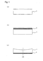
- a disk-shaped metal plate (conductor plate) 1 which was composed of an aluminum alloy having a diameter of 150 mm and a thickness of 15 mm, was formed.
- One surface of the metal plate 1 was polished to be flat so that the flatness was about several to several tens of ⁇ m.
- a nickel film 3 was formed to have a thickness of about several tens of ⁇ m to several mm on the flat surface with the electroless plating method (Fig. 1(b)).
- the plated surface 3 was ground or cut by using a grinding machining machine or a cutting machining machine (not shown), and thus the plating thickness was made uniform.
- the surface which was disposed on the side opposite to the surface having the nickel film 3 formed thereon, was machined to be a concave surface having a radius of curvature of 1800 mm by using a lathe (not shown) so that the thickness is thinnest at the central axis AX of the metal plate 1 (Fig. 1(c)).
- the thickness of the metal plate 1 at the central axis AX was 9.95 mm.
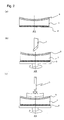
- a nickel film 5 having a thickness of 100 ⁇ m was formed on the concave surface with the electroless plating method (Fig. 2(a)). Further, the nickel film 5 was subjected to cutting in an amount of 50 ⁇ m by using an NC cutting machine 7 provided with a diamond turning tool (Fig. 2(b)). Accordingly, the thickness was 10 mm at the central axis AX of the reflecting mirror element. The surface roughness of the nickel film 5 after the cutting was not more than 1 ⁇ m.
- the nickel film 5, which was disposed on the disk-shaped metal plate 1 was polished by using an Oscar polishing machine 9.
- the polishing was performed so that the surface roughness Rrms ⁇ 0.3 nm was satisfied while maintaining the radius of curvature 1800 mm.
- a reflecting mirror element 10 was obtained, in which the length was 15.0 mm, the width was 1.0 mm, and the radii of curvature of the convex surface and the concave surface were 20 mm respectively.
- the circular arc-shaped reflecting mirror elements were cut out from the metal plate 1', they were cut out with three different patterns of A, B, C as shown in Figs. 4(a), 4(b), and 4(c) respectively. That is, in Fig. 4(a), the center of the circular arc-shaped plane pattern A is positioned while being deviated by +Zh in the Z direction from the center AX of the metal plate 1'.
- Fig. 4(a) the center of the circular arc-shaped plane pattern A is positioned while being deviated by +Zh in the Z direction from the center AX of the metal plate 1'.
- the center of the circular arc-shaped plane pattern B is positioned while being deviated by +Zh in the Z direction and -Yh in the Y direction from the center AX of the metal plate 1'.
- the center of the circular arc-shaped plane pattern is positioned while being deviated by +Zh in the Z direction and +Yh in the Y direction from the center AX of the metal plate 1'.
- the reflecting mirror elements, which were cut out in accordance with the respective patterns (positions) of A, B, C, were mutually different from each other in the curved surface shape of the upper surface respectively.
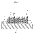
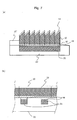
- the cut out reflecting mirror elements 10 are arranged in a predetermined order on a base plate 13 as shown in Fig. 5.
- the base plate 13 is composed of a neodymium magnet having a diameter of 100 mm, a height of 10 mm, and a flatness (surface roughness) of 5 ⁇ m.
- the neodymium magnet sometimes becomes rusty. Therefore, a nickel plating having a thickness of 2 to 3 ⁇ m, which serves as a rust preventive, may be applied to the surface.
- positioning guides 15, which fasten the reflecting mirror elements are provided at five places at outer circumferential portions of the base plate 13.
- the reflecting mirror elements 10 were arranged on the base plate 13 so that the nickel films 17 (portions cut out from the nickel film 3) were magnetically joined to the base plate 13.
- the reflecting mirror element 10a is firstly arranged on the base plate 13 so that the reflecting mirror element 10a is pushed against the guide 15. Accordingly, the reflecting mirror element 10a is positioned on the surface of the base plate 13.
- the reflecting mirror element 10b is arranged on the base plate 13 so that the reflecting mirror element 10b is pushed against the reflecting mirror element 10a.
- the reflecting mirror elements are successively arranged so that they are adjoined to one another. Accordingly, the reflecting mirror elements are positioned on the base plate 13 highly accurately without any gap.
- the reflecting mirror elements have the three types of the curved surface shapes (corresponding to the patterns A, B, C) which are different from each other as described above.
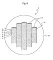
- the reflecting mirror elements were arranged, for example, in accordance with an arrangement order as shown in Fig. 6 so that the concave-shaped nickel films 19 (portions cut out from the nickel film 5, hereinafter referred to as "reflecting surfaces") were directed in an identical direction.
- the reflecting mirror elements 10, which are arranged on the base plate 13, can be also positionally adjusted and arranged highly accurately, because the flatness of the base plate 13 is high. Accordingly, a multifaceted reflecting mirror 2 was obtained as shown in Fig. 6.
- a means for cooling the base plate 13 may be provided.
- the first modified embodiment was constructed in the same manner as the first embodiment except that a base plate 20 was formed of a non-magnetic metal, recesses 18 each having a rectangular cross section were provided in the base plate 20, and magnets 21 for fixing the reflecting mirror elements 10 were embedded in the recesses 18.
- the base plate 20 was manufactured with a non-magnetic metal material composed of brass to have the same size as that in the first embodiment.
- the plurality of recesses 18 are formed in parallel in a predetermined direction on one surface of the base plate 20 by using an NC cutting machine (not shown) so that the cross section is rectangular with a length of 100 mm, a width of 3.0 mm, and a depth of 10 mm.
- the neodymium magnet sometimes becomes rusty. Therefore, a nickel plating having a thickness of 2 to 3 ⁇ m, which serves as a rust preventive, may be applied to the surface.
- the depth ranging from the base plate surface to the magnet 21 was 0.5 mm.
- the reflecting mirror element 10 was arranged on the base plate 20 so that the reflecting mirror element 10 rode over the two recesses 18.
- the surface of the base plate 20 is made of the non-magnetic metal. Therefore, the flatness is high and the surface roughness is small, as compared with a case of formation with a magnetic member as a sintered body. Accordingly, the respective reflecting mirror elements 10 can be installed on the base plate 20 highly accurately especially in relation to the position in the height direction. That is, it is possible to enhance the uniformity of the position in the height direction of the reflecting surface of the multifaceted reflecting mirror. Further, the magnets 21 are not exposed to the surface of the base plate 20, and no contact is made between the magnets 21 and the reflecting mirror elements 10.
- the magnets 21 are prevented from direct heat transfer from the reflecting mirror elements 10. Therefore, it is possible for the magnets 21 to maintain the magnetization (magnetic field) for supporting the reflecting mirror elements 10 on the base plate 20. Further, even when the flatness is lowered by the nickel plating applied to the magnets, the arrangement accuracy of the reflecting mirror elements 10 is not affected, because no contact is made between the magnets 21 and the reflecting mirror elements 10.
- the size of the magnet to be used in this modified embodiment is smaller than the size of the magnet to be used in the first embodiment. Therefore, it is easy to perform the manufacturing process.
- Reflecting mirror elements 10' were constructed in the same manner as in the first embodiment except that silicon was used in place of the aluminum alloy as the material for the metal plate 1 and the nickel film 5 based on the electroless plating was not formed.
- One having a low resistance value (resistance value: 0.02 ⁇ m) was used as silicon.
- the surface of the reflecting mirror element 10' can be made into a mirror surface by polishing the surface of silicon by using an Oscar polishing machine. Therefore, it is unnecessary to perform the electroless plating step which would be otherwise performed in order to form the reflecting surface of the reflecting mirror element. It is possible to simplify the production steps for the reflecting mirror element.
- Reflecting mirror elements in the second embodiment were basically constructed in the same manner as in the first embodiment except that invar was used as a material for a metal plate 1.
- the adjoining reflecting mirror elements are magnetized to have an identical polarity, because the side of the reflecting mirror element, which is disposed on the contact surface (bottom surface) with respect to the base plate, is magnetized to have a magnetic pole opposite to that of the base plate. Therefore, the adjoining reflecting mirror elements are consequently repelled to one another.
- the repulsive force between the adjoining reflecting mirror elements is small, because the nickel film 17 as the magnetic material is a thin film.
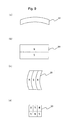
- the repulsive force is relatively large, because the reflecting mirror element itself is composed of invar which is a magnetic material. Therefore, the repulsive force makes it impossible to arrange the plurality of reflecting mirror elements in accordance with a predetermined pattern on the base plate while effecting tight contact with each other. Accordingly, as explained below, magnets are installed between the base plate and the reflecting mirror elements respectively. As shown in Figs. 9(a) and 9(b), neodymium magnets 23, each of which had a circular arc-shaped cross section in the same manner as the cut out shape of the reflecting mirror element, were manufactured.
- the magnets 23 were bonded to one another so that the magnetic poles were disposed alternately beforehand.
- a group of bonded magnets 23 were installed on a surface plate 25 composed of nickel.
- the reflecting mirror elements 10" were successively arranged so that one reflecting mirror element 10" was positioned on each of the plurality of arranged magnets 23. In this procedure, guides 15" are provided on the surface plate. Therefore, the reflecting mirror elements 10" can be successively arranged on the basis of the guides 15".
- the respective reflecting mirror elements 10" made of invar are magnetically jointed to the magnets 23 on which they are seated.
- the adjoining magnets 23 have the mutually opposite polarities, and hence the adjoining reflecting mirror elements 10" are mutually magnetized so that the opposite polarities are formed as well. Therefore, the adjoining reflecting mirror elements 10" are not repelled to one another, and they make tight contact in accordance with the opposite polarities. Thus, their positions are reliably fixed.
- a third embodiment of the present invention will be explained with reference to Figs. 12 and 13.
- a multifaceted reflecting mirror was constructed in the same manner as in the first embodiment except that reflecting mirror elements were formed of magnet, and a base plate made of metal was used. Ferrite was used as a metal plate 1 from which the reflecting mirror elements were cut out.
- the reflecting mirror elements 30 were cut out by using a wire electric discharge machining machine from the disk-shaped metal plate 1 made of ferrite in the same manner as in the first embodiment.
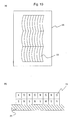
- the respective reflecting mirror elements 30 were magnetized by using an electromagnet. In this procedure, the reflecting mirror elements 30 were magnetized so that the adjoining reflecting mirror elements 30 had mutually different polarities on the reflecting surface side and on the seating surface side respectively as shown in Fig. 12(b).
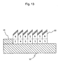
- the magnetized reflecting mirror elements 30 were bonded to one another with the magnetic force as shown in Figs. 12(a) and 12(b). Subsequently, as shown in Fig. 13, a group of reflecting mirror elements 30, which had been bonded to one another with the magnetic force, were adhered onto a base plate 13' composed of nickel. In this procedure, the reflecting mirror elements 30 were positionally adjusted by using guides 16 provided on the base plate 13' in the same manner as in the first embodiment. Accordingly, it is possible to obtain the multifaceted reflecting mirror having been positionally adjusted highly accurately.
- the respective reflecting mirror elements were magnetized after being cut out from the metal plate 1.
- the following procedure may be adopted. That is, metal plates 1 made of ferrite are previously prepared, and they are magnetized so that different magnetic poles appear mutually on reflecting surface sides. Reflecting mirror elements, which are cut out from each of the metal plates 1, are combined and arranged on the base plate. Further, the multifaceted reflecting mirror as described above may be installed with a cooling unit for cooling the reflecting mirror elements in order to avoid the decrease in coercive force of the magnet which would be otherwise caused by the heat generated in the reflecting mirror elements by being irradiated with the light.
- the multifaceted reflecting mirror is installed in vacuum. Therefore, a contact type cooling unit such as a Peltier element may be provided on the back surface of the multifaceted reflecting mirror, i.e., on the side of the base plate. A flow passage may be provided in the base plate, and cooling water may be allowed to flow through the flow passage to cool the reflecting mirror elements.
- a contact type cooling unit such as a Peltier element may be provided on the back surface of the multifaceted reflecting mirror, i.e., on the side of the base plate.
- a flow passage may be provided in the base plate, and cooling water may be allowed to flow through the flow passage to cool the reflecting mirror elements.
- the aluminum alloy was used as the material for the reflecting mirror element.
- steel lumber, oxygen-free copper, or super invar may be used.
- the electric discharge machining can be performed when a conductive material is used, and hence it is easy to cut out the reflecting mirror element having a desired shape from a metal plate.
- the electroless nickel plating was applied to invar.
- a thin film having high reflectivity such as those of nickel alloy may be formed in place of the electroless nickel plating, provided that the mirror surface performance is satisfactory after the cutting and the polishing.
- glass it is also possible to use another material for the reflecting mirror element.
- Those usable as the glass include, for example, quartz glass and low expansion glass.
- the cutting machining can be performed in place of the wire electric discharge machining in order to cut out the glass piece from the substrate.
- the wire electric discharge machining machine was used to cut out the reflecting mirror element.
- the reflecting mirror element may be cut out with the milling.
- the permanent magnet was used as the magnet for constructing the base plate.
- an electromagnet may be embedded in the base plate, or it may be attached to the base plate.
- the reflecting mirror elements, which were cut from the disk-shaped metal plate had three types of patterns, i.e., patterns A, B, C. However, there is no special limitation to the three type. The number of patterns may be either larger than three or smaller than three. Further, all of the reflecting mirror elements may have an identical reflecting surface shape, or the reflecting mirror elements may have different reflecting surface shapes.
- the reflecting mirror element may be obtained by cutting off a part of an aspheric surface.
- the reflecting mirror elements having different shapes may be arranged in accordance with a predetermined repeating arrangement, or they may be arranged in other ways.
- the size of the multifaceted reflecting mirror and the size of the reflecting mirror element are not limited to those described in the embodiments of the present invention as well. Further, the total number of basic reflecting mirrors is not limited to those described in the embodiments of the present invention as well. The sizes and the number as described above may be arbitrarily changed depending on the optical design of the multifaceted reflecting mirror.
- an aluminum thin film may be formed to have a thickness of about 100 nm with the vapor deposition on the reflecting surface of the reflecting mirror element in order to improve the reflectance
- a film of MgF 2 may be formed to have a thickness of several tens of nm with the vapor deposition thereon in order to prevent the oxidation and maintain the reflectance.
- an alternate multilayered film comprising 40 to 50 layers of laminated two-layered films each having a thickness of 7 nm and composed of Si (4.6 nm) and Mo (2.4 nm).
- positioning guides were provided at the outer circumferential portions or the edge portions of the base plate.
- positioning guides 16' may be provided in the arrays of the reflecting mirror elements 10 at constant intervals as shown in Fig. 14. Accordingly, it is possible to perform the positional adjustment of the reflecting mirror elements with a higher degree of accuracy.
- a second multifaceted reflecting mirror was constructed in the same manner as in the first embodiment except that reflecting mirror elements 12 were cut out to have rectangular shapes (shapes of the patterns A, B, C in Fig.
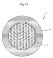
- the first multifaceted reflecting mirror 2 as shown in Fig. 6 and the second multifaceted reflecting mirror 2' as shown in Fig. 15 were obtained.
- the multifaceted reflecting mirrors were combined and arranged at predetermined positions. Accordingly, the light beams, which are reflected by the respective reflecting mirror elements 10 of the first multifaceted reflecting mirror 2, come into the corresponding respective reflecting mirror elements 12 of the second multifaceted reflecting mirror 2'.
- the reflected light beams from the respective reflecting mirror elements 12 are converged into an identical area by using, for example, a condenser lens. Accordingly, it is possible to generate an illumination area having a uniform illuminance distribution in the area.
- An illumination light beam in the short wavelength region, which causes the light absorption by the lens, is used for the optical system obtained by combining the multifaceted reflecting mirrors as described above.
- Such an optical system is useful for various ways of use which require a uniform illuminance distribution in the illumination area.
- such an optical system is preferably used for an illuminating apparatus for an exposure apparatus for producing semiconductors and liquid crystal boards by utilizing the light in the soft X-ray region.
- FIG. 17 shows a schematic view illustrating a projection exposure apparatus 120 according to the present invention.
- Gas of Xe or liquid of Xe is spouted from a gas nozzle 102.
- a YAG laser which is radiated from a laser light source 100, is radiated thereon via a light-collecting lens 101 to generate the plasma.
- a substance containing Sn (stannum) may be arranged or spouted at the position of the focusing point 103 of the laser, and the YAG laser may be radiated thereon to generate a soft X-ray.
- the light beams, which come into respective reflecting mirror elements of the first multifaceted reflecting mirror 106', are reflected by reflecting surfaces of the reflecting mirror elements respectively, and they come into corresponding reflecting mirror elements of a second multifaceted reflecting mirror 106".
- the light beam, which is reflected by the second multifaceted reflecting mirror 106" passes along a condenser optical element 107' and a reflecting mirror 107", and it radiates only a predetermined area on a mask 108 held on a mask stage (not shown).
- a circuit pattern to be transferred onto a wafer is previously formed as a reflector pattern on the mask 108 with the photolithography technique.
- the light beam which is reflected in accordance with the circuit pattern on the mask 108, is radiated onto the surface of the wafer 110 via a reflection type projection optical apparatus 109.
- the mask 108 and the wafer 110 are relatively moved while being synchronized with each other by using the unillustrated mask stage and the unillustrated wafer stage respectively.
- the entire circuit pattern on the mask 108 is scanned with the illumination light beam. Therefore, the entire circuit pattern can be transferred onto the wafer 110.
- the movement velocities of the mask 108 and the wafer 110 are controlled by controlling the mask stage and the wafer stage by using an unillustrated mask stage controller and an unillustrated wafer stage controller respectively, while the positions of the mask stage and the wafer stage are measured by using laser distance interferometers respectively.
- Main components of the exposure apparatus 120 are accommodated in a chamber 130 as shown in Fig. 17.
- the pressure in the chamber 130 is reduced by an unillustrated pressure-reducing unit to give a state of reduced pressure (vacuum) of about 10 -4 to 10 -7 Torr.
- the reduced pressure atmosphere avoids any decrease in illuminance of the illumination light beam at the mask position and the wafer position, which would be otherwise caused by the absorption of light effected by gas molecules.
- the area which includes the gas nozzle 102, the laser-focusing point 103, and the reflecting mirror 104, is surrounded by the chamber, and a hole is bored through only a portion through which the light flux passes. A duct to aspirate the gas spouted from the gas nozzle 102 is provided. Owing to this arrangement, it is possible to maintain a high degree of vacuum in the chamber.
- the multifaceted reflecting mirror which was manufactured in accordance with the first embodiment, was used as the first multifaceted reflecting mirror. However, it is needless to say that those based on the other embodiments or the modified embodiments thereof may be used. Especially, the multifaceted reflecting mirror manufactured in accordance with the first embodiment has the following advantage.
- the multifaceted reflecting mirror can be installed with the magnetic force in the chamber of the exposure apparatus or on the support stand of the illumination optical system, because the base plate is composed of the magnet. Therefore, such a multifaceted reflecting mirror is extremely advantageous to adjust the optical path of the illumination optical system and perform the maintenance for the multifaceted reflecting mirror. Details of such an exposure apparatus are disclosed, for example, in United States Patent No. 5,581,605. The disclosure of the United States Patent is incorporated herein by reference within a range of permission of the laws and ordinances of the designated state or the selected state designated or selected in this international application.
- the multifaceted reflecting mirror which is provided with the reflecting mirror elements, can be easily manufactured with a high degree of positional accuracy by arranging the reflecting mirror elements on the base plate with the magnetic force.
- the illuminating apparatus in which the multifaceted reflecting mirror of the present invention is incorporated, is used, it is possible to effect the uniform illumination and the uniform exposure.
- the exposure apparatus which is based on the use of the illuminating apparatus according to the present invention, makes it possible to improve the optical characteristics and realize the high throughput brought about by shortening the exposure time.
- the exposure apparatus which is provided with the multifaceted reflecting mirror of the present invention constructed by using no adhesive, is extremely useful to perform the exposure of the circuit pattern having the narrow line width.
Landscapes
- Physics & Mathematics (AREA)
- General Physics & Mathematics (AREA)
- Optics & Photonics (AREA)
- Engineering & Computer Science (AREA)
- Health & Medical Sciences (AREA)
- Public Health (AREA)
- Epidemiology (AREA)
- Environmental & Geological Engineering (AREA)
- Spectroscopy & Molecular Physics (AREA)
- High Energy & Nuclear Physics (AREA)
- General Engineering & Computer Science (AREA)
- Electromagnetism (AREA)
- Exposure And Positioning Against Photoresist Photosensitive Materials (AREA)
- Optical Elements Other Than Lenses (AREA)
- Microscoopes, Condenser (AREA)
- Exposure Of Semiconductors, Excluding Electron Or Ion Beam Exposure (AREA)
Abstract
Description
Subsequently, the reflecting
Claims (28)
- A multifaceted reflecting mirror comprising:a plurality of reflecting mirror elements each of which is provided with a reflecting surface; anda placement plate which is joined to the reflecting mirror elements with magnetic force, wherein:the reflecting mirror elements are arranged adjacently on the placement plate.
- The multifaceted reflecting mirror according to claim 1, further comprising, on the placement plate, a positioning member which positions at least one of the reflecting mirror elements on the placement plate.
- The multifaceted reflecting mirror according to claim 1, wherein the placement plate includes a magnet.
- The multifaceted reflecting mirror according to claim 3, wherein a magnetic film is formed on a bottom surface of each of the reflecting mirror elements.
- The multifaceted reflecting mirror according to claim 3, wherein a magnet is embedded in the placement plate.
- The multifaceted reflecting mirror according to claim 5, wherein a plurality of recesses are formed at predetermined intervals in the placement plate, and the magnet is accommodated in each of the recesses so that the magnet is not exposed to a surface of the placement plate.
- The multifaceted reflecting mirror according to claim 3, wherein each of the reflecting mirror elements is composed of a magnetic material, magnetic elements are provided between the placement plate and the respective reflecting mirror elements, and the magnetic elements are arranged on the placement plate so that polarities of the adjoining magnetic elements are opposite to one another.
- The multifaceted reflecting mirror according to claim 1, wherein each of the reflecting mirror elements includes a magnet.
- The multifaceted reflecting mirror according to any one of claims 1 to 8, wherein each of the reflecting mirror elements is formed of a conductor.
- The multifaceted reflecting mirror according to any one of claims 1 to 8, wherein a metal plating is applied to the reflecting surface of each of the reflecting mirror elements.
- An illumination optical system comprising:a first multifaceted reflecting mirror which comprises a plurality of reflecting mirror elements having reflecting surfaces, the plurality of reflecting mirror elements being disposed adjacently on a first placement plate; anda second multifaceted reflecting mirror which comprises a plurality of reflecting mirror elements having reflecting surfaces, the plurality of reflecting mirror elements being disposed adjacently on a second placement plate, wherein:the respective reflecting mirror elements of the first multifaceted reflecting mirror are fixed on the first placement plate with magnetic force.
- The illumination optical system according to claim 11, wherein the respective reflecting mirror elements of the second multifaceted reflecting mirror are fixed on the second placement plate with magnetic force.
- The illumination optical system according to claim 12, wherein the reflecting surface of each of the reflecting mirror elements of the first multifaceted reflecting mirror is circular arc-shaped, and the reflecting surface of each of the reflecting mirror elements of the second multifaceted reflecting mirror is rectangular.
- The illumination optical system according to claim 11, wherein the first placement plate includes a magnet.
- The illumination optical system according to claim 14, wherein a magnetic film is formed on a bottom surface of each of the reflecting mirror elements of the first multifaceted reflecting mirror.
- The illumination optical system according to claim 14, wherein a magnet is embedded in the first placement plate.
- The illumination optical system according to claim 14, wherein each of the reflecting mirror elements of the first multifaceted reflecting mirror is composed of a magnetic material, a magnetic element is provided between the first placement plate and each of the reflecting mirror elements of the first multifaceted reflecting mirror, and the magnetic elements are arranged so that polarities of the adjoining magnetic elements are opposite to one another.
- The illumination optical system according to claim 11, wherein each of the reflecting mirror elements of the first multifaceted reflecting mirror includes a magnet.
- The illumination optical system according to any one of claims 11 to 18, further comprising, on the first placement plate, a positioning member which determines a position of at least one of the reflecting mirror elements on the first placement plate.
- The illumination optical system according to any one of claims 11 to 18, wherein each of the reflecting mirror elements of the first multifaceted reflecting mirror and the second multifaceted reflecting mirror is formed of a conductor.
- An exposure apparatus comprising the illumination optical system as defined in claim 11, wherein a substrate is exposed with a mask pattern.
- The exposure apparatus according to claim 21, wherein a light beam, which is supplied to the illumination optical system, has a wavelength of not more than 200 nm.
- The exposure apparatus according to claim 22, wherein an atmosphere, in which the illumination optical system in the exposure apparatus is accommodated, is vacuum.
- The exposure apparatus according to claim 22, further comprising a reflection type projection optical system which projects, onto the substrate, an image of the mask pattern illuminated by the illumination optical system.
- The exposure apparatus, wherein the reflecting surface of the reflecting mirror element of the first multifaceted reflecting mirror has a shape which is similar to a shape of an optical field of the reflection type projection optical system.
- A method for producing the multifaceted reflecting mirror as defined in claim 1, comprising:forming a reflecting surface on a conductor plate;cutting out a plurality of reflecting mirror elements from the conductor plate with electric discharge machining; andarranging the reflecting mirror elements on a placement plate which is joined to the reflecting mirror elements with magnetic force so that the reflecting mirror elements are arranged mutually adjacently in accordance with a predetermined pattern.
- The method for producing the multifaceted reflecting mirror according to claim 26, further comprising providing a positioning member on the placement plate, wherein at least one of the reflecting mirror elements is pushed against the positioning member to position the reflecting mirror element on the placement plate.
- The method for producing the multifaceted reflecting mirror according to claim 26, further comprising forming a magnetic film on a bottom surface of the cut out reflecting mirror element.
Applications Claiming Priority (5)
| Application Number | Priority Date | Filing Date | Title |
|---|---|---|---|
| JP2001047679 | 2001-02-23 | ||
| JP2001047680 | 2001-02-23 | ||
| JP2001047680 | 2001-02-23 | ||
| JP2001047679 | 2001-02-23 | ||
| PCT/JP2002/001614 WO2002067021A1 (en) | 2001-02-23 | 2002-02-22 | Polygon reflector, and illumination optical system and semiconductor exposure device using the polygon reflector |
Publications (2)
| Publication Number | Publication Date |
|---|---|
| EP1296162A1 true EP1296162A1 (en) | 2003-03-26 |
| EP1296162A4 EP1296162A4 (en) | 2007-02-28 |
Family
ID=26609951
Family Applications (1)
| Application Number | Title | Priority Date | Filing Date |
|---|---|---|---|
| EP02700713A Withdrawn EP1296162A4 (en) | 2001-02-23 | 2002-02-22 | Polygon reflector, and illumination optical system and semiconductor exposure device using the polygon reflector |
Country Status (5)
| Country | Link |
|---|---|
| US (1) | US6984051B2 (en) |
| EP (1) | EP1296162A4 (en) |
| JP (1) | JP4196676B2 (en) |
| TW (1) | TW569040B (en) |
| WO (1) | WO2002067021A1 (en) |
Cited By (3)
| Publication number | Priority date | Publication date | Assignee | Title |
|---|---|---|---|---|
| WO2005006081A1 (en) * | 2003-07-09 | 2005-01-20 | Carl-Zeiss Smt Ag | Facet mirrors and a method for producing mirror facets |
| WO2008101656A3 (en) * | 2007-02-19 | 2009-03-12 | Zeiss Carl Smt Ag | Method for producing facet mirrors and projection exposure apparatus |
| EP3611497A1 (en) * | 2018-08-13 | 2020-02-19 | Komax Holding Ag | Inspection apparatus for inspecting a cable tip of a cable and method for cleaning the mirror of an inspection apparatus |
Families Citing this family (18)
| Publication number | Priority date | Publication date | Assignee | Title |
|---|---|---|---|---|
| US7843632B2 (en) * | 2006-08-16 | 2010-11-30 | Cymer, Inc. | EUV optics |
| US7404647B1 (en) * | 2003-12-11 | 2008-07-29 | Gsi Group Corporation | Method for optimal material selection and processing for dynamic mirror applications |
| DE102005028456A1 (en) * | 2005-06-17 | 2006-12-28 | Schott Ag | Metal reflector and method for its production |
| US7303612B2 (en) * | 2005-03-24 | 2007-12-04 | L2B Environmental Systems Inc. | UV reflective cavity and method of providing same |
| EP1950594A1 (en) | 2007-01-17 | 2008-07-30 | Carl Zeiss SMT AG | Imaging optical system, projection illumination unit for microlithography with such an optical system, method for manufacturing a microstructured component with such a projection illumination unit, microstructured component produced by the manufacturing method and use of such an optical system |
| DE102008040938A1 (en) | 2007-08-16 | 2009-02-19 | Carl Zeiss Smt Ag | Panel facet's optical surface producing method for microlithography projector, involves adjusting tilting angle at longitudinal axis or tilting angle at transverse axis at facet base bodies in predetermined range |
| US8130904B2 (en) * | 2009-01-29 | 2012-03-06 | The Invention Science Fund I, Llc | Diagnostic delivery service |
| US8041008B2 (en) * | 2009-01-29 | 2011-10-18 | The Invention Science Fund I, Llc | Diagnostic delivery service |
| JP5428375B2 (en) * | 2009-02-18 | 2014-02-26 | 株式会社ニコン | Holding apparatus, optical system, exposure apparatus, and device manufacturing method |
| US8575576B2 (en) * | 2011-02-14 | 2013-11-05 | Kla-Tencor Corporation | Optical imaging system with laser droplet plasma illuminator |
| CN102507494A (en) * | 2011-11-02 | 2012-06-20 | 太原理工大学 | Long-optical-path and light-intensity-adjustable infrared methane gas sensor |
| DE102015209175A1 (en) * | 2015-05-20 | 2016-11-24 | Carl Zeiss Smt Gmbh | Pupil facet mirror |
| DE102015120853B3 (en) * | 2015-12-01 | 2017-04-27 | Friedrich-Schiller-Universität Jena | Method and device for producing an optical component having at least three monolithically arranged optical functional surfaces and optical component |
| CN108873117B (en) * | 2017-05-16 | 2020-04-21 | 昇印光电(昆山)股份有限公司 | Optical components, mobile phone covers and molds for preparing optical components |
| KR102387821B1 (en) * | 2017-06-01 | 2022-04-15 | 가부시키가이샤 아스카넷토 | Method for manufacturing a stereoscopic image forming apparatus and a stereoscopic image forming apparatus |
| US11042097B1 (en) * | 2019-12-31 | 2021-06-22 | Soulnano Limited | Multi-mirror UV-LED optical lithography system |
| US12517347B2 (en) * | 2021-04-16 | 2026-01-06 | Corning Incorporated | Polygon mirror |
| US20240168206A1 (en) * | 2022-11-17 | 2024-05-23 | Innovusion, Inc. | Systems and methods for polygon mirror angles adjustment |
Family Cites Families (10)
| Publication number | Priority date | Publication date | Assignee | Title |
|---|---|---|---|---|
| JPS5241538A (en) * | 1975-05-14 | 1977-03-31 | Nec Corp | Device for supporting a reflecting mirror |
| US4456332A (en) * | 1980-04-07 | 1984-06-26 | Atlantic Richfield Company | Method of forming structural heliostat |
| JPS60232552A (en) | 1984-05-02 | 1985-11-19 | Canon Inc | Lighting optical system |
| JP2673517B2 (en) | 1987-06-15 | 1997-11-05 | キヤノン株式会社 | Exposure equipment |
| US4906087A (en) * | 1989-06-16 | 1990-03-06 | Litton Systems, Inc. | Magneto-retractive deformable mirror |
| US5204731A (en) * | 1989-12-04 | 1993-04-20 | Sokkisha Co., Ltd. | Method and apparatus for measuring the coordinates of a surveyed point |
| US5347402A (en) * | 1992-08-12 | 1994-09-13 | Porter Arbogast | Multiple mirror assembly for solar collector |
| JP4238390B2 (en) * | 1998-02-27 | 2009-03-18 | 株式会社ニコン | LIGHTING APPARATUS, EXPOSURE APPARATUS PROVIDED WITH THE ILLUMINATION APPARATUS, AND METHOD FOR MANUFACTURING SEMICONDUCTOR DEVICE USING THE EXPOSURE APPARATUS |
| JP2000098114A (en) * | 1998-09-22 | 2000-04-07 | Nikon Corp | Method for manufacturing reflector formed with multiple light sources and optical device using the reflector |
| JP2000162415A (en) | 1998-09-22 | 2000-06-16 | Nikon Corp | Method for manufacturing a reflecting mirror, reflection type illumination device, or semiconductor exposure device |
-
2002
- 2002-02-22 EP EP02700713A patent/EP1296162A4/en not_active Withdrawn
- 2002-02-22 WO PCT/JP2002/001614 patent/WO2002067021A1/en not_active Ceased
- 2002-02-22 TW TW091103100A patent/TW569040B/en active
- 2002-02-22 JP JP2002566692A patent/JP4196676B2/en not_active Expired - Fee Related
- 2002-11-06 US US10/288,337 patent/US6984051B2/en not_active Expired - Lifetime
Cited By (4)
| Publication number | Priority date | Publication date | Assignee | Title |
|---|---|---|---|---|
| WO2005006081A1 (en) * | 2003-07-09 | 2005-01-20 | Carl-Zeiss Smt Ag | Facet mirrors and a method for producing mirror facets |
| WO2008101656A3 (en) * | 2007-02-19 | 2009-03-12 | Zeiss Carl Smt Ag | Method for producing facet mirrors and projection exposure apparatus |
| EP3611497A1 (en) * | 2018-08-13 | 2020-02-19 | Komax Holding Ag | Inspection apparatus for inspecting a cable tip of a cable and method for cleaning the mirror of an inspection apparatus |
| US11231559B2 (en) | 2018-08-13 | 2022-01-25 | Komax Holding Ag | Inspection device for inspecting a cable end of a cable and a method for cleaning |
Also Published As
| Publication number | Publication date |
|---|---|
| US6984051B2 (en) | 2006-01-10 |
| WO2002067021A1 (en) | 2002-08-29 |
| JP4196676B2 (en) | 2008-12-17 |
| EP1296162A4 (en) | 2007-02-28 |
| TW569040B (en) | 2004-01-01 |
| US20030058555A1 (en) | 2003-03-27 |
| JPWO2002067021A1 (en) | 2004-06-24 |
Similar Documents
| Publication | Publication Date | Title |
|---|---|---|
| US6984051B2 (en) | Multifaceted reflecting mirror, illumination optical system based on use of the same, and semiconductor exposure apparatus | |
| US6594334B1 (en) | Exposure method and exposure apparatus | |
| US6144119A (en) | Planar electric motor with dual coil and magnet arrays | |
| KR100548714B1 (en) | Lithographic apparatus and motors for the apparatus | |
| USRE41681E1 (en) | Enhanced illuminator for use in photolithographic systems | |
| US20020149270A1 (en) | Planar electric motor with two sided magnet array | |
| US7898119B2 (en) | Planar motor and stage using the same | |
| US6526118B2 (en) | Projection exposure apparatus and method, and illumination optical system thereof | |
| JP5140268B2 (en) | Magnet assembly, linear actuator, planar motor, and lithographic apparatus | |
| JP2015532825A (en) | Electromagnetic actuator, support, and lithographic apparatus | |
| JP5214771B2 (en) | Lithographic apparatus and lithographic apparatus cooling method | |
| KR20160124857A (en) | Method for illuminating an object field of a projection exposure system | |
| KR100632878B1 (en) | Lithographic Apparatus, Device Manufacturing Method, and Device Manufactured Thereby | |
| US20030213889A1 (en) | Non-contacting holding devices for an optical component, and optical systems and lithographic exposure systems comprising same | |
| US6335786B1 (en) | Exposure apparatus | |
| JP2009266886A (en) | Mask, mask holder, photolithography machine, and manufacturing method of device | |
| JP2000286191A (en) | Exposure apparatus, exposure method, and device manufacturing method | |
| JP4599334B2 (en) | Method for manufacturing article support member | |
| KR100585467B1 (en) | Substrate carrier and method for making a substrate carrier | |
| JP2014154698A (en) | Optical device, illuminating device, exposure device, method of manufacturing device, and holding method of optical element | |
| JP2010192674A (en) | Holding device, optical system, exposure device, and method for manufacturing device | |
| JP2000098114A (en) | Method for manufacturing reflector formed with multiple light sources and optical device using the reflector | |
| US9323157B2 (en) | Mirror assembly for an exposure apparatus | |
| JP2002131520A (en) | Manufacturing method of polyhedral mirror and exposure apparatus using the mirror | |
| JP2014160700A (en) | Optical device, lighting device, exposure device, device manufacturing method, and holding method of optical element |
Legal Events
| Date | Code | Title | Description |
|---|---|---|---|
| PUAI | Public reference made under article 153(3) epc to a published international application that has entered the european phase |
Free format text: ORIGINAL CODE: 0009012 |
|
| AK | Designated contracting states |
Kind code of ref document: A1 Designated state(s): AT BE CH CY DE DK ES FI FR GB GR IE IT LI LU MC NL PT SE TR Designated state(s): AT BE CH CY DE DK ES FI FR GB GR IE IT LI LU MC NL PT SE TR |
|
| AX | Request for extension of the european patent |
Extension state: AL LT LV MK RO SI |
|
| 17P | Request for examination filed |
Effective date: 20030220 |
|
| A4 | Supplementary search report drawn up and despatched |
Effective date: 20070126 |
|
| RIC1 | Information provided on ipc code assigned before grant |
Ipc: G03F 7/20 20060101ALI20070122BHEP Ipc: G02B 5/09 20060101AFI20070122BHEP |
|
| 17Q | First examination report despatched |
Effective date: 20070413 |
|
| STAA | Information on the status of an ep patent application or granted ep patent |
Free format text: STATUS: THE APPLICATION IS DEEMED TO BE WITHDRAWN |
|
| 18D | Application deemed to be withdrawn |
Effective date: 20081231 |