EP1294089A2 - Remodulation of an RF carrier modulated signal - Google Patents
Remodulation of an RF carrier modulated signal Download PDFInfo
- Publication number
- EP1294089A2 EP1294089A2 EP02019639A EP02019639A EP1294089A2 EP 1294089 A2 EP1294089 A2 EP 1294089A2 EP 02019639 A EP02019639 A EP 02019639A EP 02019639 A EP02019639 A EP 02019639A EP 1294089 A2 EP1294089 A2 EP 1294089A2
- Authority
- EP
- European Patent Office
- Prior art keywords
- frequency
- modulated signal
- carrier
- carrier modulated
- modulating
- Prior art date
- Legal status (The legal status is an assumption and is not a legal conclusion. Google has not performed a legal analysis and makes no representation as to the accuracy of the status listed.)
- Withdrawn
Links
Images
Classifications
-
- H—ELECTRICITY
- H03—ELECTRONIC CIRCUITRY
- H03K—PULSE TECHNIQUE
- H03K7/00—Modulating pulses with a continuously-variable modulating signal
-
- H—ELECTRICITY
- H03—ELECTRONIC CIRCUITRY
- H03D—DEMODULATION OR TRANSFERENCE OF MODULATION FROM ONE CARRIER TO ANOTHER
- H03D7/00—Transference of modulation from one carrier to another, e.g. frequency-changing
- H03D7/16—Multiple-frequency-changing
Definitions
- the present invention relates to modulating apparatus and method for an radio frequency (RF) carrier signal.
- RF radio frequency
- Up-converting and down-converting radio frequency (RF) carrier modulated signals is a common practice that is used in RF receivers and transmitters. Such up-converting and down-converting requires the RF carrier modulated signal to be re-modulated to a different RF carrier frequency. This process is performed by one of several techniques:
- Each of these techniques for re-modulating an RF carrier modulated signal either operate in the analog domain or require complex circuitry to implement the re-modulation process in the digital domain.
- the present invention is directed to a method and apparatus for re-modulating an RF carrier modulated signal using a Nyquist folding frequency modulation technique.
- the method modulates a digitized RF carrier modulated signal with a digital sequence of ⁇ 1,-1,1,-1,... ⁇ , where the center frequency of the RF carrier modulated signal is at a first frequency and the sample rate of the digital sequence is at a second frequency.
- the second frequency is four times the first frequency
- the output of the digital modulation process is a spectrum-inverted copy of the source RF carrier modulated signal (the carrier frequency is not changed).
- the carrier frequency shifts from the first frequency to a third frequency equal to the difference between the first frequency(original carrier) and one-half the second frequency (sample rate). If the spectral inversion is not desired, a second spectral inversion is performed, either before or after the modulation process.
- a Nyquist folding frequency modulator that alters the center frequency of an RF carrier modulated signal is formed using a resampler, a digital modulator, and a spectrum inverter.
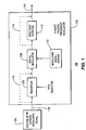
- Figure 1 is a functional block diagram of a digitized RF signal source coupled to a Nyquist folding frequency modulator, in accordance with the principles of the present invention.
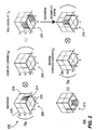
- Figure 2 depicts a z-Plane representation of the method for performing Nyquist folding frequency modulation in accordance with the principles of the present invention.
- Figure 1 depicts a functional block diagram of a Nyquist folding frequency modulator 102 coupled to an RF carrier modulated signal source 104.
- the source 104 provides a digitized RF carrier modulated signal having a defined bandwidth and a center frequency at carrier frequency f o .
- the RF carrier modulated signal is coupled to port 118 of the Nyquist folding frequency modulator 102.
- the Nyquist folding frequency modulator 102 comprises a resampler 106, a digital modulator 108, a spectrum inverter 110, and a modulating signal source 112.
- the resampler 106 changes the sampling rate of the RF carrier modulated signal.
- the sample rate at the output of resampler 106 is equal to twice the sum of the desired RF center frequency (frequency 3) and the present RF center frequency (frequency 1).
- the resampling process does not alter the carrier frequency of the RF carrier modulated signal but rather the density of samples representing the RF Signal. If the sampling rate at the input to resampler 106 equals the sample rate required at the output of the resampler 106, the resampler is not needed and would be bypassed as represented by path 114. Additionally, if the RF carrier modulated signal is an analog signal, then the resampler can be an analog-to-digital converter that samples the RF carrier modulated signal at the required sampling rate.
- the sampled RF carrier modulated signal (whether resampled or not) is coupled to a digital modulator 108.
- the modulating signal source 112 provides a repeating digital sequence of ⁇ 1,-1,1,-1,... ⁇ that is provided at a sample rate (f s ) equal to the resampler output sample rate.
- the center frequency of the output signal from the digital modulator 108 depends upon the relationship of the sample rate (f s ) and the carrier frequency (f 0 ) of the RF carrier modulated signal. If the sample rate (f s ) is exactly four times the carrier frequency (f 0 ), then the center frequency of the output signal is the same as the carrier frequency (f 0 ).
- the output of the digital modulator 108 is then the spectrum of the RF carrier modulated signal at a carrier frequency of f 0 . However, the digital modulator 108 using this particular modulating signal causes the spectrum of the RF carrier modulated signal to be inverted.
- the center frequency of the output signal is shifted to a carrier frequency (f 1 ) equal to one-half the sample rate minus the original RF carrier frequency i.e., (f s /2-f 0 ).
- the output of the digital modulator 108 is then the spectrum of the RF carrier modulated signal at a carrier frequency of f 1 with an inverted spectrum for the RF carrier modulated signal.
- a spectrum inverter 110 is applied to invert the RF signal spectrum and leave the carrier at f 0 or f 1 .
- the output at port 120 is the source RF carrier modulated signal at a carrier of frequency f 0 or f 1 .
- the spectrum inversion may be accomplished by performing an even number of Nyquist folding frequency modulations in the up-modulation chain. As such, the resampling and digital modulation would be repeated within the spectrum inverter 110 to achieve a non-inverted RF carrier modulated signal output.
- Another technique for performing spectrum inversion could be applied prior to remodulation (i.e., when the baseband signal was first modulated onto a carrier ). Such techniques include inverting the sign of the "imaginary" component of the complex baseband signal or changing the sign of the frequency of the first modulation complex carrier (invert the sine component).
- An additional spectral inversion can also be applied in the analog RF processing which often resides prior to or after the Nyquist folding frequency modulator 102.
- the spectrum inversion may just be ignored as irrelevant.
- the spectrum inversion has no effect.
- the spectrum inverter 110 may be excluded from the Nyquist folding frequency modulator 102 as represented by dashed line 116.
- FIG. 2 depicts a z-Plane representation 200 of the method of performing Nyquist folding frequency modulation of the present invention.
- the RF carrier modulated signal is represented by the real part of the baseband signal 206 convolved with the complex carrier 208. This process is represented at reference number 202.
- the folding frequency modulation technique takes advantage of the fact that sampled data in the frequency domain is linearly cyclic. The highest frequency of the cyclic frequencies is termed the Nyquist Folding Frequency (half of the sampling rate (f s ).
- each point along the circumference of a unit circle corresponds to a different complex carrier, e (j ⁇ o n) , ⁇ [- ⁇ , ⁇ ], where ⁇ is a normalized radian frequency corresponding to the Nyquist Folding Frequency.
- ⁇ is a normalized radian frequency corresponding to the Nyquist Folding Frequency.
- the modulated signal is generally created as the real part of a time domain product of a complex base band signal 206 having a zero frequency carrier 208 having a complex carrier frequency of f 0 .
- the real portion of this signal is represented by graph 204.
- the signal 204 is resampled to a predefined sample rate and modulated by the repeating sequence ⁇ 1,-1,1,-1,... ⁇ at a sample rate (f s ) that yields an RF carrier modulated signal with a carrier at frequency f 1 .
- a side effect of the second modulation is that the sine component is inverted by this operation. This inversion can be reversed as described above.
- the output frequency of the digital RF is at the difference frequency (f 1 ) of the carrier (f 0 ) and one-half the sampling rate (f s ) as depicted in the graph 212.
Landscapes
- Engineering & Computer Science (AREA)
- Power Engineering (AREA)
- Digital Transmission Methods That Use Modulated Carrier Waves (AREA)
- Amplitude Modulation (AREA)
- Signal Processing For Digital Recording And Reproducing (AREA)
Abstract
Description
One of these carriers is unique in that it is real, εj ·π· n = Cos(π·n). There is no corresponding complex carrier in the continuous time unbounded frequency domain. When this special carrier is combined with sample rate conversion (time scale change), re-modulation can be performed without the attendant extra processing of the various methods of the prior art. Each 3D graph diagrams the z-Plane frequency domain of a signal. Note that while multiple iterations could be used to advantage in some applications, only one stage of re-modulation is diagrammed in Figure 2. The three
Claims (13)
- A method for re-modulating a signal characterized by:modulating a RF carrier modulated signal having a center frequency of a first frequency and time sampled at a second frequency with a repeating sample sequence of {1,-1,1,-1...}, at the sample rate of the second frequency to produce a remodulated RF carrier modulated signal whose center frequency is a third frequency.
- The method of claim 1 characterized in that said second frequency is equal to four times the first frequency resulting in the third frequency being equal to the first frequency.
- The method of claim 1 further characterized by:resampling the digitized RF carrier modulated signal prior to said modulating step.
- The method of claim 1 further characterized by:inverting a spectrum of the remodulated RF carrier modulated signal.
- A method for re-modulating a RF carrier modulated signal comprising:sampling an analog RF carrier modulated signal to form a digitized RF carrier modulated signal having a carrier frequency of a first frequency;modulating the digitized RF carrier modulated signal with a repeating sequence of 1-1,1-1..., having a sample rate of a second frequency to produce a remodulated RF carrier modulated signal; andinverting a spectrum of the remodulated RF carrier modulated signal.
- The method of claim 5 characterized in that said remodulated RF carrier modulated signal has a carrier frequency equal to the first frequency minus one-half of the second frequency.
- The method of claim 5 wherein said sampling is performed by an analog-to-digital converter.
- A method for re-modulating a RF carrier modulated signal characterized by:resampling a digital RF carrier modulated signal to form a digitized RF carrier modulated signal having a carrier frequency of a first frequency;modulating the digitized RF carrier modulated signal with a repeating sequence of 1-1,1-1..., having a sample rate of a second frequency to produce a remodulated RF carrier modulated signal; andinverting a spectrum of the remodulated RF carrier modulated signal.
- The method of claim 5 characterized in that said remodulated RF carrier modulated signal has a carrier frequency equal to the first frequency minus one-half of the second frequency.
- Apparatus for re-modulating a signal characterized by:a modulating signal source (112) providing a repeating digital sequence of 1,-1,1,-1..., having a sample rate of a second frequency;a digital modulator (108) for sampling a digitized RF carrier modulated signal having a center frequency of a first frequency using the digital sequence to produce a remodulated RF carrier modulated signal whose carrier is a third frequency.
- The apparatus of claim 10 characterized in that said second frequency is equal to four times the first frequency resulting in the third frequency being equal to the first frequency.
- The apparatus of claim 10 further characterized by:a resampler (106) for resampling the digitized RF carrier modulated signal prior to said digital modulator.
- The apparatus of claim 10 further characterized by:a spectrum inverter (110) for inverting a spectrum of the remodulated RF carrier modulated signal.
Applications Claiming Priority (4)
| Application Number | Priority Date | Filing Date | Title |
|---|---|---|---|
| US32317401P | 2001-09-18 | 2001-09-18 | |
| US323174P | 2001-09-18 | ||
| US61102P | 2002-02-01 | ||
| US10/061,102 US7072418B2 (en) | 2001-09-18 | 2002-02-01 | Method and apparatus for performing Nyquist folding frequency modulation |
Publications (2)
| Publication Number | Publication Date |
|---|---|
| EP1294089A2 true EP1294089A2 (en) | 2003-03-19 |
| EP1294089A3 EP1294089A3 (en) | 2005-02-09 |
Family
ID=26740727
Family Applications (1)
| Application Number | Title | Priority Date | Filing Date |
|---|---|---|---|
| EP02019639A Withdrawn EP1294089A3 (en) | 2001-09-18 | 2002-09-03 | Remodulation of an RF carrier modulated signal |
Country Status (8)
| Country | Link |
|---|---|
| US (1) | US7072418B2 (en) |
| EP (1) | EP1294089A3 (en) |
| JP (1) | JP4099021B2 (en) |
| KR (1) | KR100947520B1 (en) |
| CN (1) | CN1409525A (en) |
| BR (1) | BR0203662A (en) |
| MX (1) | MXPA02009138A (en) |
| MY (1) | MY134256A (en) |
Families Citing this family (3)
| Publication number | Priority date | Publication date | Assignee | Title |
|---|---|---|---|---|
| US7953174B2 (en) * | 2002-03-20 | 2011-05-31 | The Regents Of The University Of California | Radio transmission frequency digital signal generation |
| ES2221570B2 (en) * | 2003-05-30 | 2005-10-01 | Diseño De Sistemas En Silicio, S.A. | REMEDY PROCEDURE IN TRANSMISSION AND RECEPTION OF A DIGITAL SIGNAL WITH TRANSFER IN DIGITAL BAND. |
| KR102553660B1 (en) * | 2019-03-11 | 2023-07-07 | 최만림 | Apparatus, method and computer-readable recording medium for measuring the size of an electrocardiogram signal using the Hilbert transform |
Family Cites Families (17)
| Publication number | Priority date | Publication date | Assignee | Title |
|---|---|---|---|---|
| US4682106A (en) * | 1985-03-21 | 1987-07-21 | General Electric Company | Methods of, and apparatus for, proton decoupling in nuclear magnetic resonance spectroscopy |
| US4855894A (en) | 1987-05-25 | 1989-08-08 | Kabushiki Kaisha Kenwood | Frequency converting apparatus |
| US6104863A (en) | 1990-08-17 | 2000-08-15 | Samsung Electronics Co., Ltd. | Video signal encoded with additional detail information |
| US5532820A (en) | 1990-08-17 | 1996-07-02 | Samsung Electronics Co., Ltd. | Digital modulators for use with sub-nyquist sampling of raster-scanned samples of image intensity |
| JPH04290337A (en) * | 1991-03-19 | 1992-10-14 | Sony Corp | Orthogonal modulator |
| US5490173A (en) | 1993-07-02 | 1996-02-06 | Ford Motor Company | Multi-stage digital RF translator |
| CA2178815C (en) | 1994-12-05 | 1999-10-05 | Shoichi Narahashi | Device and method for multiplexing signal |
| JP2967710B2 (en) | 1995-09-29 | 1999-10-25 | 日本電気株式会社 | Digital modulator |
| JP3517056B2 (en) | 1996-04-24 | 2004-04-05 | パイオニア株式会社 | Sampling timing phase error detector for VSB modulated signal |
| GB2319939B (en) | 1996-11-27 | 2001-06-27 | Sony Uk Ltd | Signal processors |
| US5937013A (en) * | 1997-01-03 | 1999-08-10 | The Hong Kong University Of Science & Technology | Subharmonic quadrature sampling receiver and design |
| JP3428846B2 (en) | 1997-01-07 | 2003-07-22 | 株式会社鷹山 | Time diffusion root Nyquist filter |
| IT1294284B1 (en) * | 1997-07-29 | 1999-03-24 | Italtel Spa | WIDE BAND RADIO TRANSMITTER FOR A SIGNAL CONSTITUTED BY A PLURALITY OF EQUIPPED DIGITALLY MODULATED CARRIERS |
| US6459743B1 (en) | 1998-08-07 | 2002-10-01 | Telefonaktiebolaget Lm Ericsson (Publ) | Digital reception with radio frequency sampling |
| US6366629B1 (en) * | 1998-11-03 | 2002-04-02 | Tektronix, Inc. | Method of estimating timing phase and rate offsets in digital data |
| US6215430B1 (en) * | 1999-04-24 | 2001-04-10 | Motorola, Inc. | Method and apparatus for processing a digital signal for analog transmission |
| US7110732B2 (en) * | 2001-04-09 | 2006-09-19 | Texas Instruments Incorporated | Subsampling RF receiver architecture |
-
2002
- 2002-02-01 US US10/061,102 patent/US7072418B2/en not_active Expired - Fee Related
- 2002-09-03 EP EP02019639A patent/EP1294089A3/en not_active Withdrawn
- 2002-09-03 KR KR1020020052697A patent/KR100947520B1/en not_active Expired - Fee Related
- 2002-09-11 BR BR0203662-2A patent/BR0203662A/en not_active IP Right Cessation
- 2002-09-13 JP JP2002268936A patent/JP4099021B2/en not_active Expired - Fee Related
- 2002-09-17 MY MYPI20023466A patent/MY134256A/en unknown
- 2002-09-18 MX MXPA02009138A patent/MXPA02009138A/en active IP Right Grant
- 2002-09-18 CN CN02142817A patent/CN1409525A/en active Pending
Also Published As
| Publication number | Publication date |
|---|---|
| MY134256A (en) | 2007-11-30 |
| KR100947520B1 (en) | 2010-03-12 |
| US20030053551A1 (en) | 2003-03-20 |
| CN1409525A (en) | 2003-04-09 |
| MXPA02009138A (en) | 2005-07-25 |
| BR0203662A (en) | 2003-06-03 |
| KR20030024572A (en) | 2003-03-26 |
| JP2003115885A (en) | 2003-04-18 |
| US7072418B2 (en) | 2006-07-04 |
| EP1294089A3 (en) | 2005-02-09 |
| JP4099021B2 (en) | 2008-06-11 |
Similar Documents
| Publication | Publication Date | Title |
|---|---|---|
| US6724832B1 (en) | Vestigial sideband generator particularly for digital television | |
| Shtendel et al. | Unlimited sampling of bandpass signals: Computational demodulation via undersampling | |
| CN100399774C (en) | Communication system and corresponding receiver | |
| KR20040047807A (en) | Demodulation of multiple-carrier phase-modulated signals | |
| JPH0823231A (en) | Fm modulation circuit | |
| US5438686A (en) | Amplitude-modulated broadcast transmitter for various types of modulation, in particular DSB, SSB and ISB | |
| US7072418B2 (en) | Method and apparatus for performing Nyquist folding frequency modulation | |
| JPH0235483B2 (en) | ||
| AU762856B2 (en) | Carrier tracking method | |
| KR20050037385A (en) | Digital modulation circuit and digital modulation method, digital demodulation circuit and digital demodulation method, generation circuit and generation method of carrier for demodulation, generation circuit and generation method of bit clock for demodulation | |
| US7206357B2 (en) | System and method for an improved quadrature upconverter for I/Q modulation using intermediate frequency carriers | |
| US6831578B2 (en) | Method and circuit arrangement for demodulation of a quadrature amplitude- or phase-modulated signal | |
| US6771710B1 (en) | Partial frequency offset digital upconversion | |
| JP2000270037A (en) | Quadrature modulator | |
| RU2012011C1 (en) | Method for compensation of frequency shift in signal having unknown initial phase | |
| RU2007877C1 (en) | Method of transmission and reception of reflex-modulated signals | |
| JPH06216650A (en) | Digital circuit for extracting phase signal and envelope signal of single-sideband signal | |
| EP2797225B1 (en) | Method of and apparatus for demodulating an amplitude modulated signal | |
| EP0406423A1 (en) | Method for transmission and reception of reflex-modulated signals | |
| JPH03209918A (en) | Integral interpolating device for pcm modulator/ demodulator | |
| JPS61293006A (en) | Two-dimensional vestigial side-band wave modulator | |
| JPH03171953A (en) | Linear modulator | |
| JPH08139770A (en) | Direct conversion receiver | |
| JPH05252213A (en) | Digital FM modulator | |
| JPH02309841A (en) | Modulator |
Legal Events
| Date | Code | Title | Description |
|---|---|---|---|
| PUAI | Public reference made under article 153(3) epc to a published international application that has entered the european phase |
Free format text: ORIGINAL CODE: 0009012 |
|
| AK | Designated contracting states |
Kind code of ref document: A2 Designated state(s): AT BE BG CH CY CZ DE DK EE ES FI FR GB GR IE IT LI LU MC NL PT SE SK TR Designated state(s): AT BE BG CH CY CZ DE DK EE ES FI FR GB GR IE IT LI LU MC NL PT SE SK TR |
|
| AX | Request for extension of the european patent |
Extension state: AL LT LV MK RO SI |
|
| PUAL | Search report despatched |
Free format text: ORIGINAL CODE: 0009013 |
|
| AK | Designated contracting states |
Kind code of ref document: A3 Designated state(s): AT BE BG CH CY CZ DE DK EE ES FI FR GB GR IE IT LI LU MC NL PT SE SK TR |
|
| AX | Request for extension of the european patent |
Extension state: AL LT LV MK RO SI |
|
| 17P | Request for examination filed |
Effective date: 20050707 |
|
| RAP1 | Party data changed (applicant data changed or rights of an application transferred) |
Owner name: THOMSON LICENSING |
|
| AKX | Designation fees paid |
Designated state(s): DE ES FR GB IT |
|
| RAP1 | Party data changed (applicant data changed or rights of an application transferred) |
Owner name: THOMSON LICENSING |
|
| STAA | Information on the status of an ep patent application or granted ep patent |
Free format text: STATUS: THE APPLICATION IS DEEMED TO BE WITHDRAWN |
|
| 18D | Application deemed to be withdrawn |
Effective date: 20120612 |