EP1294023A2 - Semiconductor integrated circuit modules, manufacturing methods and usage thereof - Google Patents
Semiconductor integrated circuit modules, manufacturing methods and usage thereof Download PDFInfo
- Publication number
- EP1294023A2 EP1294023A2 EP02003595A EP02003595A EP1294023A2 EP 1294023 A2 EP1294023 A2 EP 1294023A2 EP 02003595 A EP02003595 A EP 02003595A EP 02003595 A EP02003595 A EP 02003595A EP 1294023 A2 EP1294023 A2 EP 1294023A2
- Authority
- EP
- European Patent Office
- Prior art keywords
- power supply
- package
- semiconductor integrated
- integrated circuit
- supply module
- Prior art date
- Legal status (The legal status is an assumption and is not a legal conclusion. Google has not performed a legal analysis and makes no representation as to the accuracy of the status listed.)
- Granted
Links
Images



Classifications
-
- H—ELECTRICITY
- H05—ELECTRIC TECHNIQUES NOT OTHERWISE PROVIDED FOR
- H05K—PRINTED CIRCUITS; CASINGS OR CONSTRUCTIONAL DETAILS OF ELECTRIC APPARATUS; MANUFACTURE OF ASSEMBLAGES OF ELECTRICAL COMPONENTS
- H05K1/00—Printed circuits
- H05K1/18—Printed circuits structurally associated with non-printed electric components
- H05K1/181—Printed circuits structurally associated with non-printed electric components associated with surface mounted components
-
- H—ELECTRICITY
- H05—ELECTRIC TECHNIQUES NOT OTHERWISE PROVIDED FOR
- H05K—PRINTED CIRCUITS; CASINGS OR CONSTRUCTIONAL DETAILS OF ELECTRIC APPARATUS; MANUFACTURE OF ASSEMBLAGES OF ELECTRICAL COMPONENTS
- H05K1/00—Printed circuits
- H05K1/02—Details
- H05K1/14—Structural association of two or more printed circuits
- H05K1/141—One or more single auxiliary printed circuits mounted on a main printed circuit, e.g. modules, adapters
-
- H—ELECTRICITY
- H10—SEMICONDUCTOR DEVICES; ELECTRIC SOLID-STATE DEVICES NOT OTHERWISE PROVIDED FOR
- H10W—GENERIC PACKAGES, INTERCONNECTIONS, CONNECTORS OR OTHER CONSTRUCTIONAL DETAILS OF DEVICES COVERED BY CLASS H10
- H10W40/00—Arrangements for thermal protection or thermal control
- H10W40/20—Arrangements for cooling
- H10W40/22—Arrangements for cooling characterised by their shape, e.g. having conical or cylindrical projections
-
- H—ELECTRICITY
- H10—SEMICONDUCTOR DEVICES; ELECTRIC SOLID-STATE DEVICES NOT OTHERWISE PROVIDED FOR
- H10W—GENERIC PACKAGES, INTERCONNECTIONS, CONNECTORS OR OTHER CONSTRUCTIONAL DETAILS OF DEVICES COVERED BY CLASS H10
- H10W42/00—Arrangements for protection of devices
- H10W42/20—Arrangements for protection of devices protecting against electromagnetic or particle radiation, e.g. light, X-rays, gamma-rays or electrons
-
- H—ELECTRICITY
- H10—SEMICONDUCTOR DEVICES; ELECTRIC SOLID-STATE DEVICES NOT OTHERWISE PROVIDED FOR
- H10W—GENERIC PACKAGES, INTERCONNECTIONS, CONNECTORS OR OTHER CONSTRUCTIONAL DETAILS OF DEVICES COVERED BY CLASS H10
- H10W70/00—Package substrates; Interposers; Redistribution layers [RDL]
- H10W70/60—Insulating or insulated package substrates; Interposers; Redistribution layers
- H10W70/67—Insulating or insulated package substrates; Interposers; Redistribution layers characterised by their insulating layers or insulating parts
- H10W70/68—Shapes or dispositions thereof
-
- H—ELECTRICITY
- H10—SEMICONDUCTOR DEVICES; ELECTRIC SOLID-STATE DEVICES NOT OTHERWISE PROVIDED FOR
- H10W—GENERIC PACKAGES, INTERCONNECTIONS, CONNECTORS OR OTHER CONSTRUCTIONAL DETAILS OF DEVICES COVERED BY CLASS H10
- H10W74/00—Encapsulations, e.g. protective coatings
- H10W74/10—Encapsulations, e.g. protective coatings characterised by their shape or disposition
- H10W74/111—Encapsulations, e.g. protective coatings characterised by their shape or disposition the semiconductor body being completely enclosed
- H10W74/114—Encapsulations, e.g. protective coatings characterised by their shape or disposition the semiconductor body being completely enclosed by a substrate and the encapsulations
- H10W74/117—Encapsulations, e.g. protective coatings characterised by their shape or disposition the semiconductor body being completely enclosed by a substrate and the encapsulations the substrate having spherical bumps for external connection
-
- H—ELECTRICITY
- H10—SEMICONDUCTOR DEVICES; ELECTRIC SOLID-STATE DEVICES NOT OTHERWISE PROVIDED FOR
- H10W—GENERIC PACKAGES, INTERCONNECTIONS, CONNECTORS OR OTHER CONSTRUCTIONAL DETAILS OF DEVICES COVERED BY CLASS H10
- H10W76/00—Containers; Fillings or auxiliary members therefor; Seals
- H10W76/40—Fillings or auxiliary members in containers, e.g. centering rings
- H10W76/42—Fillings
- H10W76/47—Solid or gel fillings
-
- H—ELECTRICITY
- H10—SEMICONDUCTOR DEVICES; ELECTRIC SOLID-STATE DEVICES NOT OTHERWISE PROVIDED FOR
- H10W—GENERIC PACKAGES, INTERCONNECTIONS, CONNECTORS OR OTHER CONSTRUCTIONAL DETAILS OF DEVICES COVERED BY CLASS H10
- H10W90/00—Package configurations
-
- H—ELECTRICITY
- H05—ELECTRIC TECHNIQUES NOT OTHERWISE PROVIDED FOR
- H05K—PRINTED CIRCUITS; CASINGS OR CONSTRUCTIONAL DETAILS OF ELECTRIC APPARATUS; MANUFACTURE OF ASSEMBLAGES OF ELECTRICAL COMPONENTS
- H05K1/00—Printed circuits
- H05K1/02—Details
- H05K1/0213—Electrical arrangements not otherwise provided for
- H05K1/0254—High voltage adaptations; Electrical insulation details; Overvoltage or electrostatic discharge protection ; Arrangements for regulating voltages or for using plural voltages
- H05K1/0262—Arrangements for regulating voltages or for using plural voltages
-
- H—ELECTRICITY
- H05—ELECTRIC TECHNIQUES NOT OTHERWISE PROVIDED FOR
- H05K—PRINTED CIRCUITS; CASINGS OR CONSTRUCTIONAL DETAILS OF ELECTRIC APPARATUS; MANUFACTURE OF ASSEMBLAGES OF ELECTRICAL COMPONENTS
- H05K2201/00—Indexing scheme relating to printed circuits covered by H05K1/00
- H05K2201/10—Details of components or other objects attached to or integrated in a printed circuit board
- H05K2201/10431—Details of mounted components
- H05K2201/10507—Involving several components
- H05K2201/10515—Stacked components
-
- H—ELECTRICITY
- H05—ELECTRIC TECHNIQUES NOT OTHERWISE PROVIDED FOR
- H05K—PRINTED CIRCUITS; CASINGS OR CONSTRUCTIONAL DETAILS OF ELECTRIC APPARATUS; MANUFACTURE OF ASSEMBLAGES OF ELECTRICAL COMPONENTS
- H05K2201/00—Indexing scheme relating to printed circuits covered by H05K1/00
- H05K2201/10—Details of components or other objects attached to or integrated in a printed circuit board
- H05K2201/10431—Details of mounted components
- H05K2201/10507—Involving several components
- H05K2201/1053—Mounted components directly electrically connected to each other, i.e. not via the PCB
-
- H—ELECTRICITY
- H05—ELECTRIC TECHNIQUES NOT OTHERWISE PROVIDED FOR
- H05K—PRINTED CIRCUITS; CASINGS OR CONSTRUCTIONAL DETAILS OF ELECTRIC APPARATUS; MANUFACTURE OF ASSEMBLAGES OF ELECTRICAL COMPONENTS
- H05K2201/00—Indexing scheme relating to printed circuits covered by H05K1/00
- H05K2201/10—Details of components or other objects attached to or integrated in a printed circuit board
- H05K2201/10613—Details of electrical connections of non-printed components, e.g. special leads
- H05K2201/10621—Components characterised by their electrical contacts
- H05K2201/10689—Leaded Integrated Circuit [IC] package, e.g. dual-in-line [DIL]
-
- H—ELECTRICITY
- H05—ELECTRIC TECHNIQUES NOT OTHERWISE PROVIDED FOR
- H05K—PRINTED CIRCUITS; CASINGS OR CONSTRUCTIONAL DETAILS OF ELECTRIC APPARATUS; MANUFACTURE OF ASSEMBLAGES OF ELECTRICAL COMPONENTS
- H05K2201/00—Indexing scheme relating to printed circuits covered by H05K1/00
- H05K2201/10—Details of components or other objects attached to or integrated in a printed circuit board
- H05K2201/10613—Details of electrical connections of non-printed components, e.g. special leads
- H05K2201/10621—Components characterised by their electrical contacts
- H05K2201/10734—Ball grid array [BGA]; Bump grid array
-
- H—ELECTRICITY
- H10—SEMICONDUCTOR DEVICES; ELECTRIC SOLID-STATE DEVICES NOT OTHERWISE PROVIDED FOR
- H10W—GENERIC PACKAGES, INTERCONNECTIONS, CONNECTORS OR OTHER CONSTRUCTIONAL DETAILS OF DEVICES COVERED BY CLASS H10
- H10W40/00—Arrangements for thermal protection or thermal control
- H10W40/40—Arrangements for thermal protection or thermal control involving heat exchange by flowing fluids
- H10W40/43—Arrangements for thermal protection or thermal control involving heat exchange by flowing fluids by flowing gases, e.g. forced air cooling
-
- H—ELECTRICITY
- H10—SEMICONDUCTOR DEVICES; ELECTRIC SOLID-STATE DEVICES NOT OTHERWISE PROVIDED FOR
- H10W—GENERIC PACKAGES, INTERCONNECTIONS, CONNECTORS OR OTHER CONSTRUCTIONAL DETAILS OF DEVICES COVERED BY CLASS H10
- H10W70/00—Package substrates; Interposers; Redistribution layers [RDL]
- H10W70/40—Leadframes
-
- H—ELECTRICITY
- H10—SEMICONDUCTOR DEVICES; ELECTRIC SOLID-STATE DEVICES NOT OTHERWISE PROVIDED FOR
- H10W—GENERIC PACKAGES, INTERCONNECTIONS, CONNECTORS OR OTHER CONSTRUCTIONAL DETAILS OF DEVICES COVERED BY CLASS H10
- H10W70/00—Package substrates; Interposers; Redistribution layers [RDL]
- H10W70/60—Insulating or insulated package substrates; Interposers; Redistribution layers
-
- H—ELECTRICITY
- H10—SEMICONDUCTOR DEVICES; ELECTRIC SOLID-STATE DEVICES NOT OTHERWISE PROVIDED FOR
- H10W—GENERIC PACKAGES, INTERCONNECTIONS, CONNECTORS OR OTHER CONSTRUCTIONAL DETAILS OF DEVICES COVERED BY CLASS H10
- H10W70/00—Package substrates; Interposers; Redistribution layers [RDL]
- H10W70/60—Insulating or insulated package substrates; Interposers; Redistribution layers
- H10W70/67—Insulating or insulated package substrates; Interposers; Redistribution layers characterised by their insulating layers or insulating parts
- H10W70/68—Shapes or dispositions thereof
- H10W70/682—Shapes or dispositions thereof comprising holes having chips therein
-
- H—ELECTRICITY
- H10—SEMICONDUCTOR DEVICES; ELECTRIC SOLID-STATE DEVICES NOT OTHERWISE PROVIDED FOR
- H10W—GENERIC PACKAGES, INTERCONNECTIONS, CONNECTORS OR OTHER CONSTRUCTIONAL DETAILS OF DEVICES COVERED BY CLASS H10
- H10W70/00—Package substrates; Interposers; Redistribution layers [RDL]
- H10W70/60—Insulating or insulated package substrates; Interposers; Redistribution layers
- H10W70/67—Insulating or insulated package substrates; Interposers; Redistribution layers characterised by their insulating layers or insulating parts
- H10W70/68—Shapes or dispositions thereof
- H10W70/685—Shapes or dispositions thereof comprising multiple insulating layers
-
- H—ELECTRICITY
- H10—SEMICONDUCTOR DEVICES; ELECTRIC SOLID-STATE DEVICES NOT OTHERWISE PROVIDED FOR
- H10W—GENERIC PACKAGES, INTERCONNECTIONS, CONNECTORS OR OTHER CONSTRUCTIONAL DETAILS OF DEVICES COVERED BY CLASS H10
- H10W72/00—Interconnections or connectors in packages
- H10W72/071—Connecting or disconnecting
- H10W72/075—Connecting or disconnecting of bond wires
- H10W72/07551—Connecting or disconnecting of bond wires characterised by changes in properties of the bond wires during the connecting
- H10W72/07554—Connecting or disconnecting of bond wires characterised by changes in properties of the bond wires during the connecting changes in dispositions
-
- H—ELECTRICITY
- H10—SEMICONDUCTOR DEVICES; ELECTRIC SOLID-STATE DEVICES NOT OTHERWISE PROVIDED FOR
- H10W—GENERIC PACKAGES, INTERCONNECTIONS, CONNECTORS OR OTHER CONSTRUCTIONAL DETAILS OF DEVICES COVERED BY CLASS H10
- H10W72/00—Interconnections or connectors in packages
- H10W72/50—Bond wires
- H10W72/541—Dispositions of bond wires
- H10W72/547—Dispositions of multiple bond wires
-
- H—ELECTRICITY
- H10—SEMICONDUCTOR DEVICES; ELECTRIC SOLID-STATE DEVICES NOT OTHERWISE PROVIDED FOR
- H10W—GENERIC PACKAGES, INTERCONNECTIONS, CONNECTORS OR OTHER CONSTRUCTIONAL DETAILS OF DEVICES COVERED BY CLASS H10
- H10W74/00—Encapsulations, e.g. protective coatings
-
- H—ELECTRICITY
- H10—SEMICONDUCTOR DEVICES; ELECTRIC SOLID-STATE DEVICES NOT OTHERWISE PROVIDED FOR
- H10W—GENERIC PACKAGES, INTERCONNECTIONS, CONNECTORS OR OTHER CONSTRUCTIONAL DETAILS OF DEVICES COVERED BY CLASS H10
- H10W90/00—Package configurations
- H10W90/701—Package configurations characterised by the relative positions of pads or connectors relative to package parts
- H10W90/721—Package configurations characterised by the relative positions of pads or connectors relative to package parts of bump connectors
- H10W90/722—Package configurations characterised by the relative positions of pads or connectors relative to package parts of bump connectors between stacked chips
-
- H—ELECTRICITY
- H10—SEMICONDUCTOR DEVICES; ELECTRIC SOLID-STATE DEVICES NOT OTHERWISE PROVIDED FOR
- H10W—GENERIC PACKAGES, INTERCONNECTIONS, CONNECTORS OR OTHER CONSTRUCTIONAL DETAILS OF DEVICES COVERED BY CLASS H10
- H10W90/00—Package configurations
- H10W90/701—Package configurations characterised by the relative positions of pads or connectors relative to package parts
- H10W90/751—Package configurations characterised by the relative positions of pads or connectors relative to package parts of bond wires
- H10W90/754—Package configurations characterised by the relative positions of pads or connectors relative to package parts of bond wires between a chip and a stacked insulating package substrate, interposer or RDL
-
- H—ELECTRICITY
- H10—SEMICONDUCTOR DEVICES; ELECTRIC SOLID-STATE DEVICES NOT OTHERWISE PROVIDED FOR
- H10W—GENERIC PACKAGES, INTERCONNECTIONS, CONNECTORS OR OTHER CONSTRUCTIONAL DETAILS OF DEVICES COVERED BY CLASS H10
- H10W90/00—Package configurations
- H10W90/701—Package configurations characterised by the relative positions of pads or connectors relative to package parts
- H10W90/751—Package configurations characterised by the relative positions of pads or connectors relative to package parts of bond wires
- H10W90/756—Package configurations characterised by the relative positions of pads or connectors relative to package parts of bond wires between a chip and a stacked lead frame, conducting package substrate or heat sink
-
- Y—GENERAL TAGGING OF NEW TECHNOLOGICAL DEVELOPMENTS; GENERAL TAGGING OF CROSS-SECTIONAL TECHNOLOGIES SPANNING OVER SEVERAL SECTIONS OF THE IPC; TECHNICAL SUBJECTS COVERED BY FORMER USPC CROSS-REFERENCE ART COLLECTIONS [XRACs] AND DIGESTS
- Y02—TECHNOLOGIES OR APPLICATIONS FOR MITIGATION OR ADAPTATION AGAINST CLIMATE CHANGE
- Y02P—CLIMATE CHANGE MITIGATION TECHNOLOGIES IN THE PRODUCTION OR PROCESSING OF GOODS
- Y02P70/00—Climate change mitigation technologies in the production process for final industrial or consumer products
- Y02P70/50—Manufacturing or production processes characterised by the final manufactured product
Definitions
- the present invention relates to a package enclosing a semiconductor integrated circuit or a semiconductor chip and to a power supply module that supplies power to the package, and more particularly to a semiconductor integrated circuit module comprising a power supply module provided in the direction perpendicular to the surface of the package and in the vicinity thereof.
- a power supply module is mounted on a package enclosing or sealing a semiconductor integrated circuit (IC, LSI), in the direction perpendicular to the surface of the package.
- the pin arrangement of the power supply module is standardised.
- the package and the power supply module disposed in the vicinity thereof are handled as a semiconductor integrated circuit module.
- a signal such as an input/output voltage of the power supply module is input in a voltage variation detection circuit unit provided inside a chip such as LSI.
- the power supply distance between the power supply module and a chip, such as LSI, serving as a load therefor can be shortened. Therefore, the radiation of power source noise can be reduced. Moreover, since shortening of the power supply distance decreases the resistance and inductance of the power supply line, the efficiency of the power supply unit of the power supply module is increased, the variations of the power supply voltage are reduced, and a high-speed response is made possible.
- power supply modules required for each package can be mounted on individual packages. Therefore, they can be handled as semiconductor integrated circuit modules. As a result, the number of power source types (voltage types) required for the substrate can be decreased and the mounting efficiency of the substrate is improved. Furthermore, even with the power source of one type, since the power supply module can be mounted on the upper surface of an LSI package, the mounting efficiency of the substrate is increased.
- FIG. 12 A structure in which a power supply module 11 is mounted in the direction perpendicular to the surface of LSI package 13 and they are disposed on a substrate 16 is shown on the right side of FIG. 12; this structure is the preferred embodiment of the present invention.
- the LSI package 13 contains an LSI chip 19 , and the power supply path from the module 11 to the chip 19 and back to the module 11 is shortened, as shown in the figure. Furthermore, in this configuration, the module 11 is provided close to the shield surface of package 13 and the unnecessary radiation of electromagnetic noise from the module 11 is effectively suppressed.
- FIG. 12 A conventional structure is shown on the left side of FIG. 12.
- the power supply module 11 and LSI package 13 are independently mounted on the substrate 16 .
- the power supply module 11 is disposed close to the LSI package 13 , a distance of power supply via the inner layers 321, 322 of substrate 16 is required.
- the power supply path from the power supply module 11 to the LSI chip 19 and back to the power supply module 11 is longer than that in the structure on the right side of FIG. 12.
- this power supply path is equivalent to an antenna, and if the module 11 or chip 19 serve as an electromagnetic noise source, it becomes a path where unnecessary electromagnetic waves are emitted.
- electromagnetic waves of preset frequency are also received and an adverse effect is produced on the operation of the LSI chip.
- the power supply distance can be greatly shortened by comparison with the conventional configuration and the reduction of power source noise, a high efficiency and high-speed response of the power supply unit, and the reduction of the emitted electromagnetic field can be realised.
- LSI chips operating at GHz frequencies have been also used in recent years and there is a possibility that the power supply paths with a length of several centimetres will be equivalent to a GHz-order antenna.
- the GHz-order electromagnetic waves generated by the LSI chips produce no adverse effect on the operation of power supply modules. This can be explained by the following reasons: ( 1 ) the power supply module itself cannot respond to the GHz-order electromagnetic waves, and ( 2 ) the circuit of the power supply module itself is shielded by the common mode and is hardly affected by the electromagnetic waves coming from the outside.
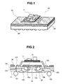
- FIGs. 1 and 2 illustrate the first embodiment of LSI module 23 employing the present invention.
- FIG. 2 is a cross-sectional view of the module shown in FIG. 1.
- a hole for installing a power supply module 11 is provided in a heat spreader 28 , and the configuration of leads of module 11 are such that they can be connected to electrodes 12 (not shown in the figure) located on the upper surface of LSI package 29 .
- the LSI package 29 has a substrate configuration on which the heat spreader 28 has been installed from the initial stage of the manufacture thereof thereby allowing for opening of the above-mentioned hole.
- the heat spreader 28 or a below-described heat sink 17 operates as a platy heat sink which emits the heat from the package or LSI chip.
- a through hole 301 (FIG. 2) connects a solder ball 181 and an electrode 121 .
- the input power is thus supplied to the power supply module 11 and the voltage Vmo regulated by the power supply module 11 is supplied to the LSI chip 19 via an electrode 122, a through hole 302, and a bonding wire 156.
- the power supply distance to the LSI chip 19 is shortened by comparison with that of the conventional technology and the reduction of power source noise, a high efficiency and high-speed response of the power supply unit, and the reduction of the emitted electromagnetic field can be realised.
- the chip 19 is secured to the heat spreader 28 with a silver paste 31 (FIG. 2), and after the prescribed electric connection to the LSI package 13 with bonding wires 153 ⁇ 156 has been conducted, the chip is sealed and enclosed in the package 13 with a chip sealing resin 22 .
- the heat spreader 28 is located between the LSI chip 19 and the power supply module 11 and it also plays a role of an electromagnetic shield. Therefore, the chip 19 is hardly affected by the noise produced by the power supply module 11 .
- FIGs. 3 and 4 illustrate the second embodiment of LSI module 23 in accordance with the present invention.
- FIG. 4 is a cross-sectional view of the module shown in FIG. 3. An opening is provided in the centre of power supply module 11 , and a heat sink 17 is installed on the LSI chip 19 , which is a load of power supply module 11 , via this opening (FIG. 4). The chip 19 is secured to the LSI package 13 with a chip sealing resin 23 .
- FIG. 5 shows the external appearance of LSI module 23 relating to a case when heat generation by the LSI chip 19 does nor require the heat sink 17 .
- the LSI module configuration of the first or third embodiment can more effectively suppress the unnecessary radiation of electromagnetic noise.
- FIGs. 6 and 7 illustrate the third embodiment of LSI module 23 employing the present invention.
- the power supply module 11 is mounted, while conducting electric connection via the electrodes 12 located on the upper surface of LSI package 13.
- Bonding wires 151 (FIG. 7) connect LSI lead pins 14 and electrodes 12. Power which serves as an input to the power supply module 11 is thus supplied and the output power regulated by the power supply module 11 is supplied to the LSI chip 19 via the bonding wires 152 connecting the electrodes 12 and LSI chip 19. As a result, the power supply distance to the LSI chip 19 becomes shorter than that in the conventional configurations and the reduction of power source noise, a high efficiency and high-speed response of the power supply unit, and the reduction of the emission electromagnetic field can be realised.
- the power supply module 11 having a standardised pin arrangement, which has to be connected thereto, can be installed on LSI package 13 or IC of other types and cost can be reduced by using common components.
- the production cost of module 23 can be reduced because only the power source module 11 can be replaced even if the power source module 11 becomes defective during or after the manufacture of LSI module 23 .
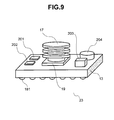
- FIG. 9 shows the fourth embodiment of LSI module 23 employing the present invention.
- the structural elements 201 ⁇ 204 of the power supply module were disposed on the LSI package 13. With this configuration, as with the configuration of the first embodiment, heat emission by the LSI chip 19 is not prevented. However, under conditions at which the present invention can be employed, the voltage Vp of the power source which is required for the LSI package 13 is the output voltage Vmo of power supply module 11 and is usually lower than the input voltage Vmi of power supply module 11.
- the package 13 has a structure capable of withstanding the voltage Vmi that has simply passed through the LSI package 13, (2) the input voltage Vmi is applied only to structural elements 201 ⁇ 204 of the power supply module of LSI package 13 and is not applied to other electronic elements of package 13 , and ( 3 ) the package 13 has a configuration such that only the output voltage Vmo of power supply module 11 is applied to other electronic elements of LSI package 13.
- the input voltage of LSI chip 19 has been decreased from 5 V to 3.3 V and 2.5 V, the technology employed to manufacture such LSI chip 19 is usually different from that used for the manufacture of power supply module 11 , and the LSI chip 19 does withstand the voltage Vmi applied to the power supply module 11 . For this reason, the chip 19 and module structural elements 201 ⁇ 204 have to be insulated by the wiring structure of LSI package 13.
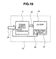
- FIG. 10 illustrates the fifth embodiment of LSI module 23 employing the present invention.
- the allowed range of power supply variations in the power supply line to LSI chip 19 is typically within 5 ⁇ 10% of the standard value.
- the power supply module 11 was not mounted on the LSI module. Therefore, the allowed range of power supply variations relating to the LSI module is equal to the allowed range of power supply variations relating to the LSI chip 19 .
- the power supply to the LSI module 23 is conducted to the LSI chip 19 via the power supply module 11 . Therefore, the allowed range of power supply variations relating to the LSI chip 19 can become the allowed range of power supply variations relating to the power supply module 11.
- the allowed range of power supply variations relating to the power supply module 11 typically may be within 10 ⁇ 20% of the standard value, the allowed range of power supply variations relating to the LSI chip 19 is expanded and the operation range of LSI module 23 is raised. Furthermore, a voltage variation detection circuit unit 27 provided inside the LSI chip 19 for detecting the power supply variations monitors not only the power supply line 25 relating to the LSI chip 19, but also the power supply line 24 relating to the LSI module. In other words, providing a line 26 for detecting voltage variation allows for rapid detection of abnormal voltage applied to the chip 19 .
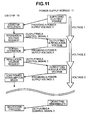
- FIG. 11 is a flow chart used to explain a method for bi-directional control between the LSI chip 19 and power supply module 11 in the LSI module 23 shown in FIG. 10.
- a power supply voltage 1 is supplied from the power supply module 11 , the start-up sequence of LSI chip 19 is initiated. Since the LSI chip 19 is required to operate at a high speed, when a voltage is required which is higher than the usual voltage, a control signal 1 is output from the LSI chip 19 to the power supply module 11 .
- the power supply module 11 receives the control signal 1 and outputs the requested power supply voltage 2 . Conversely, when the LSI chip 19 may operate at a voltage lower than the usual voltage in a low power consumption mode, the LSI chip 19 outputs a control signal 2 to the power supply module 11 . The power supply module 11 receives the control signal 2 and outputs the requested power supply voltage 3 .
- a control signal 3 is output from the power supply module 11 to the LSI chip 19 .
- the LSI chip 19 receives the control signal 3 and conducts a shutdown process.
- An LSI package as shown in the first embodiment (FIG. 1) has a heat spreader 28 on the surface and a hole for conducting electric connections is provided in the prescribed place.
- connection pattern or pin arrangement is made common and standard.
- a heat sink 17 may be installed, as shown in the second embodiment (FIG. 3). If heat generation by the LSI package is small, the heat sink or heat spreader may not be provided, as in the third embodiment (see FIG. 6).
- the wiring of power supply module and the wiring of LSI chip in the package 13 are completely insulated. Furthermore, a voltage variation detection circuit unit 27 is provided inside the LSI chip.
- the power supply module may be connected to the LSI package 29 , as in the first embodiment, and the connection may be made with solder balls 182 , as in the second embodiment.
- An opening for installing a heat sink 17 on the package is appropriately provided according to the amount of heat generated by the package.
- the wiring for the power supply module in the package 13 has to be insulated from the wiring for the LSI chip, except for the required power supply input and output.
- the LSI package and power supply module are stacked and mounted on a substrate so as to cause no drop in the mounting efficiency of the substrate onto which they are mounted.
- the power supply module is stacked on the perpendicular upper surface of LSI package, but the LSI package may be mounted on the power supply module. In this case, it is necessary to insulate the wiring of power supply module and the wiring of LSI chip and to provide a bypass line so as to form an electric connection to the substrate via the power supply module.
- Electromagnetic noise can be decreased, the power supply unit can operate with a high efficiency and high-speed response, and the unnecessary radiation of electromagnetic waves can be reduced.
- the emission of power source noise can be reduced because the power supply distance between the power supply module and a chip such as LSI chip serving as a load therefor can be shortened.
- Shortening the power supply distance decreases the power line resistance and inductance. Therefore, the efficiency of power supply unit of power supply module is increased, variations of power supply voltage are decreased, and a high-speed response is made possible.
- the power supply modules required for each package can be mounted on each package. Therefore, handling them as semiconductor integrated circuit modules makes it possible to reduce the number of power source types (voltage types) which are required to be on the substrate and the mounting efficiency of the substrate relating to mounting of electronic circuits other than power supply modules is increased.
- the power supply module can be mounted on the upper surface of LSI package, the mounting efficiency of the substrate is increased.
- the substrate surface and the internal power source plane can be a single surface and the substrate can be manufactured at a low cost.
- power supply module makes it possible to standardise the power supply modules and LSI packages. Therefore, power supply modules should not be designed for each LSI package, the number of design operations is decreased, and the production cost can be reduced.
Landscapes
- Engineering & Computer Science (AREA)
- Microelectronics & Electronic Packaging (AREA)
- Semiconductor Integrated Circuits (AREA)
- Shielding Devices Or Components To Electric Or Magnetic Fields (AREA)
- Cooling Or The Like Of Semiconductors Or Solid State Devices (AREA)
Abstract
Description
As a result, the power supply distance to the
Claims (16)
- A semiconductor integrated circuit module (23), comprising:a package (13) sealing a semiconductor integrated circuit (19); anda power supply module (11) mounted on said package and supplying power to said package.
- The circuit of claim 1, wherein
said power supply module comprises
a power supply chip unit or a power supply chip unit and peripheral components (201 - 204) thereof and
a plurality of electrodes (12, 121 - 122);
said package is provided with electrodes on the surface thereof; and
said power supply module is mounted on said package and power is supplied from said power supply module to said package by electrically connecting said electrodes to the electrodes of said power supply module. - A semiconductor integrated circuit module (23), comprising a package (13) sealing a semiconductor integrated circuit (19), and having structural components (201 - 204) of a power supply module (11) that supplies power to said package.
- The circuit of claim 2, further comprising:an interface between said semiconductor integrated circuit sealed by said package and said power supply module; andbi-directional control function (FIG. 11) between said semiconductor integrated circuit and said power supply module.
- The circuit of claim 4, wherein said power supply module is removable from said package.
- The circuit of claim 2, wherein said semiconductor integrated circuit module has a structure (FIGs. 3, 5 and 9) that enables itself to install a heat sink (17) after said power supply module was mounted.
- The circuit of claim 6, wherein said power supply module has an opening (FIGs. 3 and 5) and said heat sink can be installed via said opening.
- The circuit of claim 2, wherein the output voltage of said power supply module is lower than the input voltage of said package.
- A method for manufacturing a semiconductor integrated circuit module (23 in FIG. 3), comprising:conducting the following two operations in no specific order:(1) securing a semiconductor integrated circuit (19) to a package (13) and sealing therein; and(2) installing a platy heat sink (17) on the package; andmounting a power supply module (11) for power supply to said package from the direction substantially perpendicular to the surface of said package via said platy heat sink.
- A method for manufacturing a semiconductor integrated circuit module (23 in FIGs. 1, 3 and 5), comprising:securing a semiconductor integrated circuit (19) to a package (13) and sealing therein; andmounting a power supply module (11) for power supply to said package from the direction substantially perpendicular to the surface of said package.
- The method of claim 10 for a semiconductor integrated circuit module (23 in FIG. 3), further comprising providing a platy heat sink (17) on said package through an opening provided in said power supply module.
- A method for manufacturing a semiconductor integrated circuit module (23), wherein the following three operations are conducted in no specific order:(1) providing wirings of at least two systems on a package (13);(2) securing a semiconductor integrated circuit (19) to one of the wirings of the package and sealing therein; and(3) connecting the structural elements (201 - 204) of a power supply module (11) for power supply to the package, to another of the wirings of the package.
- The method of claim 12, further comprising providing said package with a platy heat sink.
- The method of claim 9, 10, or 12, comprising providing inside said semiconductor integrated circuit (19) a voltage variation detection circuit unit (27) for monitoring both said power supply to said semiconductor integrated circuit module and said power supply to said semiconductor integrated circuit, prior to securing said semiconductor integrated circuit to said package.
- A method of using a semiconductor integrated circuit module (23) having a package (13) sealing a semiconductor integrated circuit (19), and a power supply module (11) mounted on said package and supplying power to said package, the method comprising:supplying a first voltage from said power supply module to said semiconductor integrated circuit;said semiconductor integrated circuit initiating a start-up sequence;said semiconductor integrated circuit outputting a first control signal to said power supply module; andsaid power supply module outputting a second voltage to said semiconductor integrated circuit in response to said first control signal.
- A method of using a semiconductor integrated circuit module (23) having a package (13) sealing a semiconductor integrated circuit (19), and a power supply module (11) mounted on said package and supplying power to said package, the method comprising:supplying a first voltage from said power supply module to said semiconductor integrated circuit;said semiconductor integrated circuit initiating a start-up sequence;said power supply module outputting a third control signal to said semiconductor integrated circuit; andsaid semiconductor integrated circuit conducting a shutdown process upon reception of said third control signal.
Priority Applications (2)
| Application Number | Priority Date | Filing Date | Title |
|---|---|---|---|
| EP05028092A EP1650804A3 (en) | 2001-09-12 | 2002-02-15 | Semiconductor integrated circuit modules, manufacturing methods and usage thereof |
| EP05028093A EP1650805A3 (en) | 2001-09-12 | 2002-02-15 | Semiconductor integrated circuit modules, manufacturing methods and usage thereof |
Applications Claiming Priority (2)
| Application Number | Priority Date | Filing Date | Title |
|---|---|---|---|
| JP2001275887 | 2001-09-12 | ||
| JP2001275887A JP3944369B2 (en) | 2001-09-12 | 2001-09-12 | Semiconductor integrated circuit module and method of using the same |
Related Child Applications (2)
| Application Number | Title | Priority Date | Filing Date |
|---|---|---|---|
| EP05028092A Division EP1650804A3 (en) | 2001-09-12 | 2002-02-15 | Semiconductor integrated circuit modules, manufacturing methods and usage thereof |
| EP05028093A Division EP1650805A3 (en) | 2001-09-12 | 2002-02-15 | Semiconductor integrated circuit modules, manufacturing methods and usage thereof |
Publications (3)
| Publication Number | Publication Date |
|---|---|
| EP1294023A2 true EP1294023A2 (en) | 2003-03-19 |
| EP1294023A3 EP1294023A3 (en) | 2004-12-29 |
| EP1294023B1 EP1294023B1 (en) | 2008-06-18 |
Family
ID=19100674
Family Applications (3)
| Application Number | Title | Priority Date | Filing Date |
|---|---|---|---|
| EP05028092A Withdrawn EP1650804A3 (en) | 2001-09-12 | 2002-02-15 | Semiconductor integrated circuit modules, manufacturing methods and usage thereof |
| EP02003595A Expired - Lifetime EP1294023B1 (en) | 2001-09-12 | 2002-02-15 | Semiconductor integrated circuit modules, manufacturing methods and usage thereof |
| EP05028093A Withdrawn EP1650805A3 (en) | 2001-09-12 | 2002-02-15 | Semiconductor integrated circuit modules, manufacturing methods and usage thereof |
Family Applications Before (1)
| Application Number | Title | Priority Date | Filing Date |
|---|---|---|---|
| EP05028092A Withdrawn EP1650804A3 (en) | 2001-09-12 | 2002-02-15 | Semiconductor integrated circuit modules, manufacturing methods and usage thereof |
Family Applications After (1)
| Application Number | Title | Priority Date | Filing Date |
|---|---|---|---|
| EP05028093A Withdrawn EP1650805A3 (en) | 2001-09-12 | 2002-02-15 | Semiconductor integrated circuit modules, manufacturing methods and usage thereof |
Country Status (4)
| Country | Link |
|---|---|
| US (1) | US6777795B2 (en) |
| EP (3) | EP1650804A3 (en) |
| JP (1) | JP3944369B2 (en) |
| DE (1) | DE60227139D1 (en) |
Cited By (1)
| Publication number | Priority date | Publication date | Assignee | Title |
|---|---|---|---|---|
| EP1744604A1 (en) * | 2005-07-12 | 2007-01-17 | Alcatel | Amplifier with feedback bridge |
Families Citing this family (11)
| Publication number | Priority date | Publication date | Assignee | Title |
|---|---|---|---|---|
| JP2004288834A (en) * | 2003-03-20 | 2004-10-14 | Fujitsu Ltd | Electronic component mounting method, mounting structure and package substrate |
| US7732904B2 (en) * | 2003-10-10 | 2010-06-08 | Interconnect Portfolio Llc | Multi-surface contact IC packaging structures and assemblies |
| US7652381B2 (en) | 2003-11-13 | 2010-01-26 | Interconnect Portfolio Llc | Interconnect system without through-holes |
| WO2005050708A2 (en) * | 2003-11-13 | 2005-06-02 | Silicon Pipe, Inc. | Stair step printed circuit board structures for high speed signal transmissions |
| US7250672B2 (en) * | 2003-11-13 | 2007-07-31 | International Rectifier Corporation | Dual semiconductor die package with reverse lead form |
| US7278855B2 (en) | 2004-02-09 | 2007-10-09 | Silicon Pipe, Inc | High speed, direct path, stair-step, electronic connectors with improved signal integrity characteristics and methods for their manufacture |
| TWI237882B (en) * | 2004-05-11 | 2005-08-11 | Via Tech Inc | Stacked multi-chip package |
| DE102006033175A1 (en) * | 2006-07-18 | 2008-01-24 | Robert Bosch Gmbh | electronics assembly |
| US8253420B2 (en) * | 2009-12-04 | 2012-08-28 | Volterra Semiconductor Corporation | Integrated electrical circuit and test to determine the integrity of a silicon die |
| JP2014179484A (en) * | 2013-03-15 | 2014-09-25 | Toshiba Corp | Semiconductor memory device |
| KR102041644B1 (en) * | 2014-01-08 | 2019-11-07 | 삼성전기주식회사 | Power module package and method of fabricating the same |
Family Cites Families (15)
| Publication number | Priority date | Publication date | Assignee | Title |
|---|---|---|---|---|
| US5444298A (en) * | 1993-02-04 | 1995-08-22 | Intel Corporation | Voltage converting integrated circuit package |
| US5444296A (en) * | 1993-11-22 | 1995-08-22 | Sun Microsystems, Inc. | Ball grid array packages for high speed applications |
| US5556811A (en) * | 1993-12-21 | 1996-09-17 | Intel Corporation | Method of optimizing operating parameters of an integrated circuit package having a voltage regulator mounted thereon |
| US5440520A (en) * | 1994-09-16 | 1995-08-08 | Intel Corporation | Integrated circuit device that selects its own supply voltage by controlling a power supply |
| JPH08279593A (en) | 1995-04-04 | 1996-10-22 | Nec Corp | Semiconductor device that enables high-density mounting |
| US5694297A (en) * | 1995-09-05 | 1997-12-02 | Astec International Limited | Integrated circuit mounting structure including a switching power supply |
| US5808377A (en) * | 1996-01-11 | 1998-09-15 | Intel Corporation | Power supply contention prevention circuit |
| JPH11177015A (en) | 1997-12-11 | 1999-07-02 | Canon Inc | Semiconductor package and intermediate board for mounting semiconductor package |
| US6159765A (en) * | 1998-03-06 | 2000-12-12 | Microchip Technology, Incorporated | Integrated circuit package having interchip bonding and method therefor |
| US6181008B1 (en) * | 1998-11-12 | 2001-01-30 | Sarnoff Corporation | Integrated circuit power supply |
| JP2000349228A (en) | 1999-06-09 | 2000-12-15 | Hitachi Ltd | Stacked semiconductor package |
| JP4012655B2 (en) | 1999-08-30 | 2007-11-21 | 京セラ株式会社 | Semiconductor device |
| US6184580B1 (en) * | 1999-09-10 | 2001-02-06 | Siliconware Precision Industries Co., Ltd. | Ball grid array package with conductive leads |
| US6394175B1 (en) * | 2000-01-13 | 2002-05-28 | Lucent Technologies Inc. | Top mounted cooling device using heat pipes |
| KR100370231B1 (en) * | 2000-06-13 | 2003-01-29 | 페어차일드코리아반도체 주식회사 | Power module package having a insulator type heat sink attached a backside of leadframe & manufacturing method thereof |
-
2001
- 2001-09-12 JP JP2001275887A patent/JP3944369B2/en not_active Expired - Fee Related
-
2002
- 2002-02-15 EP EP05028092A patent/EP1650804A3/en not_active Withdrawn
- 2002-02-15 DE DE60227139T patent/DE60227139D1/en not_active Expired - Lifetime
- 2002-02-15 EP EP02003595A patent/EP1294023B1/en not_active Expired - Lifetime
- 2002-02-15 EP EP05028093A patent/EP1650805A3/en not_active Withdrawn
- 2002-02-20 US US10/077,779 patent/US6777795B2/en not_active Expired - Lifetime
Cited By (2)
| Publication number | Priority date | Publication date | Assignee | Title |
|---|---|---|---|---|
| EP1744604A1 (en) * | 2005-07-12 | 2007-01-17 | Alcatel | Amplifier with feedback bridge |
| US7417498B2 (en) | 2005-07-12 | 2008-08-26 | Alcatel | Amplifier with feedback bridge |
Also Published As
| Publication number | Publication date |
|---|---|
| EP1650804A3 (en) | 2010-09-08 |
| EP1650804A2 (en) | 2006-04-26 |
| JP3944369B2 (en) | 2007-07-11 |
| EP1650805A2 (en) | 2006-04-26 |
| US6777795B2 (en) | 2004-08-17 |
| EP1650805A3 (en) | 2010-09-08 |
| JP2003086754A (en) | 2003-03-20 |
| US20030047800A1 (en) | 2003-03-13 |
| DE60227139D1 (en) | 2008-07-31 |
| EP1294023A3 (en) | 2004-12-29 |
| EP1294023B1 (en) | 2008-06-18 |
Similar Documents
| Publication | Publication Date | Title |
|---|---|---|
| US7538441B2 (en) | Chip with power and signal pads connected to power and signal lines on substrate | |
| US6346743B1 (en) | Embedded capacitor assembly in a package | |
| US7215016B2 (en) | Multi-chips stacked package | |
| CN1139116C (en) | Integrated circuit package and computer system with the package | |
| US5789816A (en) | Multiple-chip integrated circuit package including a dummy chip | |
| US20100128451A1 (en) | Multilayered printed circuit board | |
| US5606199A (en) | Resin-molded type semiconductor device with tape carrier connection between chip electrodes and inner leads of lead frame | |
| JPH09148476A (en) | BGA type semiconductor device, components therefor and electronic device | |
| US6777795B2 (en) | Semiconductor integrated circuit modules, manufacturing methods and usage thereof | |
| JP7362380B2 (en) | Wiring boards and semiconductor devices | |
| US20220068734A1 (en) | Semiconductor device | |
| JPH09223861A (en) | Semiconductor integrated circuit and printed wiring board | |
| US8362614B2 (en) | Fine pitch grid array type semiconductor device | |
| CN103313507B (en) | Printed Circuit Board and System-on-Chip | |
| US20080136011A1 (en) | Semiconductor device | |
| US20050073050A1 (en) | BGA package and printed circuit board for supporting the package | |
| CN112768425B (en) | Multi-chip module | |
| WO1999013509A1 (en) | Semiconductor device | |
| US20120025898A1 (en) | Circuit Device | |
| US6281580B1 (en) | LSI package and inner lead wiring method for same | |
| JP2003007914A (en) | Semiconductor device | |
| CN100565861C (en) | Semiconductor device and manufacturing method thereof | |
| US7187065B2 (en) | Semiconductor device and semiconductor device unit | |
| JPH0613533A (en) | Multi-chip module | |
| KR200426929Y1 (en) | Integrated Circuit Package with Internal Ground Layer |
Legal Events
| Date | Code | Title | Description |
|---|---|---|---|
| PUAI | Public reference made under article 153(3) epc to a published international application that has entered the european phase |
Free format text: ORIGINAL CODE: 0009012 |
|
| AK | Designated contracting states |
Designated state(s): AT BE CH CY DE DK ES FI FR GB GR IE IT LI LU MC NL PT SE TR Kind code of ref document: A2 |
|
| AX | Request for extension of the european patent |
Extension state: AL LT LV MK RO SI |
|
| RIC1 | Information provided on ipc code assigned before grant |
Ipc: 7H 01L 25/10 A Ipc: 7H 01L 23/58 B Ipc: 7H 01L 25/16 B Ipc: 7H 01L 25/065 B |
|
| PUAL | Search report despatched |
Free format text: ORIGINAL CODE: 0009013 |
|
| AK | Designated contracting states |
Kind code of ref document: A3 Designated state(s): AT BE CH CY DE DK ES FI FR GB GR IE IT LI LU MC NL PT SE TR |
|
| AX | Request for extension of the european patent |
Extension state: AL LT LV MK RO SI |
|
| 17P | Request for examination filed |
Effective date: 20050622 |
|
| AKX | Designation fees paid |
Designated state(s): DE FR GB |
|
| 17Q | First examination report despatched |
Effective date: 20050726 |
|
| GRAP | Despatch of communication of intention to grant a patent |
Free format text: ORIGINAL CODE: EPIDOSNIGR1 |
|
| GRAS | Grant fee paid |
Free format text: ORIGINAL CODE: EPIDOSNIGR3 |
|
| GRAA | (expected) grant |
Free format text: ORIGINAL CODE: 0009210 |
|
| AK | Designated contracting states |
Kind code of ref document: B1 Designated state(s): DE FR GB |
|
| REG | Reference to a national code |
Ref country code: GB Ref legal event code: FG4D |
|
| REF | Corresponds to: |
Ref document number: 60227139 Country of ref document: DE Date of ref document: 20080731 Kind code of ref document: P |
|
| REG | Reference to a national code |
Ref country code: DE Ref legal event code: R096 Ref document number: 60227139 Country of ref document: DE Effective date: 20080731 |
|
| PLBE | No opposition filed within time limit |
Free format text: ORIGINAL CODE: 0009261 |
|
| STAA | Information on the status of an ep patent application or granted ep patent |
Free format text: STATUS: NO OPPOSITION FILED WITHIN TIME LIMIT |
|
| 26N | No opposition filed |
Effective date: 20090319 |
|
| REG | Reference to a national code |
Ref country code: DE Ref legal event code: R097 Ref document number: 60227139 Country of ref document: DE Effective date: 20090319 |
|
| REG | Reference to a national code |
Ref country code: DE Ref legal event code: R082 Ref document number: 60227139 Country of ref document: DE Representative=s name: PATENTANWAELTE BETTEN & RESCH, DE |
|
| REG | Reference to a national code |
Ref country code: DE Ref legal event code: R081 Ref document number: 60227139 Country of ref document: DE Owner name: GOOGLE, INC., MOUNTAIN VIEW, US Free format text: FORMER OWNER: HITACHI, LTD., TOKYO, JP Effective date: 20130611 Ref country code: DE Ref legal event code: R082 Ref document number: 60227139 Country of ref document: DE Representative=s name: BETTEN & RESCH PATENT- UND RECHTSANWAELTE PART, DE Effective date: 20130611 Ref country code: DE Ref legal event code: R081 Ref document number: 60227139 Country of ref document: DE Owner name: GOOGLE, INC., US Free format text: FORMER OWNER: HITACHI, LTD., TOKYO, JP Effective date: 20130611 Ref country code: DE Ref legal event code: R082 Ref document number: 60227139 Country of ref document: DE Representative=s name: PATENTANWAELTE BETTEN & RESCH, DE Effective date: 20130611 Ref country code: DE Ref legal event code: R081 Ref document number: 60227139 Country of ref document: DE Owner name: GOOGLE LLC (N.D.GES.D. STAATES DELAWARE), MOUN, US Free format text: FORMER OWNER: HITACHI, LTD., TOKYO, JP Effective date: 20130611 |
|
| REG | Reference to a national code |
Ref country code: GB Ref legal event code: 732E Free format text: REGISTERED BETWEEN 20130919 AND 20130925 |
|
| REG | Reference to a national code |
Ref country code: FR Ref legal event code: PLFP Year of fee payment: 15 |
|
| REG | Reference to a national code |
Ref country code: FR Ref legal event code: PLFP Year of fee payment: 16 |
|
| PGFP | Annual fee paid to national office [announced via postgrant information from national office to epo] |
Ref country code: DE Payment date: 20170227 Year of fee payment: 16 Ref country code: FR Payment date: 20170223 Year of fee payment: 16 |
|
| PGFP | Annual fee paid to national office [announced via postgrant information from national office to epo] |
Ref country code: GB Payment date: 20170227 Year of fee payment: 16 |
|
| REG | Reference to a national code |
Ref country code: DE Ref legal event code: R082 Ref document number: 60227139 Country of ref document: DE Representative=s name: BETTEN & RESCH PATENT- UND RECHTSANWAELTE PART, DE Ref country code: DE Ref legal event code: R081 Ref document number: 60227139 Country of ref document: DE Owner name: GOOGLE LLC (N.D.GES.D. STAATES DELAWARE), MOUN, US Free format text: FORMER OWNER: GOOGLE, INC., MOUNTAIN VIEW, CALIF., US |
|
| REG | Reference to a national code |
Ref country code: DE Ref legal event code: R119 Ref document number: 60227139 Country of ref document: DE |
|
| GBPC | Gb: european patent ceased through non-payment of renewal fee |
Effective date: 20180215 |
|
| REG | Reference to a national code |
Ref country code: FR Ref legal event code: CD Owner name: GOOGLE LLC, US Effective date: 20180919 Ref country code: FR Ref legal event code: TP Owner name: GOOGLE LLC, US Effective date: 20180919 |
|
| REG | Reference to a national code |
Ref country code: FR Ref legal event code: ST Effective date: 20181031 |
|
| PG25 | Lapsed in a contracting state [announced via postgrant information from national office to epo] |
Ref country code: DE Free format text: LAPSE BECAUSE OF NON-PAYMENT OF DUE FEES Effective date: 20180901 |
|
| PG25 | Lapsed in a contracting state [announced via postgrant information from national office to epo] |
Ref country code: FR Free format text: LAPSE BECAUSE OF NON-PAYMENT OF DUE FEES Effective date: 20180228 Ref country code: GB Free format text: LAPSE BECAUSE OF NON-PAYMENT OF DUE FEES Effective date: 20180215 |
|
| P01 | Opt-out of the competence of the unified patent court (upc) registered |
Effective date: 20230516 |