EP1291912A2 - Overmolded circuit board with underfilled surface-mount component and method therefor - Google Patents
Overmolded circuit board with underfilled surface-mount component and method therefor Download PDFInfo
- Publication number
- EP1291912A2 EP1291912A2 EP02078469A EP02078469A EP1291912A2 EP 1291912 A2 EP1291912 A2 EP 1291912A2 EP 02078469 A EP02078469 A EP 02078469A EP 02078469 A EP02078469 A EP 02078469A EP 1291912 A2 EP1291912 A2 EP 1291912A2
- Authority
- EP
- European Patent Office
- Prior art keywords
- circuit board
- cavity
- gap
- circuit
- overmolded
- Prior art date
- Legal status (The legal status is an assumption and is not a legal conclusion. Google has not performed a legal analysis and makes no representation as to the accuracy of the status listed.)
- Granted
Links
Images

Classifications
-
- H—ELECTRICITY
- H10—SEMICONDUCTOR DEVICES; ELECTRIC SOLID-STATE DEVICES NOT OTHERWISE PROVIDED FOR
- H10W—GENERIC PACKAGES, INTERCONNECTIONS, CONNECTORS OR OTHER CONSTRUCTIONAL DETAILS OF DEVICES COVERED BY CLASS H10
- H10W74/00—Encapsulations, e.g. protective coatings
- H10W74/01—Manufacture or treatment
- H10W74/012—Manufacture or treatment of encapsulations on active surfaces of flip-chip devices, e.g. forming underfills
-
- H—ELECTRICITY
- H10—SEMICONDUCTOR DEVICES; ELECTRIC SOLID-STATE DEVICES NOT OTHERWISE PROVIDED FOR
- H10W—GENERIC PACKAGES, INTERCONNECTIONS, CONNECTORS OR OTHER CONSTRUCTIONAL DETAILS OF DEVICES COVERED BY CLASS H10
- H10W72/00—Interconnections or connectors in packages
- H10W72/30—Die-attach connectors
-
- H—ELECTRICITY
- H10—SEMICONDUCTOR DEVICES; ELECTRIC SOLID-STATE DEVICES NOT OTHERWISE PROVIDED FOR
- H10W—GENERIC PACKAGES, INTERCONNECTIONS, CONNECTORS OR OTHER CONSTRUCTIONAL DETAILS OF DEVICES COVERED BY CLASS H10
- H10W74/00—Encapsulations, e.g. protective coatings
- H10W74/10—Encapsulations, e.g. protective coatings characterised by their shape or disposition
- H10W74/111—Encapsulations, e.g. protective coatings characterised by their shape or disposition the semiconductor body being completely enclosed
-
- H—ELECTRICITY
- H10—SEMICONDUCTOR DEVICES; ELECTRIC SOLID-STATE DEVICES NOT OTHERWISE PROVIDED FOR
- H10W—GENERIC PACKAGES, INTERCONNECTIONS, CONNECTORS OR OTHER CONSTRUCTIONAL DETAILS OF DEVICES COVERED BY CLASS H10
- H10W74/00—Encapsulations, e.g. protective coatings
- H10W74/10—Encapsulations, e.g. protective coatings characterised by their shape or disposition
- H10W74/15—Encapsulations, e.g. protective coatings characterised by their shape or disposition on active surfaces of flip-chip devices, e.g. underfills
-
- H—ELECTRICITY
- H10—SEMICONDUCTOR DEVICES; ELECTRIC SOLID-STATE DEVICES NOT OTHERWISE PROVIDED FOR
- H10W—GENERIC PACKAGES, INTERCONNECTIONS, CONNECTORS OR OTHER CONSTRUCTIONAL DETAILS OF DEVICES COVERED BY CLASS H10
- H10W70/00—Package substrates; Interposers; Redistribution layers [RDL]
- H10W70/60—Insulating or insulated package substrates; Interposers; Redistribution layers
- H10W70/67—Insulating or insulated package substrates; Interposers; Redistribution layers characterised by their insulating layers or insulating parts
- H10W70/68—Shapes or dispositions thereof
- H10W70/681—Shapes or dispositions thereof comprising holes not having chips therein, e.g. for outgassing, underfilling or bond wire passage
-
- H—ELECTRICITY
- H10—SEMICONDUCTOR DEVICES; ELECTRIC SOLID-STATE DEVICES NOT OTHERWISE PROVIDED FOR
- H10W—GENERIC PACKAGES, INTERCONNECTIONS, CONNECTORS OR OTHER CONSTRUCTIONAL DETAILS OF DEVICES COVERED BY CLASS H10
- H10W72/00—Interconnections or connectors in packages
- H10W72/071—Connecting or disconnecting
- H10W72/072—Connecting or disconnecting of bump connectors
-
- H—ELECTRICITY
- H10—SEMICONDUCTOR DEVICES; ELECTRIC SOLID-STATE DEVICES NOT OTHERWISE PROVIDED FOR
- H10W—GENERIC PACKAGES, INTERCONNECTIONS, CONNECTORS OR OTHER CONSTRUCTIONAL DETAILS OF DEVICES COVERED BY CLASS H10
- H10W72/00—Interconnections or connectors in packages
- H10W72/071—Connecting or disconnecting
- H10W72/073—Connecting or disconnecting of die-attach connectors
-
- H—ELECTRICITY
- H10—SEMICONDUCTOR DEVICES; ELECTRIC SOLID-STATE DEVICES NOT OTHERWISE PROVIDED FOR
- H10W—GENERIC PACKAGES, INTERCONNECTIONS, CONNECTORS OR OTHER CONSTRUCTIONAL DETAILS OF DEVICES COVERED BY CLASS H10
- H10W72/00—Interconnections or connectors in packages
- H10W72/851—Dispositions of multiple connectors or interconnections
- H10W72/853—On the same surface
- H10W72/856—Bump connectors and die-attach connectors
Definitions
- the present invention generally relates to overmolded circuit boards with surface-mount (SM) devices, such as flip chips. More particularly, this invention relates to an overmolded circuit board and process by which the circuit board is overmolded and a surface-mount device on the circuit board is simultaneously underfilled with the overmold material, without the creation of voids between the device and circuit board.
- SM surface-mount
- Circuit boards with semiconductor devices such as flip chips must often be protected from the environment in which the board is employed.
- One widely-practiced approach is to enclose a circuit board in an assembly composed of a pair of case halves that are secured together with fasteners to form an enclosure. Because this assembly process is labor intensive, less complicated assembly processes have been sought.
- One solution is an overmolded assembly disclosed in commonly-assigned U.S. Patent No. 6,180,045 to Brandenburg et al.
- This assembly includes a circuit board, a heatsink with pedestals that thermally contact one or more circuit components mounted to the circuit board, and an optional retainer that biases the components into contact with the heatsink pedestals.
- An overmolded body encases the circuit board and retainer such that, with the heatsink, the overmolded body forms a protective environmental seal around the circuit board and its circuit components.
- Underfilling is well known for promoting the reliability of flip chips and ball grid array (BGA) packages attached to organic circuit boards with numerous solder bumps connections, which result in a gap being present between the component and circuit board. Filling this gap, also termed the "stand-off" height of the device, with an appropriate material has been shown to greatly improve the thermal cycle life of the solder connections.
- BGA ball grid array
- underfilling must completely fill the gap, and therefore has typically required the use of a low-viscosity underfill material, such as a specially-formulated thermosetting epoxy.
- the underfill material is placed at the perimeter of the component so that capillary action draws the material beneath the component.
- the underfill material is typically placed along only one or two sides of the component, such that as the underfill material flows through the component-to-circuit board gap, air is pushed out ahead of the underfill material.
- a second underfill method known in the industry is primarily used for packaged flip chips, such as BGA packages, and combines the overmolding and underfilling operations.
- this method has conventionally been limited to overmolding only one side of a circuit board.
- the circuit board is placed in a mold that defines a sufficiently restrictive gap between the component and mold surface, so that as the molding material is injected at one end of the mold cavity, the molding material is forced into the gap between the component and circuit board at a rate that prevents air from being entrapped in the gap. Difficulties arise when attempting to overmold both surfaces of a circuit board and simultaneously underfill devices on the board.
- FIG 1 shows the result of a molding material 116 flowing faster through larger openings in the mold cavity (e.g., the gap between the chip 114 and the upper mold 118) than through the smaller (e.g., 0.003 inch (about 75 micrometers)) gap between the chip 114 and board 112.
- a common method to reduce void formation in various molding operations is to use one or more vent holes to avoid air entrapment.
- FIG 2 when an attempt was made to apply the use of a vent 120 to a circuit board assembly of the type shown in Figure 1, the result was not the elimination of voids, but only the shifting of the void 110 to another region beneath the chip 114. The cause of this shift was that each chip 114 impedes the flow of underfill material 116, resulting in uneven flow of underfill material 116 through the cavities on opposite sides of the circuit board 112.
- Underfill material 116 entered the gap between the lower chip 114 and the circuit board 112 before all of the air was purged from the gap, entrapping air between the vent 120 and the edge of the chip 114 facing the flow of material 116. Accordingly, the vent 120 did not enable complete underfilling of the chips 114 on the circuit board 112 while simultaneously overmolding both surfaces of the board 112.
- an overmolded circuit board assembly and a method for forming the assembly entail overmolding both surfaces of a circuit board and underfilling one or more surface-mount circuit devices attached to at least a first surface of the board with solder bump connections, with the result that the circuit device is spaced above the first surface of the circuit board by the solder bump connections so as to define a gap therebetween.
- the invention entails the use of a cavity or pocket defined in the first surface of the circuit board beneath the circuit device, such that the cavity communicates with the gap between the circuit board and the circuit device, but is closed off from the surface of the circuit board opposite the device.
- gas e.g., air
- gas that is trapped in the gap by a molding material and would otherwise form a void beneath the device is compressed within the cavity as the molding material completely fills the gap between the circuit board and the circuit device and encapsulates the circuit device and both surfaces of the circuit board.
- the present invention enables air trapped under a circuit device (e.g., a flip chip) during a simultaneous overmolding and underfilling process to escape to a non-critical area in or under the circuit board. More particularly, the trapped air is forced into the cavity in the circuit board surface so as not to contact the flip chip. Since circuit boards are typically much thicker than the gap between the board and devices mounted to the board, the cavity can be much smaller in diameter than the diameter of a void that would be formed by the trapped air that the cavity is intended to accommodate. As such, a single cavity can often be sized to completely eliminate voids beneath an underfilled flip chip.
- a circuit device e.g., a flip chip
- the ability to eliminate underfill voids with this invention serves to significantly improve the reliability of the solder connections that attach flip chips or other SM circuit devices when subjected to moisture and thermal cycling. This benefit of the invention is achieved while simultaneously overmolding the entire circuit board assembly to produce a protective environmental seal, and with the use of existing materials with little or no changes in the manufacturing process.
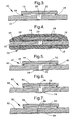
- FIGS 3 and 4 represent a circuit board assembly 10 before and after overmolding, respectively, in accordance with a first embodiment of this invention.
- the assembly 10 is shown as comprising a circuit board 12 having a surface to which a flip chip 14 is attached with solder connections 18, which are typically located along the entire perimeter of the chip 14.
- the circuit board 12 may be a laminate, printed wiring board (PWB), or any other suitable circuit board material known in the art.
- PWB printed wiring board
- a flip chip 14 is represented in Figures 3 and 4, the invention is applicable to essentially any surface-mount device, including BGA's, that is physically and electrically connected to a circuit board with solder connections formed by any suitable method, such as a solder bump reflow technique.
- Figures 3 and 4 also show a cavity 20 centrally located in the surface of the circuit board 12 beneath the flip chip 14.
- the cavity 20 is shown as being a blind hole beneath the chip 14, and serves to receive air trapped beneath the chip 14 during an underfill process, as depicted in Figure 4. More particularly, the cavity 20 is intended to accommodate air (or whatever gas may be present) during a molding process in which the chip 14 is underfilled while the circuit board 12 is simultaneously overmolded with the same molding material 16.
- the molding material 16 encases the circuit board 12 and chip 14, filling the gaps between the circuit board 12 and upper and lower molds (not shown) in which the molding operation is performed.
- the result is an overmolded housing 30 that forms a protective environmental seal around the circuit board 12 and chip 14.
- An object of the invention is that the molding material 16 not only fills the mold cavities on either side of the board 12, but also completely fills a gap 22 between the chip 14 and the board 12 created as a result of the solder connections 18 spacing the chip 14 above the surface of the board 12.
- the molding material 16 must readily flow during the overmolding/underfilling operation, and after curing have a suitable CTE relative to that of the board 12.
- Appropriate materials are thermosetting polymers such as epoxies to which a fine particulate fill material is added to achieve a CTE of about 12 to 17 ppm/°C.
- the fill material preferably has an average particle size of less than 1.0 mil (25 micrometers) to be sufficiently flowable during molding.
- Suitable compositions for the fill material are dependent on the particular thermosetting polymer used and the amount necessary to achieve the desired CTE.
- Particularly suitable overmold/underfill materials for the molding material 16 are thermoset epoxy resins to which about 80 to about 90 volume percent of silicon particles is admixed as a fill material.
- the flow of the molding material 16 during the molding operation is indicated by arrows in Figure 4.
- the molding material 16 is indicated as being injected into the mold cavity from the right-hand side of Figure 4, such that the molding material 16 flow is leftward across the top of the chip 14 and simultaneously between adjacent solder connections 18 along the near edge (the right edge in Figure 4) of the chip 14.
- the molding material 16 will advance leftward much more rapidly over and around the chip 14 than through the gap 22.
- the molding material 16 covers the edges of the chip 14 oriented parallel to the flow direction, the molding material 16 enters the gap 22 and flows toward the center of the chip 14.
- the cavity 20 isolates the entrapped air in a non-critical area of the circuit board 12, in that the air trapped within the cavity 20 does not contact the lower surface of the chip 14 and therefore does not have a detrimental effect on the thermal cycle life of the chip 14.
- the board 12 is much thicker than the gap 22 between the flip chip 14 and the board 12, such that the cavity 20 can accommodate an amount of air that would otherwise form a void with a much larger diameter than the cavity 20.
- the diameter of the cavity 20 required to accommodate the air without any compression would be only about 0.029 inch (about 0.74 mm).
- a cavity 20 of this size would not affect the thermal cycle reliability of the flip chip 14, based on experience with production flip chip designs that employ through-hole vias under the chip for interconnect and thermal dissipation functions.
- FIGs 5 through 7 represent three lower-cost approaches for forming a closed hole in a circuit board.
- Figures 5 and 6 make use of a single closed hole, while Figure 7 represents an embodiment in which multiple closed holes are used.
- a circuit board assembly 40 is shown as comprising a flip chip 44 attached with solder connections 48 to a circuit board 42, essentially in an identical manner to that of Figures 3 and 4.
- a cavity 50 is formed by closing a through-hole in the circuit board 42 with an adhesive tape 54 applied to the surface of the board 42 opposite the chip 44.
- Suitable tape materials for use in this embodiment include pressure-sensitive adhesive (PSA) tapes comprising acrylic adhesives on a polyimide film.
- PSA pressure-sensitive adhesive
- a circuit board assembly 60 is shown in which a cavity 70 is formed by closing a through-hole in a circuit board 62 with an adhesive compound 74 applied to the surface of the board 62 opposite a chip 64.
- a suitable compound 74 for this embodiment is an RTV or heat-curable silicone adhesive, an example of which is commercially available from Shin Etsu under the name X-832-161A.
- the adhesive compound 74 can be applied in any suitable manner prior to the overmolding/underfilling process.
- Figure 7 shows a circuit board assembly 80 in which multiple cavities 90 are formed by closing through-holes in a circuit board 82 with a solder mask 94 applied to the surface of the board 82 opposite a flip chip 84.
- the through-holes of Figure 7 can be sealed during typical circuit board manufacture, and with essentially any printed or film solder mask material. Since solder mask materials typically have relatively low mechanical strength as compared to an adhesive tape or compound, Figure 7 represents the cavities 90 as having relatively small diameters to prevent rupturing by trapped compressed air during the molding operation. Hence, multiple cavities 90 are required to accommodate a volume of air comparable to that which can be accommodated by the larger cavities 50 and 70 of Figures 5 and 6.
- 0.400 inch (about 1 mm) and 0.200 inch (about 0.5 mm) flip chips were mounted to a 0.047 inch (about 1.2 mm) thick circuit board in which cavities were formed by closing 0.015 and 0.030 inch (about 0.38 and 0.76 mm) diameter through-holes in the board with a PSA tape commercially available from 3M under the name KAPTON®.
- This PSA tape has an acrylic adhesive on a 0.003 inch (about 75 micrometers) thick polyimide backing.
- the chip was reflow soldered to the board in accordance with conventional practice to yield fine-pitch solder connections spaced about 0.008 inch (about 0.2 mm) apart, with a stand-off height (gap 52 in Figure 5) of about 0.003 inch (about 75 micrometers).
- the board and chip were simultaneously overmolded and underfilled, respectively, using a thermoset epoxy resin available from Plaskon under the name 200-302B, but then modified by the addition of about 80 to 90 volume percent of a silicon powder having an average particle size of less than 10 micrometers to achieve a viscosity of about 35 poise. Examination of the chip following the molding operation revealed that voids were not present anywhere in the underfill.
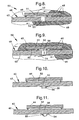
- Figures 8 and 9 illustrate additional features made possible with the embodiment represented in Figure 5.
- the adhesive tape 54 is pressed tightly against the circuit board 42 because the pressure is higher on the lower side of the board 42 as a result of the molding material 46 having a more advanced front along the lower surface of the board 42 as compared to the upper surface of the board 42.
- Such a situation can be expected because of the resistance to flow provided by a combination of the chip 44, the gap size, the number and size of other components on the board 42, and the mold gating.
- Figures 10 and 11 represent two additional embodiments of this invention that allow for more air volume to be accommodated in a through-hole closed by a tape.
- the tape 54 of Figure 5 has been modified to define a pocket 55 below the through-hole, thereby increasing the volume of the cavity 50.
- This embodiment is believed to benefit from the use of a more rigid tape 54 capable of maintaining the shape of the pocket 55.
- an acrylic adhesive on a thin metal (e.g., aluminum) film could be used as the tape 54.
- Figure 11 shows the tape 54 as being formed to have a sufficiently elastic backing material to allow the tape 54 to expand to accommodate a larger air volume, as indicated in phantom.
- An advantage of each of these embodiments is to allow the use of a smaller diameter cavity 50 in the circuit board 42 to accommodate a given volume of air.
Landscapes
- Encapsulation Of And Coatings For Semiconductor Or Solid State Devices (AREA)
- Wire Bonding (AREA)
Abstract
Description
Claims (20)
- An overmolded circuit board assembly comprising:a circuit board (12,42,62,82) having a first surface and an oppositely-disposed second surface;a surface-mount circuit device (14,44,64,84) attached to the first surface of the circuit board (12,42,62,82) with solder bump connections (18,48), the circuit device (14,44,64,84) being spaced above the first surface of the circuit board (12,42,62,82) by the solder bump connections (18,48) so as to define a gap (22,52,72,92) therebetween; anda cavity (20,50,70,90) defined in the circuit board (12,42,62,82) beneath the circuit device (14,44,64,84), the cavity (20,50,70,90) communicating with the gap (22,52,72,92) between the circuit board (12,42,62,82) and the circuit device (14,44,64,84) and being closed off from the second surface of the circuit board (12,42,62,82).
- An overmolded circuit board assembly according to claim 1, further comprising a molding material (16,46) that completely fills the gap (22,52,72,92) between the circuit board (12,42,62,82) and the circuit device (14,44,64,84) and encapsulates the circuit device (14,44,64,84) and the circuit board (12,42,62,82) at the first and second surfaces thereof, wherein the cavity (20,50,70,90) contains pressurized gas.
- An overmolded circuit board assembly according to claim 1, wherein the cavity (20) is defined by a blind hole (20) in the first surface of the circuit board (12)
- An overmolded circuit board assembly according to claim 1, wherein the cavity (50,70,90) is defined by a through-hole in the circuit board (42,62,82) that is closed with a material (54,74,94) applied to the second surface of the circuit board (12,42,62,82).
- An overmolded circuit board assembly according to claim 4, wherein the material (54,74,94) is an adhesive tape (54) applied to the second surface of the circuit board (42)
- An overmolded circuit board assembly according to claim 5, wherein the adhesive tape (54) is bonded to the second surface of the circuit board (42) so that a portion of the adhesive tape (54) is deflectable from the second surface to enable venting of air from the first surface of the circuit board (42) to the second surface thereof.
- An overmolded circuit board assembly according to claim 5, wherein the adhesive tape (54) comprises a pocket (55) or is deformable to define a pocket (55) that increases the volume of the cavity (50).
- An overmolded circuit board assembly according to claim 4, wherein the material (54,74,94) is an adhesive compound (74) applied to the second surface of the circuit board (62).
- An overmolded circuit board assembly according to claim 4, wherein the material (54,74,94) is a solder mask layer (94) applied to the second surface of the circuit board (82).
- An overmolded circuit board assembly according to claim 1, wherein there are a plurality of cavities (90) in the first surface of the circuit board (82), each of the cavities (90) communicating with the gap (92) between the circuit board (82) and the circuit device (84).
- A method of forming an overmolded circuit board assembly, the method comprising the steps of:providing a circuit board (12,42,62,82) having a first surface, an oppositely-disposed second surface, and a cavity (20,50,70,90) defined in the circuit board (12,42,62,82), the cavity (20,50,70,90) communicating with the first surface of the circuit board (12,42,62,82) and being closed off from the second surface of the circuit board (12,42,62,82); andmounting a surface-mount circuit device (14,44,64,84) with solder bump connections (18,48) to the first surface of the circuit board (12,42,62,82) so that the cavity (20,50,70,90) is beneath the circuit device (14,44,64,84), the circuit device (14,44,64,84) being spaced above the first surface of the circuit board (12,42,62,82) by the solder bump connections (18,48) so as to define a gap (22,52,72,92) therebetween that communicates with the cavity (20,50,70,90).
- A method according to claim 11, further comprising the step of encapsulating the circuit device (14,44,64,84) and the circuit board (12,42,62,82) at the first and second surfaces thereof with a molding material (16,46), and completely filling the gap (22,52,72,92) between the circuit board (12,42,62,82) and the circuit device (14,44,64,84) with the molding material (16,46), the molding material (18,48) flowing in the gap (22,52,72,92) so as to compress a gas within the cavity (20,50,70,90).
- A method according to claim 11, wherein the cavity (20) is defined by forming a blind hole (20) in the first surface of the circuit board (12).
- A method according to claim 11, wherein the cavity (50,70,90) is defined by forming a through-hole in the circuit board (42,62,82), and then closing the through-hole with a material (54,74,94) applied to the second surface of the circuit board (42,62,82).
- A method according to claim 14, wherein the material (54,74,94) is an adhesive tape (54) applied to the second surface of the circuit board (42).
- A method according to claim 15, wherein the adhesive tape (54) is bonded to the second surface of the circuit board (42) so that a portion of the adhesive tape (54) is deflectable from the second surface, and the adhesive tape (54) deflects as the molding material (46) fills the gap (52) between the circuit board (42) and the circuit device (44) to enable venting of a gas from the first surface of the circuit board (42) to the second surface thereof.
- A method according to claim 15, wherein the adhesive tape (54) comprises a pocket (55) that increases the volume of the cavity (50) or is deformable to define a pocket (55) as the molding material (46) fills the gap (52) between the circuit board (42) and the circuit device (44) to increase the volume of the cavity (50) as gas is forced under pressure into the cavity (50).
- A method according to claim 14, wherein the material (54,74,94) is an adhesive compound (74) applied to the second surface of the circuit board (62).
- A method according to claim 14, wherein the material (54,74,94) is a solder mask layer (94) applied to the second surface of the circuit board (82).
- A method according to claim 11, wherein there are a plurality of cavities (90) in the first surface of the circuit board (82), each of the plurality of cavities (90) communicating with the gap (92) between the circuit board (82) and the circuit device (84).
Applications Claiming Priority (2)
| Application Number | Priority Date | Filing Date | Title |
|---|---|---|---|
| US09/948,147 US6693239B2 (en) | 2001-09-06 | 2001-09-06 | Overmolded circuit board with underfilled surface-mount component and method therefor |
| US948147 | 2001-09-06 |
Publications (3)
| Publication Number | Publication Date |
|---|---|
| EP1291912A2 true EP1291912A2 (en) | 2003-03-12 |
| EP1291912A3 EP1291912A3 (en) | 2005-01-12 |
| EP1291912B1 EP1291912B1 (en) | 2008-07-30 |
Family
ID=25487359
Family Applications (1)
| Application Number | Title | Priority Date | Filing Date |
|---|---|---|---|
| EP02078469A Expired - Lifetime EP1291912B1 (en) | 2001-09-06 | 2002-08-21 | Overmolded circuit board with underfilled surface-mount component and method therefor |
Country Status (3)
| Country | Link |
|---|---|
| US (1) | US6693239B2 (en) |
| EP (1) | EP1291912B1 (en) |
| DE (1) | DE60227890D1 (en) |
Cited By (1)
| Publication number | Priority date | Publication date | Assignee | Title |
|---|---|---|---|---|
| WO2007015683A1 (en) * | 2005-08-04 | 2007-02-08 | Infineon Technologies Ag | An integrated circuit package and a method for forming an integrated circuit package |
Families Citing this family (19)
| Publication number | Priority date | Publication date | Assignee | Title |
|---|---|---|---|---|
| US7339276B2 (en) * | 2002-11-04 | 2008-03-04 | Intel Corporation | Underfilling process in a molded matrix array package using flow front modifying solder resist |
| US6991969B2 (en) * | 2003-02-19 | 2006-01-31 | Octavian Scientific, Inc. | Methods and apparatus for addition of electrical conductors to previously fabricated device |
| US20050011672A1 (en) * | 2003-07-17 | 2005-01-20 | Alawani Ashish D. | Overmolded MCM with increased surface mount component reliability |
| US7553680B2 (en) * | 2004-08-09 | 2009-06-30 | Delphi Technologies, Inc. | Methods to provide and expose a diagnostic connector on overmolded electronic packages |
| US7230829B2 (en) * | 2005-01-28 | 2007-06-12 | Delphi Technologies, Inc. | Overmolded electronic assembly with insert molded heat sinks |
| US7422448B2 (en) * | 2005-07-28 | 2008-09-09 | Delphi Technologies, Inc. | Surface mount connector |
| US7579215B2 (en) * | 2007-03-30 | 2009-08-25 | Motorola, Inc. | Method for fabricating a low cost integrated circuit (IC) package |
| US20100066395A1 (en) | 2008-03-13 | 2010-03-18 | Johnson Morgan T | Wafer Prober Integrated With Full-Wafer Contacter |
| US8342228B2 (en) * | 2008-11-24 | 2013-01-01 | Apple Inc. | Systems and methods for insert-molding |
| US7999197B1 (en) * | 2009-04-20 | 2011-08-16 | Rf Micro Devices, Inc. | Dual sided electronic module |
| KR101934917B1 (en) * | 2012-08-06 | 2019-01-04 | 삼성전자주식회사 | Semiconductor Packages and Methods of Fabricating the Same |
| JP6044473B2 (en) * | 2013-06-28 | 2016-12-14 | 株式会社デンソー | Electronic device and method for manufacturing the same |
| JP7135293B2 (en) * | 2017-10-25 | 2022-09-13 | 富士電機株式会社 | Semiconductor device and method for manufacturing semiconductor device |
| US10971439B2 (en) * | 2018-02-22 | 2021-04-06 | Hamilton Sundstrand Corporation | Ball grid array underfilling systems |
| US11152295B2 (en) * | 2018-04-13 | 2021-10-19 | Taiwan Semiconductor Manufacturing Company Ltd. | Semiconductor package structure and method for manufacturing the same |
| DE102019215696A1 (en) * | 2019-10-11 | 2021-04-15 | Continental Teves Ag & Co. Ohg | Electronics unit with improved cooling |
| CN113394118B (en) * | 2020-03-13 | 2022-03-18 | 长鑫存储技术有限公司 | Package structure and method of forming the same |
| CN217405408U (en) * | 2021-03-22 | 2022-09-09 | 意法半导体(格勒诺布尔2)公司 | Electronic device and electronic system |
| FR3120987B1 (en) * | 2021-03-22 | 2023-05-26 | St Microelectronics Grenoble 2 | CHIP PACKAGING DEVICE AND METHOD FOR MAKING THE SAME |
Family Cites Families (8)
| Publication number | Priority date | Publication date | Assignee | Title |
|---|---|---|---|---|
| US5612576A (en) * | 1992-10-13 | 1997-03-18 | Motorola | Self-opening vent hole in an overmolded semiconductor device |
| US5385869A (en) * | 1993-07-22 | 1995-01-31 | Motorola, Inc. | Semiconductor chip bonded to a substrate and method of making |
| US5710071A (en) * | 1995-12-04 | 1998-01-20 | Motorola, Inc. | Process for underfilling a flip-chip semiconductor device |
| US6038136A (en) * | 1997-10-29 | 2000-03-14 | Hestia Technologies, Inc. | Chip package with molded underfill |
| JP2000150730A (en) * | 1998-11-17 | 2000-05-30 | Fujitsu Ltd | Semiconductor device and manufacturing method thereof |
| US6490166B1 (en) * | 1999-06-11 | 2002-12-03 | Intel Corporation | Integrated circuit package having a substrate vent hole |
| JP2001044137A (en) * | 1999-08-04 | 2001-02-16 | Hitachi Ltd | Electronic device and method of manufacturing the same |
| US6519844B1 (en) * | 2001-08-27 | 2003-02-18 | Lsi Logic Corporation | Overmold integrated circuit package |
-
2001
- 2001-09-06 US US09/948,147 patent/US6693239B2/en not_active Expired - Lifetime
-
2002
- 2002-08-21 DE DE60227890T patent/DE60227890D1/en not_active Expired - Lifetime
- 2002-08-21 EP EP02078469A patent/EP1291912B1/en not_active Expired - Lifetime
Cited By (2)
| Publication number | Priority date | Publication date | Assignee | Title |
|---|---|---|---|---|
| WO2007015683A1 (en) * | 2005-08-04 | 2007-02-08 | Infineon Technologies Ag | An integrated circuit package and a method for forming an integrated circuit package |
| US8357565B2 (en) | 2005-08-04 | 2013-01-22 | Infinenon Technologies Ag | Integrated circuit package and a method for forming an integrated circuit package |
Also Published As
| Publication number | Publication date |
|---|---|
| US6693239B2 (en) | 2004-02-17 |
| DE60227890D1 (en) | 2008-09-11 |
| EP1291912B1 (en) | 2008-07-30 |
| US20030042035A1 (en) | 2003-03-06 |
| EP1291912A3 (en) | 2005-01-12 |
Similar Documents
| Publication | Publication Date | Title |
|---|---|---|
| US6693239B2 (en) | Overmolded circuit board with underfilled surface-mount component and method therefor | |
| EP1432033B1 (en) | Multi-chip module and method of forming | |
| US6521480B1 (en) | Method for making a semiconductor chip package | |
| US6307749B1 (en) | Overmolded electronic module with underfilled surface-mount components | |
| US9269648B2 (en) | Thermally enhanced package with lid heat spreader | |
| US6724080B1 (en) | Heat sink with elevated heat spreader lid | |
| US6157086A (en) | Chip package with transfer mold underfill | |
| US6038136A (en) | Chip package with molded underfill | |
| US6987058B2 (en) | Methods for underfilling and encapsulating semiconductor device assemblies with a single dielectric material | |
| US7348218B2 (en) | Semiconductor packages and methods of manufacturing thereof | |
| CN101266962B (en) | Semiconductor device and method of manufacturing the same | |
| CN1452245A (en) | Semiconductor device and manufacturing method thereof | |
| CN104051395A (en) | Chip package-in-package and method thereof | |
| US7790510B1 (en) | Metal lid with improved adhesion to package substrate | |
| JP2004072009A (en) | Semiconductor device and manufacturing method thereof | |
| US20080298023A1 (en) | Electronic component-containing module and manufacturing method thereof | |
| US10896877B1 (en) | System in package with double side mounted board | |
| US7122407B2 (en) | Method for fabricating window ball grid array semiconductor package | |
| US20050093181A1 (en) | Heat sinkable package | |
| US8004069B2 (en) | Lead frame based semiconductor package and a method of manufacturing the same | |
| US7432601B2 (en) | Semiconductor package and fabrication process thereof | |
| TWI658518B (en) | Method for manufacturing circuit part and circuit part | |
| JP2001144230A (en) | Semiconductor device and manufacturing method thereof | |
| US20060273467A1 (en) | Flip chip package and method of conducting heat therefrom | |
| US7999197B1 (en) | Dual sided electronic module |
Legal Events
| Date | Code | Title | Description |
|---|---|---|---|
| PUAI | Public reference made under article 153(3) epc to a published international application that has entered the european phase |
Free format text: ORIGINAL CODE: 0009012 |
|
| AK | Designated contracting states |
Kind code of ref document: A2 Designated state(s): AT BE BG CH CY CZ DE DK EE ES FI FR GB GR IE IT LI LU MC NL PT SE SK TR Designated state(s): AT BE BG CH CY CZ DE DK EE ES FI FR GB GR IE IT LI LU MC NL PT SE SK TR |
|
| AX | Request for extension of the european patent |
Extension state: AL LT LV MK RO SI |
|
| PUAL | Search report despatched |
Free format text: ORIGINAL CODE: 0009013 |
|
| AK | Designated contracting states |
Kind code of ref document: A3 Designated state(s): AT BE BG CH CY CZ DE DK EE ES FI FR GB GR IE IT LI LU MC NL PT SE SK TR |
|
| AX | Request for extension of the european patent |
Extension state: AL LT LV MK RO SI |
|
| RIC1 | Information provided on ipc code assigned before grant |
Ipc: 7H 01L 23/31 A Ipc: 7H 01L 21/56 B |
|
| 17P | Request for examination filed |
Effective date: 20050712 |
|
| AKX | Designation fees paid |
Designated state(s): DE FR GB |
|
| GRAP | Despatch of communication of intention to grant a patent |
Free format text: ORIGINAL CODE: EPIDOSNIGR1 |
|
| GRAS | Grant fee paid |
Free format text: ORIGINAL CODE: EPIDOSNIGR3 |
|
| GRAA | (expected) grant |
Free format text: ORIGINAL CODE: 0009210 |
|
| AK | Designated contracting states |
Kind code of ref document: B1 Designated state(s): DE FR GB |
|
| REG | Reference to a national code |
Ref country code: GB Ref legal event code: FG4D |
|
| REF | Corresponds to: |
Ref document number: 60227890 Country of ref document: DE Date of ref document: 20080911 Kind code of ref document: P |
|
| PLBE | No opposition filed within time limit |
Free format text: ORIGINAL CODE: 0009261 |
|
| STAA | Information on the status of an ep patent application or granted ep patent |
Free format text: STATUS: NO OPPOSITION FILED WITHIN TIME LIMIT |
|
| 26N | No opposition filed |
Effective date: 20090506 |
|
| REG | Reference to a national code |
Ref country code: FR Ref legal event code: PLFP Year of fee payment: 14 |
|
| REG | Reference to a national code |
Ref country code: FR Ref legal event code: PLFP Year of fee payment: 15 |
|
| REG | Reference to a national code |
Ref country code: FR Ref legal event code: PLFP Year of fee payment: 16 |
|
| REG | Reference to a national code |
Ref country code: FR Ref legal event code: PLFP Year of fee payment: 17 |
|
| REG | Reference to a national code |
Ref country code: DE Ref legal event code: R082 Ref document number: 60227890 Country of ref document: DE Representative=s name: MANITZ FINSTERWALD PATENT- UND RECHTSANWALTSPA, DE Ref country code: DE Ref legal event code: R081 Ref document number: 60227890 Country of ref document: DE Owner name: DELPHI TECHNOLOGIES IP LIMITED, BB Free format text: FORMER OWNER: DELPHI TECHNOLOGIES, INC., TROY, MICH., US |
|
| REG | Reference to a national code |
Ref country code: GB Ref legal event code: 732E Free format text: REGISTERED BETWEEN 20190214 AND 20190221 |
|
| PGFP | Annual fee paid to national office [announced via postgrant information from national office to epo] |
Ref country code: FR Payment date: 20210825 Year of fee payment: 20 |
|
| PGFP | Annual fee paid to national office [announced via postgrant information from national office to epo] |
Ref country code: GB Payment date: 20210827 Year of fee payment: 20 Ref country code: DE Payment date: 20210827 Year of fee payment: 20 |
|
| REG | Reference to a national code |
Ref country code: DE Ref legal event code: R071 Ref document number: 60227890 Country of ref document: DE |
|
| REG | Reference to a national code |
Ref country code: GB Ref legal event code: PE20 Expiry date: 20220820 |
|
| PG25 | Lapsed in a contracting state [announced via postgrant information from national office to epo] |
Ref country code: GB Free format text: LAPSE BECAUSE OF EXPIRATION OF PROTECTION Effective date: 20220820 |