EP1289145A2 - Frequency correcting method for cellular phone terminal - Google Patents
Frequency correcting method for cellular phone terminal Download PDFInfo
- Publication number
- EP1289145A2 EP1289145A2 EP02256047A EP02256047A EP1289145A2 EP 1289145 A2 EP1289145 A2 EP 1289145A2 EP 02256047 A EP02256047 A EP 02256047A EP 02256047 A EP02256047 A EP 02256047A EP 1289145 A2 EP1289145 A2 EP 1289145A2
- Authority
- EP
- European Patent Office
- Prior art keywords
- frequency
- oscillation circuit
- base station
- crystal oscillation
- signal
- Prior art date
- Legal status (The legal status is an assumption and is not a legal conclusion. Google has not performed a legal analysis and makes no representation as to the accuracy of the status listed.)
- Withdrawn
Links
- 230000001413 cellular effect Effects 0.000 title claims abstract description 41
- 238000000034 method Methods 0.000 title claims description 9
- 239000013078 crystal Substances 0.000 claims abstract description 90
- 230000010355 oscillation Effects 0.000 claims abstract description 82
- 238000004891 communication Methods 0.000 claims abstract description 16
- 238000012937 correction Methods 0.000 claims description 15
- 238000012545 processing Methods 0.000 claims description 11
- 238000010586 diagram Methods 0.000 description 9
- 238000010276 construction Methods 0.000 description 5
- 230000003111 delayed effect Effects 0.000 description 4
- 238000005259 measurement Methods 0.000 description 4
- 238000010295 mobile communication Methods 0.000 description 3
- 230000005540 biological transmission Effects 0.000 description 1
- 238000006243 chemical reaction Methods 0.000 description 1
- 238000000691 measurement method Methods 0.000 description 1
Images




Classifications
-
- H—ELECTRICITY
- H04—ELECTRIC COMMUNICATION TECHNIQUE
- H04B—TRANSMISSION
- H04B7/00—Radio transmission systems, i.e. using radiation field
- H04B7/24—Radio transmission systems, i.e. using radiation field for communication between two or more posts
- H04B7/26—Radio transmission systems, i.e. using radiation field for communication between two or more posts at least one of which is mobile
-
- H—ELECTRICITY
- H03—ELECTRONIC CIRCUITRY
- H03J—TUNING RESONANT CIRCUITS; SELECTING RESONANT CIRCUITS
- H03J7/00—Automatic frequency control; Automatic scanning over a band of frequencies
- H03J7/02—Automatic frequency control
- H03J7/04—Automatic frequency control where the frequency control is accomplished by varying the electrical characteristics of a non-mechanically adjustable element or where the nature of the frequency controlling element is not significant
- H03J7/08—Automatic frequency control where the frequency control is accomplished by varying the electrical characteristics of a non-mechanically adjustable element or where the nature of the frequency controlling element is not significant using varactors, i.e. voltage variable reactive diodes
-
- H—ELECTRICITY
- H03—ELECTRONIC CIRCUITRY
- H03J—TUNING RESONANT CIRCUITS; SELECTING RESONANT CIRCUITS
- H03J1/00—Details of adjusting, driving, indicating, or mechanical control arrangements for resonant circuits in general
- H03J1/0008—Details of adjusting, driving, indicating, or mechanical control arrangements for resonant circuits in general using a central processing unit, e.g. a microprocessor
-
- H—ELECTRICITY
- H03—ELECTRONIC CIRCUITRY
- H03L—AUTOMATIC CONTROL, STARTING, SYNCHRONISATION OR STABILISATION OF GENERATORS OF ELECTRONIC OSCILLATIONS OR PULSES
- H03L1/00—Stabilisation of generator output against variations of physical values, e.g. power supply
Definitions
- the present invention relates to a cellular phone terminal with which the reception frequency is corrected on the basis of a reference signal transmitted from a base station, and to a frequency correcting method for the cellular phone terminal.
- TCXO Temporal-Compensated Crystal Oscillator
- the present invention has an object to enable use of an inexpensive crystal oscillation circuit having a low frequency-error precision in a cellular phone terminal.
- a frequency correcting method in a cellular phone terminal for communicating a radio signal with a base station comprising: a first step of receiving a reference signal for correcting the reception frequency of the radio signal transmitted from the base station after powered on; a second step of correcting the reception frequency on the basis of the reference signal received through the processing of the first step; and a third step of making normal communications with the base station after the processing of the second step.
- a frequency correcting method in a cellular phone terminal for communicating a radio signal with a base station comprising: a first step of receiving a reference signal for correcting the reception frequency of the radio signal transmitted from the base station when the cellular phone terminal is on standby.; a second step of correcting the reception frequency on the basis of the reference signal received through the processing of the first step; and a third step of shifting to the normal communications with the base station after the processing of the second step.
- a cellular phone terminal for communicating a radio signal with a base station, comprising: a radio reception portion for receiving the radio signal transmitted from the base station and demodulating the received radio signal, a base band portion for measuring the frequency error of the demodulated signal, a crystal oscillation circuit portion, control means for bringing the frequency of the frequency signal outputted from the crystal oscillation circuit portion into correspondence with the frequency of a reference signal, the reference signal correcting the reception frequency of the radio signal, first frequency correction portion for supplying the crystal oscillation circuit portion with the voltage for correcting the frequency error outputted from the base band portion while receiving the reference signal transmitted from the base station, second frequency correction portion for supplying the crystal oscillation circuit portion with the voltage for correcting the frequency error outputted from the base band portion under the normal communications which the radio reception portion receives the radio signal, and synthesizer portions for correcting the frequency error of the radio reception portion on the basis of the frequency signal outputted from the crystal oscillation circuit portion.
- Fig. 1 is a diagram showing a frequency band used by a cellular phone terminal to which the present invention is applied.
- the cellular phone terminal is used in a next-generation mobile communication system called as "IMT 2000 (International Mobile Communication 2000)". As shown in Fig.
- 5 MHz (from 1920 to 1925 MHz) band serving as a guard band (buffer band) for preventing interference from PHS (Personal Handyphone System; PHS is developed on the basis of a digital code-less phone in Japan)
- 5 MHz (from 1940 to 1945 MHz, from 1960 to 1965 MHz) bands serving as guard bands as a result of pursuance carried out from the standpoint of fairness
- 15 MHz from 1925 to 1940 MHz, 15 MHz from 1945 to 1960 MHz and 15MHz from 1965 to 1980 MHz are allocated as the transmission frequency band (that is, up frequency band) in the cellular phone terminal
- 15 MHz from 2115 to 2130 MHz, 15 MHz from 2135 to 2150 MHz and 15 MHz from 2155 to 2170 MHz are allocated as the reception frequency band (that is, down frequency band) in the cellular phone terminal.
- the cellular phone terminal is equipped with a crystal oscillation circuit comprising a crystal oscillator which is cheaper than TCXO (Temperature Compensated Crystal Oscillator) generally used in a cellular phone terminal, but has less frequency precision than TCXO, and AFC (Automatic Frequency Control) circuit for the crystal oscillation circuit for performing the frequency correction of the crystal oscillation circuit.
- TCXO Tempoture Compensated Crystal Oscillator
- AFC Automatic Frequency Control
- a non-modulated reference frequency signal (reference signal) for correction of a crystal oscillation circuit is transmitted from a base station into the guard band 5 MHz of the reception frequency for the cellular phone terminal, for example, high-precision non-modulated waves (signal) of 2132.5 MHz are transmitted from a base station (not shown) at all times, the signal of 2132.5 MHz is received as a reference frequency for correcting the crystal oscillation circuit when the cellular phone terminal is powered on, and the AFC circuit for the crystal oscillation circuit corrects the frequency of the crystal oscillation circuit on the basis of the reference frequency for correcting the crystal oscillation circuit.
- Fig. 2 is a block diagram showing the construction of the main part of the cellular phone terminal.
- the cellular phone terminal comprises radio reception portion 10 containing an antenna, a duplexer, LNA (Low Noise Amplifier), a RF band bass filter, an IF mixer, an IF band pass filter and a demodulator, base band portion 20 for performing power measurement of desired signals I, Q and calculation of a frequency error, down-conversion PLL synthesizer portion 30 containing VCO (Voltage Controlled Oscillator) and a loop filter, demodulation PLL synthesizer portion 40 containing VCO and a loop filter, crystal oscillation circuit portion 50 comprising a crystal oscillator for supplying a reference frequency to the PLL synthesizer portions 30 and 40, an AFC portion 60 for the crystal oscillation circuit which supplies the crystal oscillation circuit portion 50 with the voltage corresponding to the frequency error value calculated and outputted by the base band portion 20, an AFC portion 70, and CPU portion 80 for controlling the radio reception portion 10, the base band portion 20, the PLL synthesizer portions 30 and 40, the AFC portion 60 for
- Fig. 4 is a diagram showing the internal construction of the crystal oscillation circuit portion 50.
- the crystal oscillation circuit portion 50 comprises resistor R1, crystal oscillator Cr, capacitance-variable diode D and an oscillating circuit device 50A.
- the oscillating circuit device 50A is constructed as shown in the equivalent circuit diagram of Fig. 5. That is, the oscillating circuit device 50A comprises resistor R2 and capacitance CL.
- Fig. 6 is a graph showing the relationship between voltage error ⁇ V and frequency error ⁇ f in the crystal oscillation circuit portion 50.
- the voltage error inputted to the crystal oscillation circuit portion 50 and the frequency error outputted from the crystal oscillation circuit portion 50 are in direct proportion to each other as shown in Fig. 6.
- Voltage error ⁇ V1 and frequency error ⁇ f1 are one voltage error value and one frequency error value, respectively.
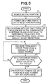
- Fig. 3 is a flowchart showing the operation when the voltage value outputted from the AFC portion 60 for the crystal oscillation circuit to the crystal oscillation circuit portion 50 on the basis of the reference frequency for the correction of the crystal oscillation circuit is adjusted to correct the output frequency of the crystal oscillation circuit portion 50.
- the operation of an embodiment according to the method of the present invention will be described hereunder with reference to the flowchart of Fig. 3 and Figs. 2 to 8.
- the power source switch (not shown) of the cellular phone terminal When the power source switch (not shown) of the cellular phone terminal is turned on in step S1 of Fig. 3, the power source for CPU portion 80 is turned on, so that power is supplied to the CPU portion 80.
- the power source for the radio reception portion 10 the base band portion 20, the PLL synthesizer portions 30 and 40, the crystal oscillation circuit portion 50 and the AFC portion 60 for the crystal oscillation circuit is turned on in step S2.
- step S3 the CPU portion 80 matches local frequencies for reception corresponding to the outputs of the PLL synthesizer portions 30 and 40 with the reference frequency for the crystal oscillation circuit transmitted from a base station (not shown) to start the reception of radio signals transmitted from the base station. That is, if the reference frequency for the crystal oscillation circuit transmitted from the base station is equal to 2132 MHz for example, the CPU portion 80 supplies the crystal oscillation circuit portion 50 with such a voltage value that the output frequency of the crystal oscillation circuit portion 50 is equal to 2132 MHz, thereby setting the output frequency to 2132 MHz.
- the output frequency of the PLL synthesizer portion 30 is set to about 2512 MHz
- the output frequency of the PLL synthesizer portion 40 is set to about 380 MHz.
- the radio reception portion 10 receives and demodulates the radio signals from the base station side on the basis of the output frequencies from the PLL synthesizer portions 30, 40, and demodulates, and outputs the demodulation signal. In this case, the output of the radio reception portion 10, that is, the demodulated signals I, Q become direct current or sine wave of low frequency occurring due to a frequency error of the crystal oscillation circuit portion 50.
- step S4 the base band portion 20 measures the frequency errors of the signals I, Q (I, Q signals) demodulated by the radio reception portion 10 according to a measurement method described later.
- step S5 the AFC portion 60 for the crystal oscillation circuit is supplied with the frequency error measured by the base band portion 20, and varies a crystal-oscillation-circuit controlling voltage according to the frequency error. That is, the AFC portion 60 for the crystal oscillation circuit supplies the crystal oscillating circuit portion 50 with the crystal-oscillation-circuit controlling voltage with which the frequency error is corrected.
- the oscillation frequency whose frequency error is equal to "0" is outputted from the crystal oscillating circuit portion 50, and the signals having a frequency whose frequency error is equal to "0" are outputted from the PLL synthesizer portions 30, 40 in which the signals of the frequency corresponding to the output of the crystal oscillation circuit portion 50 are generated.
- N max a preset number of times
- the CPU portion 80 recognizes that the reception frequency of the radio reception portion 10 has been sufficiently corrected. Therefore, the CPU portion 80 powers on the AFC portion 70 and powers off the AFC portion 60 for the crystal oscillation circuit in step S6, thereby shifting to the normal communication state under the control of the AFC portion 70.
- the difference signal between the following first and second signals is output from the base band portion 20. That is, the signal Q is delayed by a time ⁇ in delay portion 20B, and then the signal Q thus delayed by the time ⁇ is mixed with the signal I in multiplier 20C to achieve the first signal. Further, the signal I is delayed by a time ⁇ in delay portion 20A, and then the signal I thus delayed by the time ⁇ is mixed with the signal Q in multiplier 20D to achieve the second signal.
- the difference signal between the following first and second signals is output from subtracter 20E.
- the difference ⁇ between the first and second signals can be represented by the following equation (1).
- ⁇ cos ⁇ t ⁇ sin ⁇ ( t + ⁇ )-sin ⁇ t ⁇ cos ⁇ ( t + ⁇ )
- the difference ⁇ between the first and second signals has a characteristic as shown in the graph of Fig. 8, and this value increases as the frequency error ⁇ f is increased.
- the AFC portion 60 for the crystal oscillation circuit outputs to the crystal oscillation circuit portion 50 the voltage value for correcting the frequency error ⁇ f corresponding to the measurement value. Accordingly, such a frequency signal that the frequency error ⁇ f is equal to "0" is output from the crystal oscillation circuit portion 50, so that such frequency signals that the frequency error ⁇ f is equal to "0" are also outputted from the PLL synthesizer portions 30, 40. Accordingly, the frequency error of the radio reception portion 10 for receiving and demodulating the radio signals on the basis of the output frequencies of the PLL synthesizer portions 30, 40 is also equal to "0".
- the AFC portion 60 for the crystal oscillation circuit corrects the frequency of the crystal oscillation circuit portion 50 on the basis of the non-modulated reference frequency for the correction of the crystal oscillation circuit when the cellular phone terminal is powered on, and after the correction, the AFC portion 60 for the crystal oscillation circuit is switched to the AFC portion 70 to shift the communication state to the normal communication state. Therefore, the relatively cheap crystal oscillation circuit portion 50 can be used for the cellular phone terminal as a replacement for TCXO. Further, by performing the frequency correction on the basis of the reference frequency for correcting the crystal oscillation circuit, a temperature compensated circuit in TCXO may be omitted.
- the frequency of the crystal oscillation circuit portion 50 is corrected when the cellular phone terminal is powered on.
- the frequency error of the crystal oscillation circuit portion 50 which is caused by temperature variation of the cellular phone terminal is periodically corrected when the AFC portion 60 for the crystal oscillation circuit is on standby.
- Fig. 9 is a graph showing the relationship between the temperature and the frequency error of the crystal oscillation circuit having no temperature compensated circuit.
- Fig. 10 is a graph showing the relationship between the temperature and the frequency error of TCXO (Temperature Compensated Crystal Oscillator) having a temperature compensating circuit. From the graphs of Figs. 9 and 10, it is apparent that the variation of the frequency error caused by the temperature variation of the crystal oscillation circuit having no temperature compensating circuit is large.
- TCXO Tempoture Compensated Crystal Oscillator
- Fig. 11 is a flowchart showing the correction operation of the frequency by the AFC portion 60 for the crystal oscillation circuit when the cellular phone terminal is on standby.
- step S11 of Fig. 11 when the cellular phone terminal is on standby, the CPU portion 80 powers off the AFC portion 70 and powers on the AFC portion 60 for the crystal oscillation circuit.
- the base band portion 20 measures the frequency errors of the demodulated signals I, Q of the radio reception portion 10 for receiving and demodulating the radio signals on the basis of the output frequencies of the PLL synthesizer portions 30, 40 which are based on the reference frequency for the crystal oscillation circuit from the base station.
- step S13 the AFC portion 60 for the crystal oscillation circuit is supplied with the frequency error measured by the base band portion 20 and varies the crystal-oscillation-circuit controlling voltage in accordance with the frequency error thus supplied. That is, the AFC portion 60 for the crystal oscillation circuit supplies the crystal oscillation circuit portion 50 with the crystal-oscillation-circuit controlling voltage with which the frequency error is corrected.
- the frequency errors of the demodulated signals I, Q (I, Q signals) of the radio reception portion 10 for receiving and demodulating the radio signals on the basis of the output frequencies of the PLL synthesizer portions 30, 40 are set to "0" by repetitively executing each processing of the steps S12, S13 described above at a preset number of times.
- the CPU portion 80 judges that the reception frequency of the radio reception portion 10 has been sufficiently corrected, so that it powers on the AFC portion 70 and powers off the AFC portion 60 for the crystal oscillation circuit in step S14, thereby shifting to the normal communication state under the control of the AFC portion 70.
- the AFC portion 70 is switched to the AFC portion 60 for the crystal oscillation circuit when the cellular phone terminal is on standby, and the frequency correction is carried out by the AFC portion 60 for the crystal oscillation circuit. After this correction, the AFC portion 60 for the crystal oscillation circuit is switched to the AFC portion 70 to shift the communication state to the normal communication state.
- the AFC portion 70 is switched to the AFC portion 60 for the crystal oscillation circuit to perform the frequency correction.
- a cellular phone terminal When a cellular phone terminal is powered on, it immediately receives a reference signal (non-modulated reference frequency signal for correcting a crystal oscillation circuit) for correcting the reception frequency of a radio signal transmitted from a base station at all times, and corrects the error of the reception frequency on the basis of the reference signal received. After the error of the reception frequency is corrected, the cellular phone terminal makes normal communications with the base station.
- a reference signal non-modulated reference frequency signal for correcting a crystal oscillation circuit
Landscapes
- Engineering & Computer Science (AREA)
- Computer Hardware Design (AREA)
- Microelectronics & Electronic Packaging (AREA)
- Computer Networks & Wireless Communication (AREA)
- Signal Processing (AREA)
- Transceivers (AREA)
- Circuits Of Receivers In General (AREA)
- Oscillators With Electromechanical Resonators (AREA)
- Mobile Radio Communication Systems (AREA)
Abstract
Description
Claims (8)
- A frequency correcting method in a cellular phone terminal for communicating via a radio signal with a base station, comprising:a first step of receiving a reference signal transmitted from said base station for correcting an oscillator frequency of the terminal;a second step of correcting the oscillator frequency on the basis of the reference signal; anda third step of making normal communication with said base station after the processing of said second step.
- The method as claimed in claim 1 wherein said reference signal is received upon powering up of said terminal.
- The method according to claim 1 or claim 2 wherein said reference signal is received when said terminal is on standby.
- The method as claimed in any one of the preceding claims wherein the reference signal is transmitted as a non - modulated signal from the base station using a non - communication buffer area about the radio signal.
- A cellular phone terminal for communicating via a radio signal with a base station, comprising:means for receiving a reference signal transmitted from said base station for correcting an oscillator frequency of the terminal;means for correcting the oscillator frequency on the basis of the reference signal; andmeans for making normal communication with said base station using said corrected oscillator frequency.
- A cellular phone terminal as claimed in claim 5, comprising:a radio reception portion for receiving the radio signal transmitted from said base station and demodulating the received radio signal;a base band portion for measuring the frequency error of the demodulated signal;a crystal oscillation circuit portion;control means for bringing the frequency signal outputted from said crystal oscillation circuit portion into correspondence with the frequency of the reference signal, the reference signal correcting the reception frequency of the radio signal;a first frequency correction portion for supplying said crystal oscillation circuit portion with the voltage for correcting the frequency error outputted from said base band portion while receiving the reference signal transmitted from the base portion;a second frequency correction portion for supplying the crystal oscillation circuit portion with the voltage for correcting the frequency error outputted from said base band portion during normal communication while said radio reception portion receives the radio signal; andsynthesizer portions for correcting the frequency error of said radio reception portion on the basis of the frequency signal outputted from said crystal oscillation circuit portion.
- A cellular phone system including a base station and a cellular phone terminal: wherein said base station transmits a radio signal including a reference signal to said terminal, and wherein said terminal is as claimed in claim 5 or claim 6.
- A system as claimed in claim 7 wherein said reference signal transmitted from the base station is transmitted as a non - modulated signal by using a non - communication buffer area about the radio signal.
Applications Claiming Priority (2)
| Application Number | Priority Date | Filing Date | Title |
|---|---|---|---|
| JP2001263051A JP2003078426A (en) | 2001-08-31 | 2001-08-31 | Method for correcting frequency of portable terminal device |
| JP2001263051 | 2001-08-31 |
Publications (2)
| Publication Number | Publication Date |
|---|---|
| EP1289145A2 true EP1289145A2 (en) | 2003-03-05 |
| EP1289145A3 EP1289145A3 (en) | 2004-05-12 |
Family
ID=19089865
Family Applications (1)
| Application Number | Title | Priority Date | Filing Date |
|---|---|---|---|
| EP02256047A Withdrawn EP1289145A3 (en) | 2001-08-31 | 2002-08-30 | Frequency correcting method for cellular phone terminal |
Country Status (5)
| Country | Link |
|---|---|
| US (1) | US7046968B2 (en) |
| EP (1) | EP1289145A3 (en) |
| JP (1) | JP2003078426A (en) |
| KR (1) | KR100501973B1 (en) |
| CN (1) | CN1199504C (en) |
Families Citing this family (8)
| Publication number | Priority date | Publication date | Assignee | Title |
|---|---|---|---|---|
| JP4586330B2 (en) * | 2002-12-27 | 2010-11-24 | 沖電気工業株式会社 | Voice communication apparatus and voice communication system |
| GB2399966A (en) * | 2003-03-27 | 2004-09-29 | Nokia Corp | Temperature-insensitive GPS receiver |
| WO2008129845A1 (en) * | 2007-03-28 | 2008-10-30 | Panasonic Corporation | Wireless communication device and emergency signal transmission method |
| CN101359964B (en) * | 2007-07-31 | 2011-06-15 | 富士通株式会社 | Frequency bias monitoring apparatus and light coherent receiver |
| US8259601B2 (en) * | 2007-10-16 | 2012-09-04 | Mediatek Inc. | Interference measurement mechanism for frequency reuse in cellular OFDMA systems |
| US8259828B2 (en) * | 2008-02-12 | 2012-09-04 | Mediatek Inc. | Sub-carrier alignment mechanism for OFDM multi-carrier systems |
| US8891350B2 (en) * | 2008-07-07 | 2014-11-18 | Mediatek Inc. | Method and apparatus of data transmission over guard sub-carriers in multi-carrier OFDM systems |
| CN105099400B (en) * | 2015-07-20 | 2021-09-14 | 联想(北京)有限公司 | Frequency setting method and system |
Family Cites Families (23)
| Publication number | Priority date | Publication date | Assignee | Title |
|---|---|---|---|---|
| US3918003A (en) * | 1974-10-29 | 1975-11-04 | Bell Telephone Labor Inc | Combined feedback and feedforward automatic gain control |
| JPS61251240A (en) | 1985-04-27 | 1986-11-08 | Nec Corp | Automatic frequency control system |
| JPH0744485B2 (en) * | 1987-05-22 | 1995-05-15 | 三菱電機株式会社 | Car phone equipment |
| JPH07105756B2 (en) * | 1988-06-29 | 1995-11-13 | 松下電器産業株式会社 | Mobile communication method |
| US5065451A (en) * | 1989-06-09 | 1991-11-12 | Amaf Industries, Inc. | System and method of frequency calibration in a linked compression-expansion (lincompex) system |
| JP2595801B2 (en) | 1990-10-12 | 1997-04-02 | 日本電気株式会社 | Automatic frequency control method and device |
| JP3184270B2 (en) | 1991-12-12 | 2001-07-09 | 株式会社日立製作所 | Communication device having reference signal frequency calibration function |
| US5493710A (en) * | 1991-08-02 | 1996-02-20 | Hitachi, Ltd. | Communication system having oscillation frequency calibrating function |
| GB2273405B (en) | 1992-12-10 | 1996-12-04 | Motorola Israel Ltd | A communications device and method of calibration therefor |
| JPH07307645A (en) | 1994-05-16 | 1995-11-21 | Fujitsu Ltd | Automatic frequency control circuit |
| DE4420283A1 (en) * | 1994-06-10 | 1995-12-14 | Ant Nachrichtentech | Carrier frequency synchronization method |
| US5848376A (en) * | 1995-08-30 | 1998-12-08 | Trimble Navigation Limited | GPS receiver powered by interface signals |
| US5740525A (en) * | 1996-05-10 | 1998-04-14 | Motorola, Inc. | Method and apparatus for temperature compensation of a reference oscillator in a communication device |
| JPH09326752A (en) | 1996-06-04 | 1997-12-16 | Toyo Commun Equip Co Ltd | Mobile communication terminal |
| JP3179344B2 (en) * | 1996-06-28 | 2001-06-25 | 静岡日本電気株式会社 | Automatic frequency correction method and communication control method in wireless communication terminal |
| JPH1041786A (en) | 1996-07-26 | 1998-02-13 | Saitama Nippon Denki Kk | Digital portable telephone device |
| GB2317281B (en) * | 1996-09-13 | 2000-09-13 | Motorola Israel Ltd | A method and apparatus for frequency control |
| EP0949758B1 (en) * | 1998-04-01 | 2004-06-09 | Motorola Semiconducteurs S.A. | Communications system, mobile device and method |
| JP3397238B2 (en) | 1998-10-01 | 2003-04-14 | 日本電気株式会社 | Mobile station and AFC control method in mobile station |
| JP2000196516A (en) | 1998-12-24 | 2000-07-14 | Nec Mobile Commun Ltd | Afc circuit for mobile communication unit |
| JP2000209128A (en) | 1999-01-18 | 2000-07-28 | Matsushita Electric Ind Co Ltd | Receiver |
| JP4172086B2 (en) | 1999-03-30 | 2008-10-29 | 株式会社富士通ゼネラル | Digital demodulator |
| US6704556B1 (en) * | 2000-09-25 | 2004-03-09 | Motorola Inc. | Communication device utilizing channel based oscillator aging compensation and method therefor |
-
2001
- 2001-08-31 JP JP2001263051A patent/JP2003078426A/en active Pending
-
2002
- 2002-08-29 US US10/230,170 patent/US7046968B2/en not_active Expired - Lifetime
- 2002-08-30 KR KR10-2002-0051774A patent/KR100501973B1/en not_active Expired - Fee Related
- 2002-08-30 EP EP02256047A patent/EP1289145A3/en not_active Withdrawn
- 2002-08-30 CN CNB021415064A patent/CN1199504C/en not_active Expired - Fee Related
Also Published As
| Publication number | Publication date |
|---|---|
| CN1404335A (en) | 2003-03-19 |
| US20030045259A1 (en) | 2003-03-06 |
| EP1289145A3 (en) | 2004-05-12 |
| CN1199504C (en) | 2005-04-27 |
| KR100501973B1 (en) | 2005-07-20 |
| KR20030019223A (en) | 2003-03-06 |
| JP2003078426A (en) | 2003-03-14 |
| US7046968B2 (en) | 2006-05-16 |
Similar Documents
| Publication | Publication Date | Title |
|---|---|---|
| US5740525A (en) | Method and apparatus for temperature compensation of a reference oscillator in a communication device | |
| JP3186500B2 (en) | Radio apparatus and radio apparatus adjustment method | |
| US7139530B2 (en) | Method and apparatus for calibrating a reference oscillator | |
| KR100726108B1 (en) | System and method for frequency management in a communications positioning device | |
| US7155183B2 (en) | Method and apparatus for adjusting reference oscillator frequency in a mobile wireless device | |
| JP3291058B2 (en) | Receiving machine | |
| EP1543626B1 (en) | Method of and apparatus for reducing frequency errors associated with an inter-system scan | |
| US7046968B2 (en) | Frequency correcting method for cellular phone terminal | |
| US6229991B1 (en) | Method of and apparatus for automatic frequency control range extension | |
| US20080125141A1 (en) | Mobile communication device with positioning capability and related gps receiver | |
| JP3623704B2 (en) | Portable GPS receiver and portable terminal | |
| US20120046005A1 (en) | System and Method for Duty Cycle Control of a Crystal Oscillator | |
| JP3346363B2 (en) | Mobile phone device and method for stably supplying reference frequency thereof | |
| EP1473826A1 (en) | Wireless communication terminal and voltage controlled oscillator therefor | |
| US8593231B2 (en) | System and method for amplitude contorl of a crystal oscillator | |
| JP3088317B2 (en) | Frequency stabilization method | |
| JP3839403B2 (en) | Mobile radio communication device | |
| JP2001244834A (en) | Communication device | |
| JP2003046398A (en) | Receiving system and transmitting / receiving system | |
| JP2000295135A (en) | Oscillation frequency control system for transmission/ reception device | |
| JPH04337928A (en) | Radio equipment | |
| JP2001102906A (en) | Automatic frequency control system | |
| JPH1041786A (en) | Digital portable telephone device | |
| JP2020156040A (en) | wireless device | |
| JPH0974589A (en) | Cellular cordless base unit |
Legal Events
| Date | Code | Title | Description |
|---|---|---|---|
| PUAI | Public reference made under article 153(3) epc to a published international application that has entered the european phase |
Free format text: ORIGINAL CODE: 0009012 |
|
| AK | Designated contracting states |
Kind code of ref document: A2 Designated state(s): AT BE BG CH CY CZ DE DK EE ES FI FR GB GR IE IT LI LU MC NL PT SE SK TR Designated state(s): AT BE BG CH CY CZ DE DK EE ES FI FR GB GR IE IT LI LU MC NL PT SE SK TR |
|
| AX | Request for extension of the european patent |
Extension state: AL LT LV MK RO SI |
|
| PUAL | Search report despatched |
Free format text: ORIGINAL CODE: 0009013 |
|
| AK | Designated contracting states |
Kind code of ref document: A3 Designated state(s): AT BE BG CH CY CZ DE DK EE ES FI FR GB GR IE IT LI LU MC NL PT SE SK TR |
|
| AX | Request for extension of the european patent |
Extension state: AL LT LV MK RO SI |
|
| 17P | Request for examination filed |
Effective date: 20040416 |
|
| AKX | Designation fees paid |
Designated state(s): DE FR GB |
|
| 17Q | First examination report despatched |
Effective date: 20050601 |
|
| GRAP | Despatch of communication of intention to grant a patent |
Free format text: ORIGINAL CODE: EPIDOSNIGR1 |
|
| STAA | Information on the status of an ep patent application or granted ep patent |
Free format text: STATUS: THE APPLICATION IS DEEMED TO BE WITHDRAWN |
|
| 18D | Application deemed to be withdrawn |
Effective date: 20100709 |